Strained Silicon MOSFET R 91943037 JieYing Wei Department


")


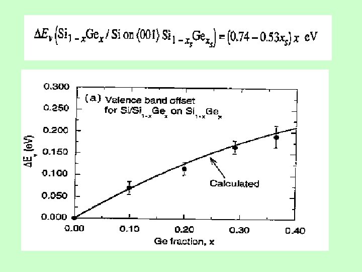
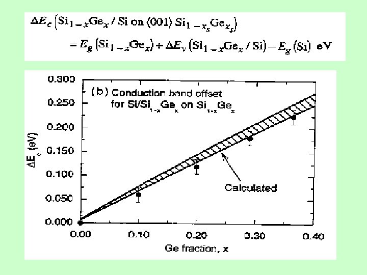
 as a function of Ge fraction x")


 and unstrained Si n-MOSFETs as a function of")


- Slides: 41
Strained Silicon MOSFET R 91943037 Jie-Ying Wei Department of Electrical Engineering and Graduate Institute of Electronics Engineering National Taiwan University, Taipei, Taiwan, R. O. C.
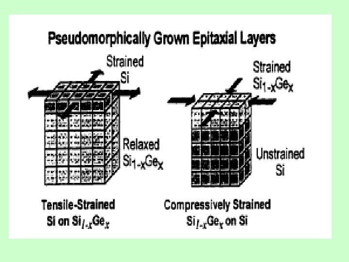
Cubic Lattice at Equilibrium
Lattice constant for a Si 1 -x. Gex alloy as a function of x
Critical thickness of Si 1 -x. Gex layers as a function of Ge fraction
The size change of each valley in a constant energy surface diagram indicates a shift up(smaller) or down(larger) in energy
LH:light hole band HH:heavy hole band SO:spin-orbit band
Sub-bands in an MOS inversion layer. Additional energy separation reduces inter-valley scattering
Band Alignment
Surface Channel MOSFET Structure
Extraction • Mobility • Band Offsets
Mobility
Split C-V measurement configuration
Measured split C-V capacitance from a surface strained-Si n-MOSFET grown on a relaxed-Si 0. 7 Ge 0. 3 VT : the intersection of the CGC and CGB curves
Gate-channel capacitance curve CGC
Gate-bulk capacitance curve CGB
When VGS < V FB , holes begin to accumulate at the Si/Si. Ge interface, confined by the valence band offset. The hole confinement causes the observed plateau at C’OX in CGB curve.
Effective mobility of surface-channel, strained-Si n-MOSFET at room temperature (Na=2 E 16)
Peak mobility enhancement ratio at room temperature as a function of apparent Ge fractions in the buffer layer
Transconductance for W*L = 5*10 µm strained-Si n-MOSFETs Performance saturation with Ge fractions x > 0. 2
Extraction • Mobility • Band Offsets
Full C-V characteristics of a surface strained-Si n-MOSFET (on relaxed Si 0. 7 Ge 0. 3) compared to a CZ Si control
Some parameters • Qf : match the flatband voltages between the measured data and theoretical curves • ΔEC = ΔVT since thickness of the Si channel(10 nm) is less than the Debye length of the material(20 nm) • ΔEV : the difference between Va and V’a is not straight-forward, so simulation of theoretical curve is required
Threshold voltage shift (ΔVT ) as a function of Ge fraction x
Two major assumptions in band offset extraction using SEDAN simulation • All material properties, other than the bandgap, in strained-Si and relaxed Si. Ge are identical to bulk Si. The results may be affected by 1. the material dielectric constant 2. the electron affinity 3. the density-of-state (DOS) effective mass • Data of Braunstein, at al. is accurate for the bandgap of relaxed Si. Ge.
The results were identical, except for a shift in the flatband voltage
Strained-Si band parameters and channel thickness extracted from C-V measurments
Bandgap of strained-Si grown on a relaxed Si. Ge buffer layer
IEDM 2002 1. Strained Silicon MOSFET Technology 2. Low Field Mobility Characteristics of Sub -100 nm Unstrained and Strained Si MOSFETs
Strained Silicon MOSFET Technology Schematic illustration a surface-channel strained-Si n-MOSFET
Effective mobility enhancement ratios
Mobility behavior in strained Si(20% Ge) and unstrained Si n-MOSFETs as a function of doping
Comparison of hole mobility enhancement ratios in strained Si p-MOSFETs as a function of vertical effective field, Eeff
Low field Mobility Characteristics of Sub 100 nm Unstrained and Strained Si MOSFETs
The slopes of the lines were used to calculate mobility
Comparison of mobility extracted on long channel and short channel devices using the conventional and d. R/d. L method
Mobility enhancement factor as a function of temperature
Reference 1. Jeffrey John Welser “ The application of strainedsilicon/relaxed-silicon germanium heterostructures to metal-oxide-semiconductor field-effect transistors” 2. Kern Rim “Application of silicon-based heterostructures to enhanced mobility metal-oxidesemiconductor field-effect transistors” 3. J. L. Hoyt, IEDM 2002 4. K. Rim, IEDM 2002