Outline Thesis organization Chapter 2Straininduced Raman Shift Chapter
- Slides: 43


Outline □ □ □ □ Thesis organization Chapter 2:Strain-induced Raman Shift Chapter 3:Carrier Mobility in Orthorhombically Strained Silicon Chapter 4: 2 -D Electrons in Strained Silicon Inversion Layers Chapter 5:Surface Effect on Strained Silicon Clusters Chapter 6:Strain Effect on Silicon Atomic Wires Summary and Future Work NTU GIEE Nano. Si. OE 2

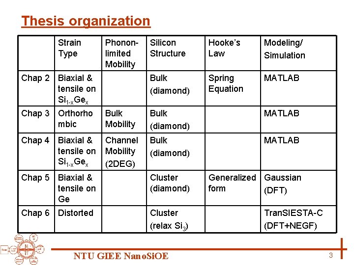
Thesis organization Strain Type Phononlimited Mobility Chap 2 Biaxial & tensile on Si 1 -x. Gex Silicon Structure Hooke’s Law Modeling/ Simulation Bulk (diamond) Spring Equation MATLAB Chap 3 Orthorho mbic Bulk Mobility Bulk (diamond) MATLAB Chap 4 Biaxial & tensile on Si 1 -x. Gex Channel Mobility (2 DEG) Bulk (diamond) MATLAB Chap 5 Biaxial & tensile on Ge Cluster (diamond) Generalized Gaussian form (DFT) Chap 6 Distorted Cluster (relax Si 3) NTU GIEE Nano. Si. OE Tran. SIESTA-C (DFT+NEGF) 3

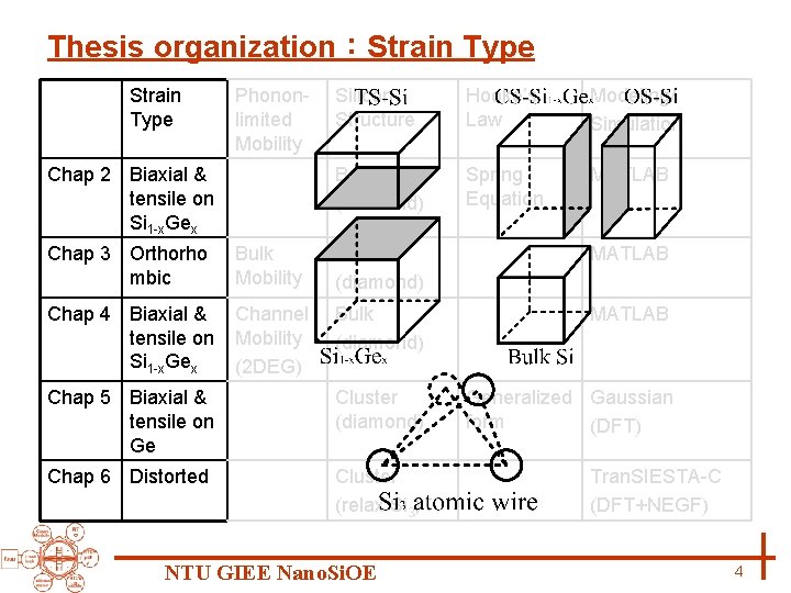
Thesis organization:Strain Type Phononlimited Mobility Chap 2 Biaxial & tensile on Si 1 -x. Gex Silicon Structure Hooke’s Law Modeling/ Simulation Bulk (diamond) Spring Equation MATLAB Chap 3 Orthorho mbic Bulk Mobility Bulk (diamond) MATLAB Chap 4 Biaxial & tensile on Si 1 -x. Gex Channel Mobility (2 DEG) Bulk (diamond) MATLAB Chap 5 Biaxial & tensile on Ge Cluster (diamond) Generalized Gaussian form (DFT) Chap 6 Distorted Cluster (relax Si 3) NTU GIEE Nano. Si. OE Tran. SIESTA-C (DFT+NEGF) 4

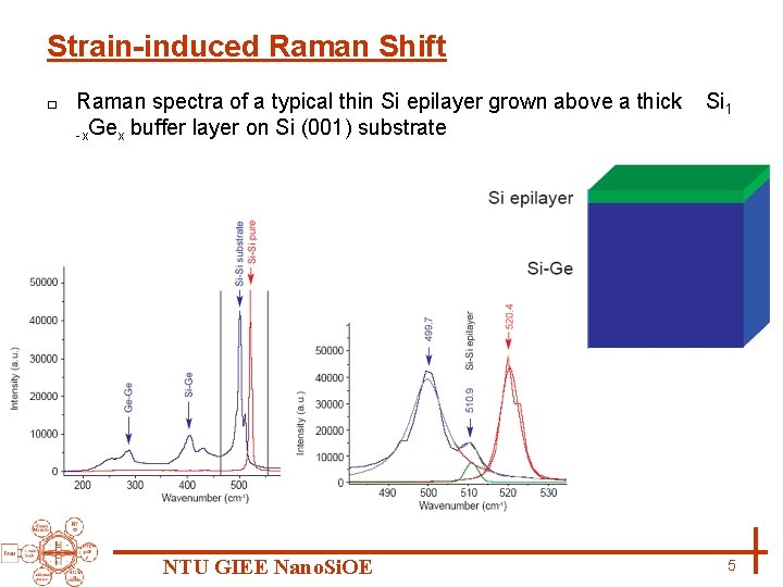
Strain-induced Raman Shift □ Raman spectra of a typical thin Si epilayer grown above a thick -x. Gex buffer layer on Si (001) substrate NTU GIEE Nano. Si. OE Si 1 5

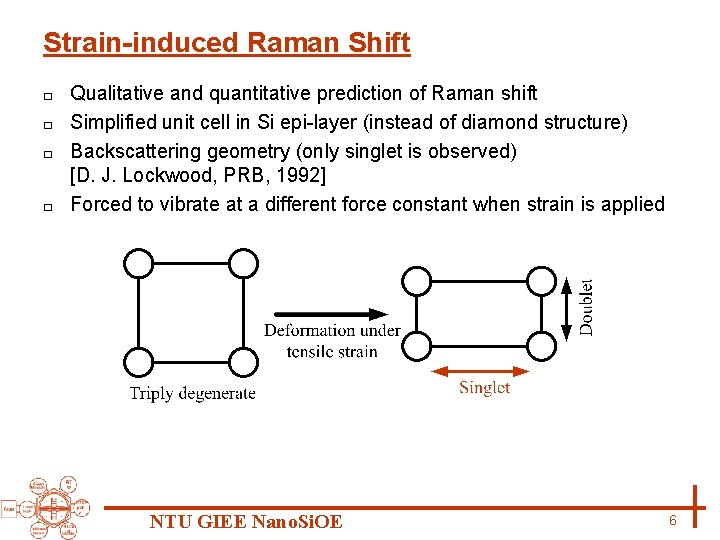
Strain-induced Raman Shift Qualitative and quantitative prediction of Raman shift □ Simplified unit cell in Si epi-layer (instead of diamond structure) □ Backscattering geometry (only singlet is observed) [D. J. Lockwood, PRB, 1992] □ Forced to vibrate at a different force constant when strain is applied □ NTU GIEE Nano. Si. OE 6

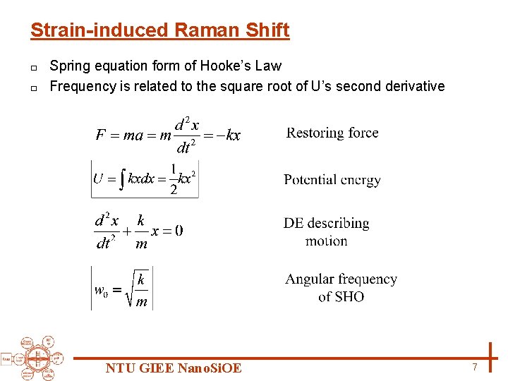
Strain-induced Raman Shift Spring equation form of Hooke’s Law □ Frequency is related to the square root of U’s second derivative □ NTU GIEE Nano. Si. OE 7

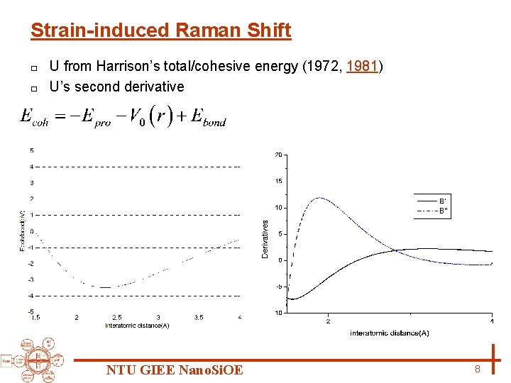
Strain-induced Raman Shift U from Harrison’s total/cohesive energy (1972, 1981) □ U’s second derivative □ NTU GIEE Nano. Si. OE 8

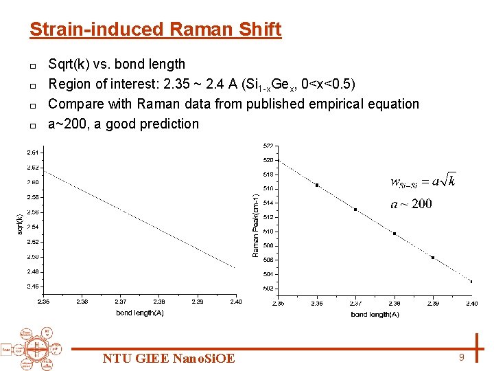
Strain-induced Raman Shift Sqrt(k) vs. bond length □ Region of interest: 2. 35 ~ 2. 4 A (Si 1 -x. Gex, 0<x<0. 5) □ Compare with Raman data from published empirical equation □ a~200, a good prediction □ NTU GIEE Nano. Si. OE 9

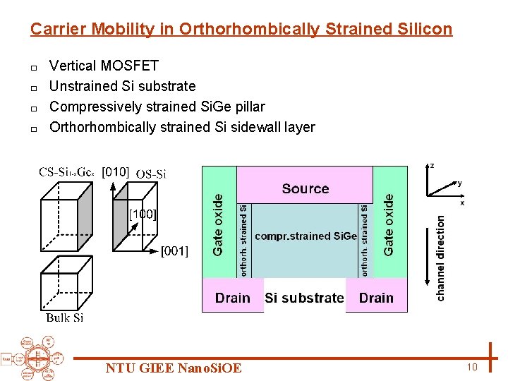
Carrier Mobility in Orthorhombically Strained Silicon Vertical MOSFET □ Unstrained Si substrate □ Compressively strained Si. Ge pillar □ Orthorhombically strained Si sidewall layer □ NTU GIEE Nano. Si. OE 10

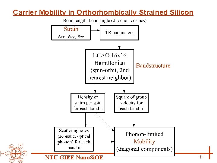
Carrier Mobility in Orthorhombically Strained Silicon NTU GIEE Nano. Si. OE 11

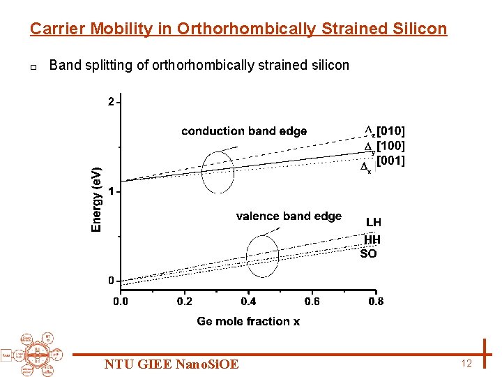
Carrier Mobility in Orthorhombically Strained Silicon □ Band splitting of orthorhombically strained silicon NTU GIEE Nano. Si. OE 12

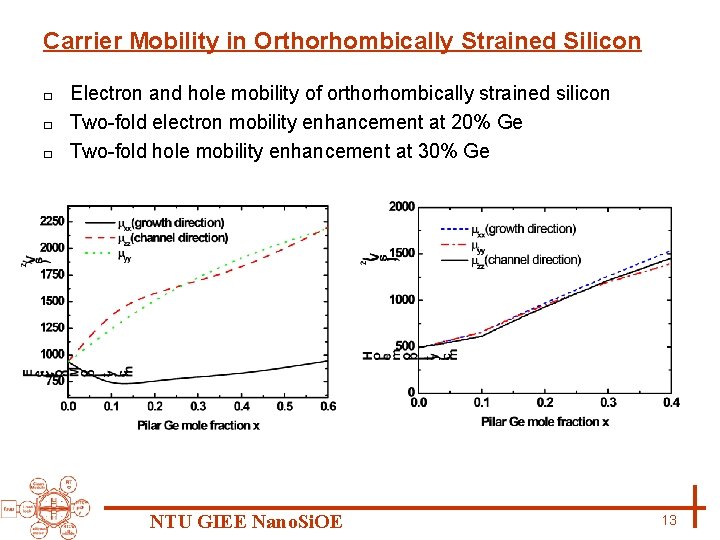
Carrier Mobility in Orthorhombically Strained Silicon Electron and hole mobility of orthorhombically strained silicon □ Two-fold electron mobility enhancement at 20% Ge □ Two-fold hole mobility enhancement at 30% Ge □ NTU GIEE Nano. Si. OE 13

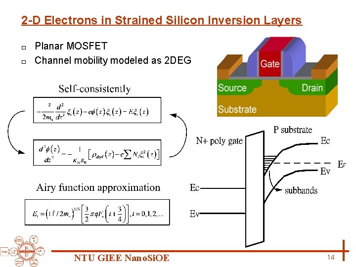
2 -D Electrons in Strained Silicon Inversion Layers Planar MOSFET □ Channel mobility modeled as 2 DEG □ NTU GIEE Nano. Si. OE 14

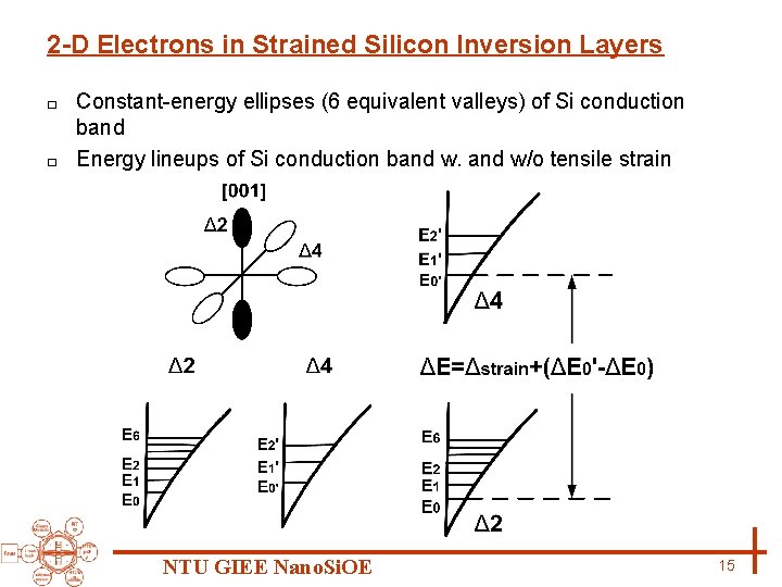
2 -D Electrons in Strained Silicon Inversion Layers Constant-energy ellipses (6 equivalent valleys) of Si conduction band □ Energy lineups of Si conduction band w/o tensile strain □ NTU GIEE Nano. Si. OE 15

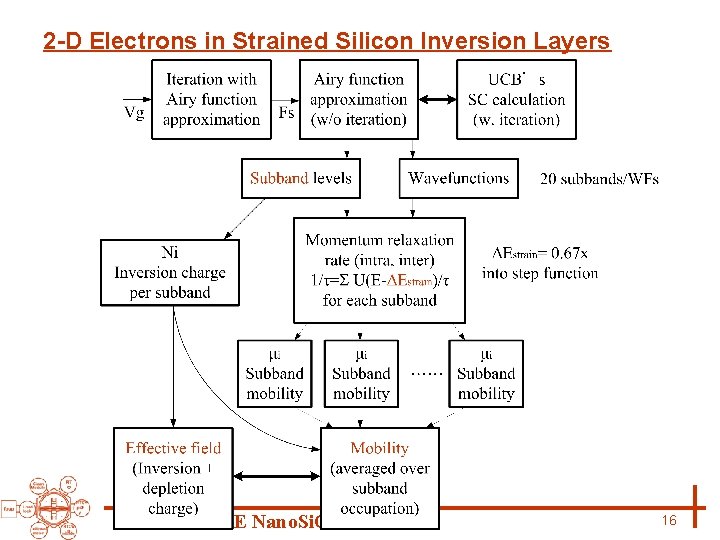
2 -D Electrons in Strained Silicon Inversion Layers NTU GIEE Nano. Si. OE 16

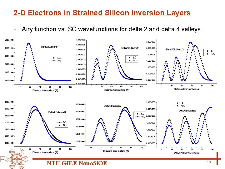
2 -D Electrons in Strained Silicon Inversion Layers □ Airy function vs. SC wavefunctions for delta 2 and delta 4 valleys NTU GIEE Nano. Si. OE 17

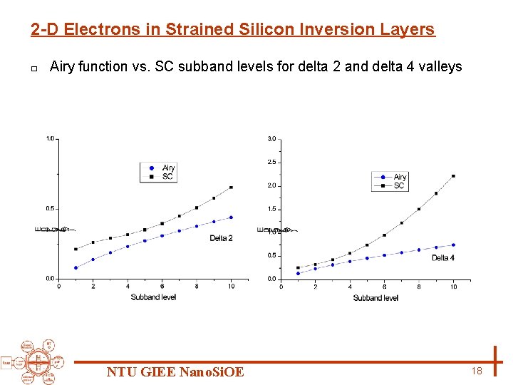
2 -D Electrons in Strained Silicon Inversion Layers □ Airy function vs. SC subband levels for delta 2 and delta 4 valleys NTU GIEE Nano. Si. OE 18

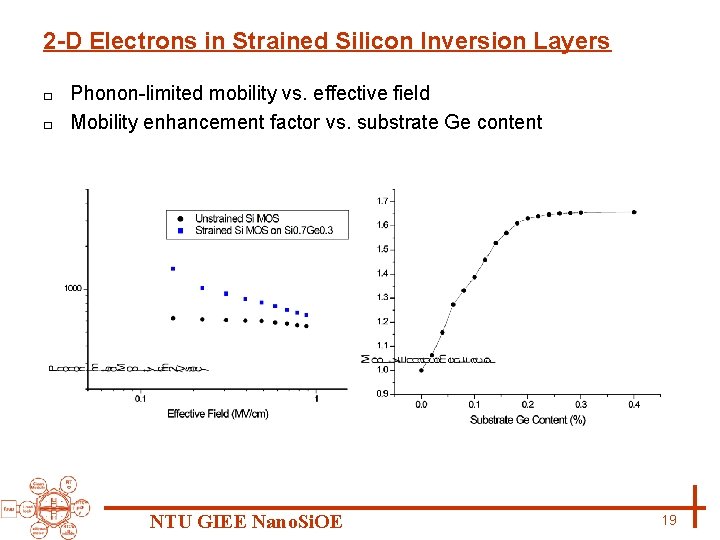
2 -D Electrons in Strained Silicon Inversion Layers Phonon-limited mobility vs. effective field □ Mobility enhancement factor vs. substrate Ge content □ NTU GIEE Nano. Si. OE 19

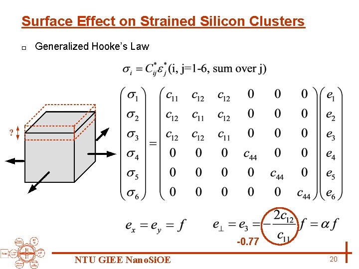
Surface Effect on Strained Silicon Clusters □ Generalized Hooke’s Law -0. 77 NTU GIEE Nano. Si. OE 20

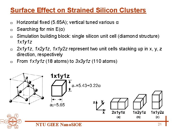
Surface Effect on Strained Silicon Clusters □ □ □ Horizontal fixed (5. 65 A); vertical tuned various α Searching for min E(α) Simulation building block: single silicon unit cell (diamond structure) 1 x 1 y 1 z 2 x 1 y 1 z, 1 x 2 y 1 z, 1 x 1 y 2 z represent two unit cells stacking up in x, y, z direction, respectively From 1 x 1 y 1 z (18 atoms) to 3 x 3 y 1 z (110 atoms) NTU GIEE Nano. Si. OE 21

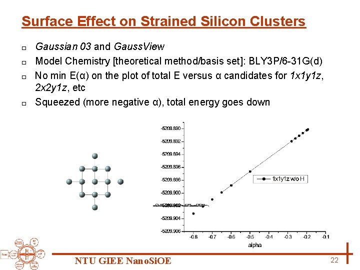
Surface Effect on Strained Silicon Clusters Gaussian 03 and Gauss. View □ Model Chemistry [theoretical method/basis set]: BLY 3 P/6 -31 G(d) □ No min E(α) on the plot of total E versus α candidates for 1 x 1 y 1 z, 2 x 2 y 1 z, etc □ Squeezed (more negative α), total energy goes down □ NTU GIEE Nano. Si. OE 22

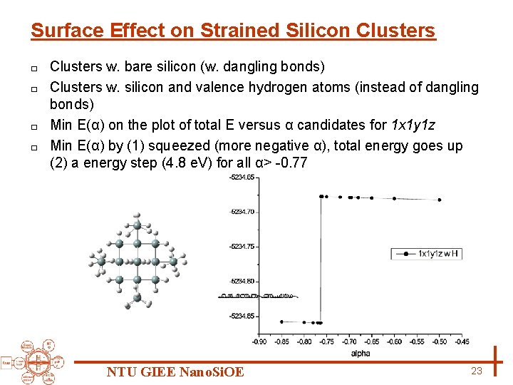
Surface Effect on Strained Silicon Clusters w. bare silicon (w. dangling bonds) □ Clusters w. silicon and valence hydrogen atoms (instead of dangling bonds) □ Min E(α) on the plot of total E versus α candidates for 1 x 1 y 1 z □ Min E(α) by (1) squeezed (more negative α), total energy goes up (2) a energy step (4. 8 e. V) for all α> -0. 77 □ NTU GIEE Nano. Si. OE 23

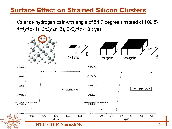
Surface Effect on Strained Silicon Clusters Valence hydrogen pair with angle of 54. 7 degree (instead of 109. 8) □ 1 x 1 y 1 z (1), 2 x 2 y 1 z (5), 3 x 3 y 1 z (13): yes □ NTU GIEE Nano. Si. OE 24

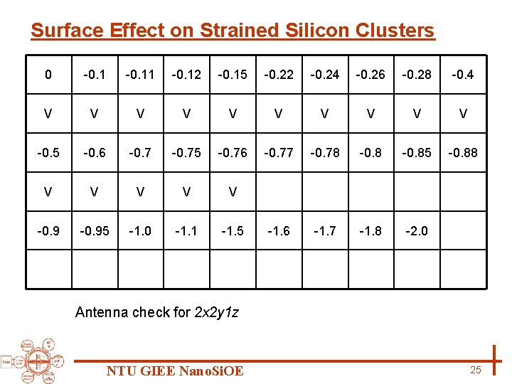
Surface Effect on Strained Silicon Clusters 0 -0. 11 -0. 12 -0. 15 -0. 22 -0. 24 -0. 26 -0. 28 -0. 4 V V V V V -0. 5 -0. 6 -0. 75 -0. 76 -0. 77 -0. 78 -0. 85 -0. 88 V V V -0. 95 -1. 0 -1. 1 -1. 5 -1. 6 -1. 7 -1. 8 -2. 0 Antenna check for 2 x 2 y 1 z NTU GIEE Nano. Si. OE 25

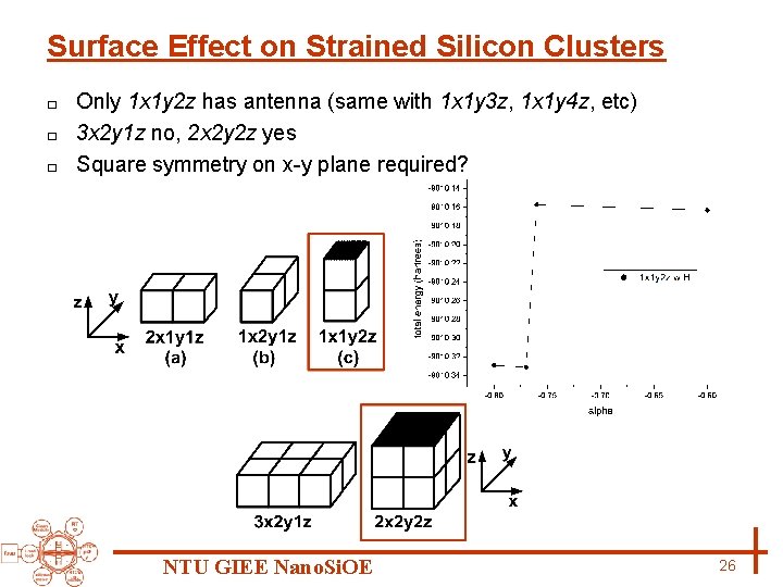
Surface Effect on Strained Silicon Clusters Only 1 x 1 y 2 z has antenna (same with 1 x 1 y 3 z, 1 x 1 y 4 z, etc) □ 3 x 2 y 1 z no, 2 x 2 y 2 z yes □ Square symmetry on x-y plane required? □ NTU GIEE Nano. Si. OE 26

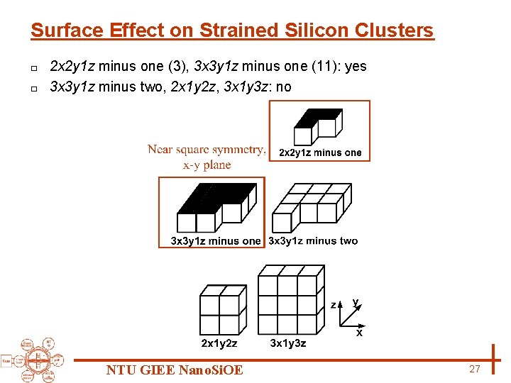
Surface Effect on Strained Silicon Clusters 2 x 2 y 1 z minus one (3), 3 x 3 y 1 z minus one (11): yes □ 3 x 3 y 1 z minus two, 2 x 1 y 2 z, 3 x 1 y 3 z: no □ NTU GIEE Nano. Si. OE 27

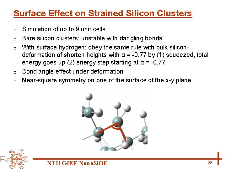
Surface Effect on Strained Silicon Clusters □ □ □ Simulation of up to 9 unit cells Bare silicon clusters: unstable with dangling bonds With surface hydrogen: obey the same rule with bulk silicondeformation of shorten heights with α = -0. 77 by (1) squeezed, total energy goes up (2) energy step starting at α = -0. 77 Bond angle effect under deformation Near-square symmetry on one of the surface of the x-y plane NTU GIEE Nano. Si. OE 28

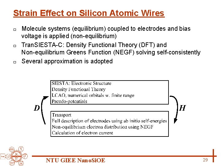
Strain Effect on Silicon Atomic Wires Molecule systems (equilibrium) coupled to electrodes and bias voltage is applied (non-equilibrium) □ Tran. SIESTA-C: Density Functional Theory (DFT) and Non-equilibrium Greens Function (NEGF) solving self-consistently □ Several approximation is adopted □ NTU GIEE Nano. Si. OE 29

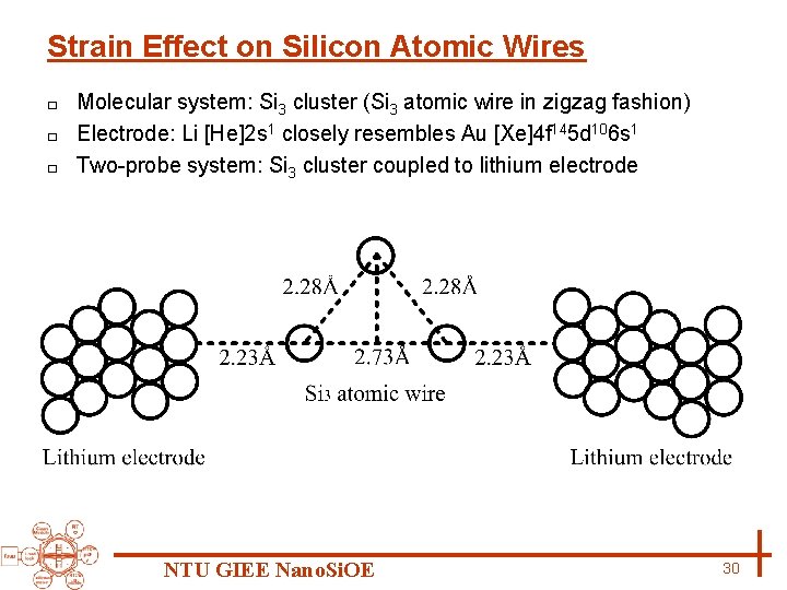
Strain Effect on Silicon Atomic Wires Molecular system: Si 3 cluster (Si 3 atomic wire in zigzag fashion) □ Electrode: Li [He]2 s 1 closely resembles Au [Xe]4 f 145 d 106 s 1 □ Two-probe system: Si 3 cluster coupled to lithium electrode □ NTU GIEE Nano. Si. OE 30

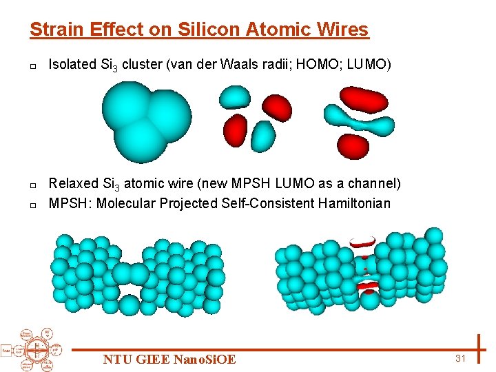
Strain Effect on Silicon Atomic Wires □ Isolated Si 3 cluster (van der Waals radii; HOMO; LUMO) Relaxed Si 3 atomic wire (new MPSH LUMO as a channel) □ MPSH: Molecular Projected Self-Consistent Hamiltonian □ NTU GIEE Nano. Si. OE 31

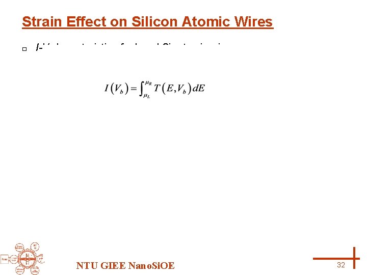
Strain Effect on Silicon Atomic Wires □ I-V characteristic of relaxed Si 3 atomic wire NTU GIEE Nano. Si. OE 32

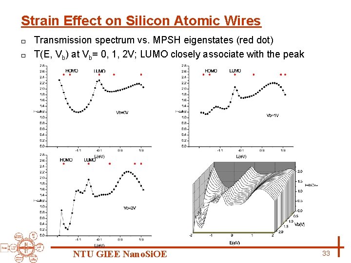
Strain Effect on Silicon Atomic Wires Transmission spectrum vs. MPSH eigenstates (red dot) □ T(E, Vb) at Vb= 0, 1, 2 V; LUMO closely associate with the peak □ NTU GIEE Nano. Si. OE 33

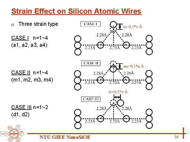
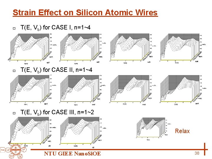
Strain Effect on Silicon Atomic Wires □ Three strain type CASE I n=1~4 (a 1, a 2, a 3, a 4) CASE II n=1~4 (m 1, m 2, m 3, m 4) CASE III n=1~2 (d 1, d 2) NTU GIEE Nano. Si. OE 34

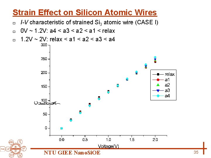
Strain Effect on Silicon Atomic Wires I-V characteristic of strained Si 3 atomic wire (CASE I) □ 0 V ~ 1. 2 V: a 4 < a 3 < a 2 < a 1 < relax □ 1. 2 V ~ 2 V: relax < a 1 < a 2 < a 3 < a 4 □ NTU GIEE Nano. Si. OE 35

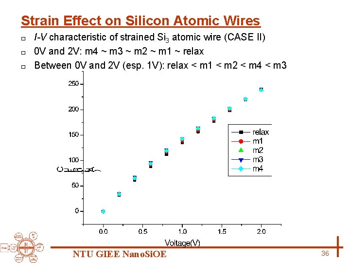
Strain Effect on Silicon Atomic Wires I-V characteristic of strained Si 3 atomic wire (CASE II) □ 0 V and 2 V: m 4 ~ m 3 ~ m 2 ~ m 1 ~ relax □ Between 0 V and 2 V (esp. 1 V): relax < m 1 < m 2 < m 4 < m 3 □ NTU GIEE Nano. Si. OE 36

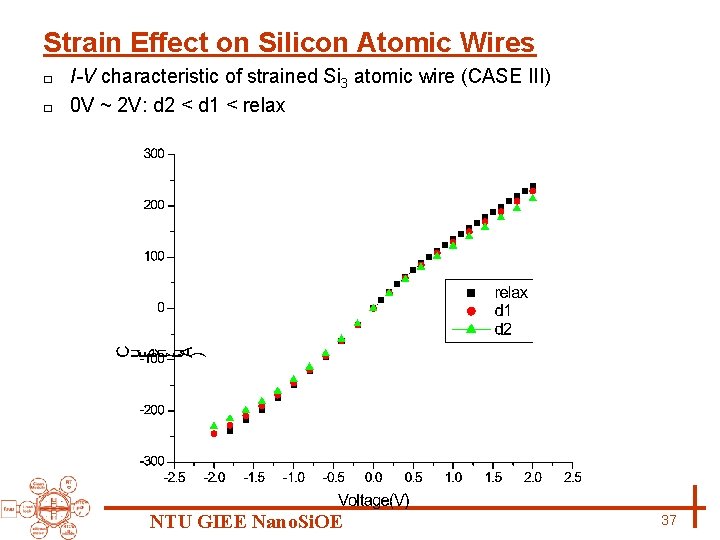
Strain Effect on Silicon Atomic Wires I-V characteristic of strained Si 3 atomic wire (CASE III) □ 0 V ~ 2 V: d 2 < d 1 < relax □ NTU GIEE Nano. Si. OE 37

Strain Effect on Silicon Atomic Wires □ T(E, Vb) for CASE I, n=1~4 □ T(E, Vb) for CASE III, n=1~2 Relax NTU GIEE Nano. Si. OE 38

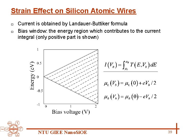
Strain Effect on Silicon Atomic Wires Current is obtained by Landauer-Buttiker formula □ Bias window: the energy region which contributes to the current integral (only positive part is shown) □ NTU GIEE Nano. Si. OE 39

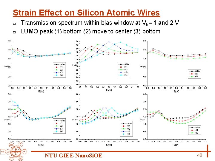
Strain Effect on Silicon Atomic Wires Transmission spectrum within bias window at Vb= 1 and 2 V □ LUMO peak (1) bottom (2) move to center (3) bottom □ NTU GIEE Nano. Si. OE 40

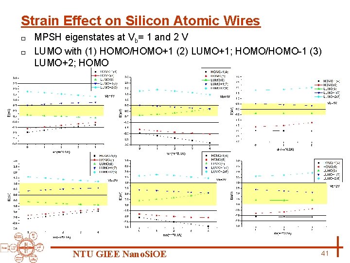
Strain Effect on Silicon Atomic Wires MPSH eigenstates at Vb= 1 and 2 V □ LUMO with (1) HOMO/HOMO+1 (2) LUMO+1; HOMO/HOMO-1 (3) LUMO+2; HOMO □ NTU GIEE Nano. Si. OE 41

Summary and Future Work:Summary □ □ □ A simple spring model is developed to make qualitative and quantitative predictions of Raman peak red-shift in tensile strain silicon epi-layer. Phonon-limited bulk mobility under orthorhombic strain is calculated. Strong electron and hole mobility enhancement is observed. Phonon-limited electron channel mobility under tensile strain is calculated. Airy function is a fair approximation. Enhancement factor saturates at 20% Ge content. Surface hydrogen atoms is necessary to stabilize silicon clusters up to 9 unit cells in a morphology of shorten heights (α = -0. 77) under tensile strain. Near square symmetry is required for above observation. I-V characteristic of relaxed and strained Si 3 atomic wire is investigated. Bias window and MPSH eigenstates are helpful in understanding the changes in I-V characteristic in three strain conditions. NTU GIEE Nano. Si. OE 42

Summary and Future Work:Future Work Experimental confirmation □ More sophisticated molecular electronics with realistic metal electrodes □ NTU GIEE Nano. Si. OE 43