Strained Silicon Aaron Prager EE 666 April 21









- Slides: 23

Strained Silicon Aaron Prager EE 666 April 21, 2005

Outline Introduction n CMOS Strained Silicon n Why is it good? How does it work? How do we make it? Conclusions

CMOS Complimentary Metal-Oxide-Semiconductor Basis for most computer chips We’re good at making CMOS!

Moore’s Law… More and more transistors every year Higher and higher speeds CMOS can’t get much smaller How can we continue innovating and moving faster?

Strained Silicon As gate length shrinks, mobility decreases n Increased doping to combat short channel effects Method to increase mobility of electrons and holes in the channel of an FET Tensile and compressive strain applied to channel

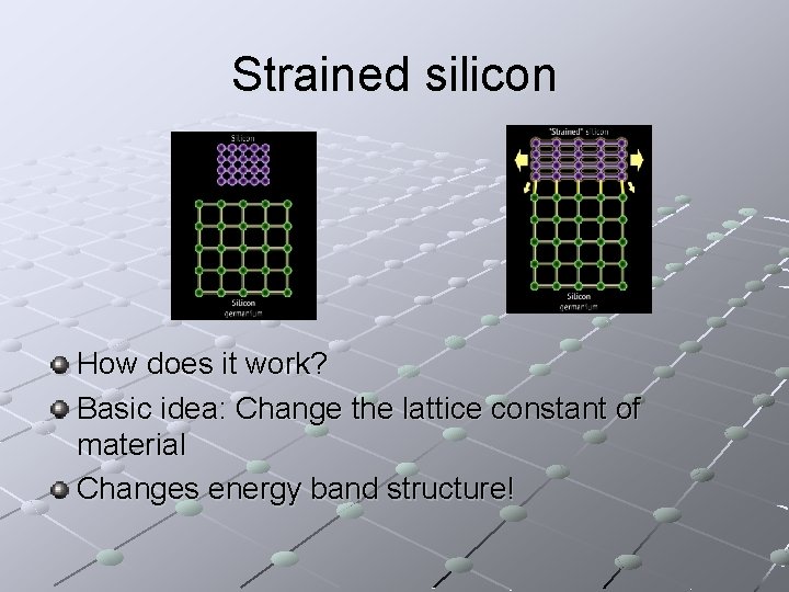
Strained silicon How does it work? Basic idea: Change the lattice constant of material Changes energy band structure!

Strained Silicon So, what is actually happening?

Strained Silicon: Electrons So, what is actually happening? Electrical symmetry destroyed by strain n Four energy valleys go down in energy, two go up (in biaxal strain) Vice versa in unaxial INTERVALLY SCATTERING REDUCED! Change in curvature n Reduction in effective mass! n

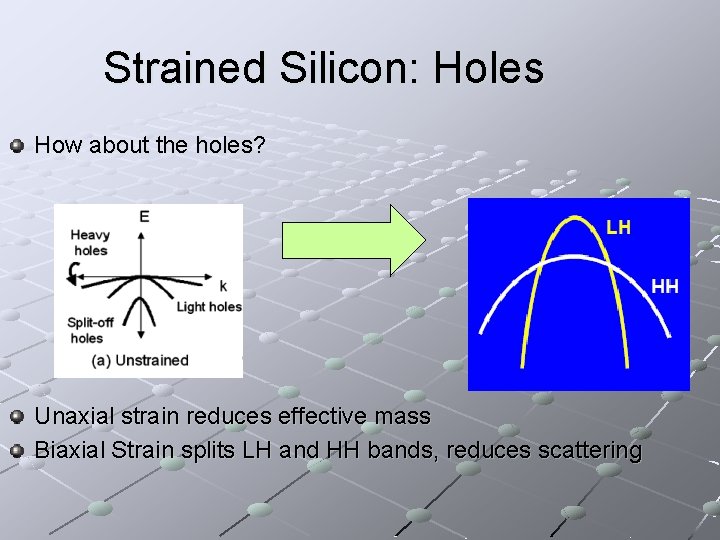
Strained Silicon: Holes How about the holes? Unaxial strain reduces effective mass Biaxial Strain splits LH and HH bands, reduces scattering

Fabrication Effect was noticed in early 1950’s n n Generally an effect to be avoided Why bother? In recent years scaling has become more difficult Idea revived at MIT in early 1990 s

Fabrication Two types of strain n n Compressive Tensile Two “directions” of strain n n Unaxial Biaxial

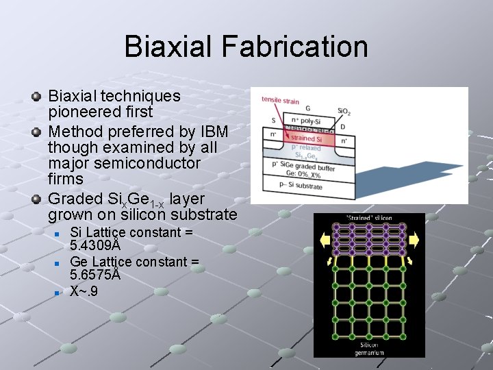
Biaxial Fabrication Biaxial techniques pioneered first Method preferred by IBM though examined by all major semiconductor firms Graded Six. Ge 1 -x layer grown on silicon substrate n n n Si Lattice constant = 5. 4309Å Ge Lattice constant = 5. 6575Å X~. 9

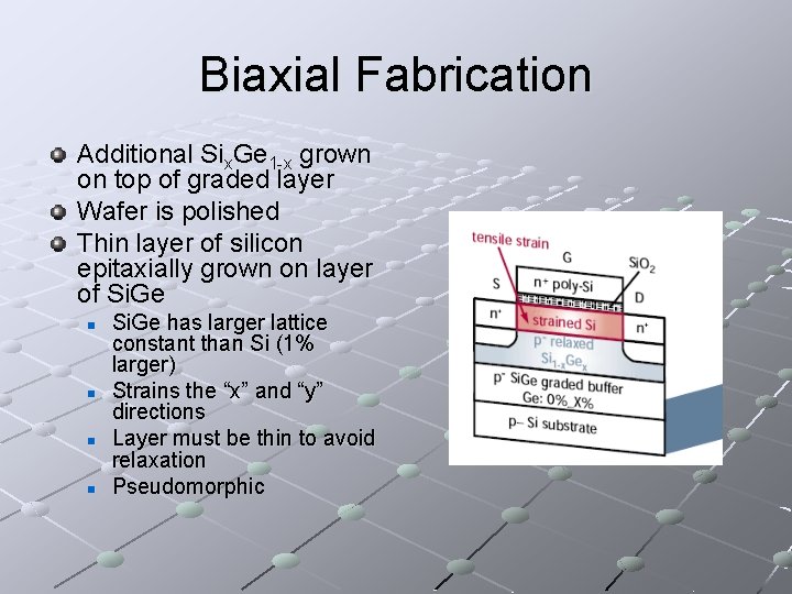
Biaxial Fabrication Additional Six. Ge 1 -x grown on top of graded layer Wafer is polished Thin layer of silicon epitaxially grown on layer of Si. Ge n n Si. Ge has larger lattice constant than Si (1% larger) Strains the “x” and “y” directions Layer must be thin to avoid relaxation Pseudomorphic

Biaxial Fabrication Increases electron mobility No great change in hole mobility Has problems n n n Diffusion of Ge into Si Dislocations Cost (? )

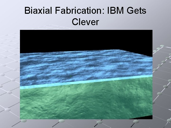
Biaxial Fabrication: IBM Gets Clever First cleverness: Si. Ge on insulator, with silicon epitaxially grown on Si. Ge n Positive benefits of SOI (lower capacitances, faster switching, lower leakage) as well as benefits of strain But wouldn’t it be good if we could do strained silicon on insulator without Si. Ge underlayer?

Biaxial Fabrication: IBM Gets Clever

Biaxial Strain IBM proposing strained Germanium channel n n n Excellent electrical properties Hard to grow insulator Epitaxial growth makes it possible

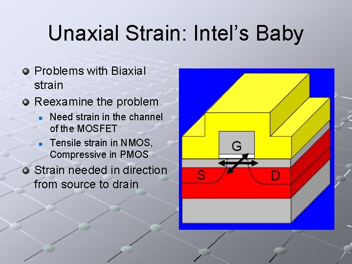
Unaxial Strain: Intel’s Baby Problems with Biaxial strain Reexamine the problem n n Need strain in the channel of the MOSFET Tensile strain in NMOS, Compressive in PMOS Strain needed in direction from source to drain

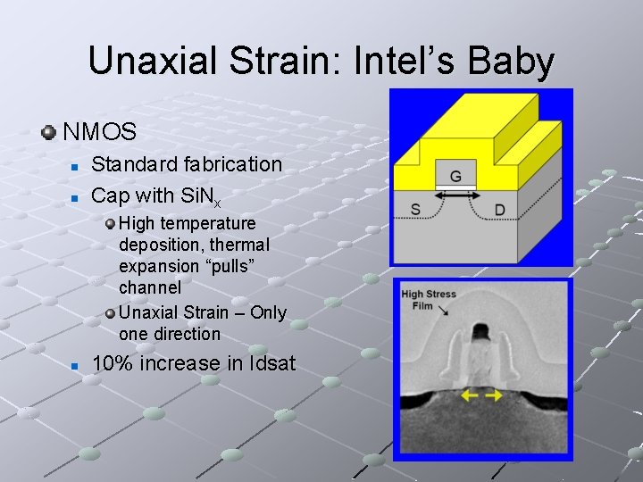
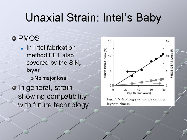
Unaxial Strain: Intel’s Baby NMOS n n Standard fabrication Cap with Si. Nx High temperature deposition, thermal expansion “pulls” channel Unaxial Strain – Only one direction n 10% increase in Idsat

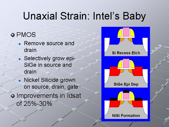
Unaxial Strain: Intel’s Baby PMOS n n n Remove source and drain Selectively grow epi. Si. Ge in source and drain Nickel Silicide grown on source, drain, gate Improvements in Idsat of 25%-30%

Unaxial Strain: Intel’s Baby PMOS n In Intel fabrication method FET also covered by the Si. Nx layer No major loss! In general, strain showing compatibility with future technology

Quantum Effects Strain always a problem n n Unwanted strain changes wave functions Work always done to remove strain Proposals to actually increase strain instead Remove all energy valleys except one, meaning no other changes could occur

Conclusions Strain in Silicon can increase mobility in NMOS and PMOS FETs Biaxial and Unaxial strain techniques developed In use by major players