PGT 315 RF AND MICROWAVE TECHNOLOGY CHAPTER 2
![Cont’d… • From equation [2. 1], c = 3 x 10⁸ m/sec is the Cont’d… • From equation [2. 1], c = 3 x 10⁸ m/sec is the](https://slidetodoc.com/presentation_image_h/2fcaaf6ab59714b42bb6c889ce84ecbe/image-11.jpg)
![Cont’d… • With: [2. 10] [2. 11] Where t is the thickness of the Cont’d… • With: [2. 10] [2. 11] Where t is the thickness of the](https://slidetodoc.com/presentation_image_h/2fcaaf6ab59714b42bb6c889ce84ecbe/image-15.jpg)
![Cont’d… • The capacitance per unit length of the stripline is: [2. 14] • Cont’d… • The capacitance per unit length of the stripline is: [2. 14] •](https://slidetodoc.com/presentation_image_h/2fcaaf6ab59714b42bb6c889ce84ecbe/image-20.jpg)
![Cont’d… The phase velocity and the propagation constant: [2. 16] [2. 17] Where εe Cont’d… The phase velocity and the propagation constant: [2. 16] [2. 17] Where εe](https://slidetodoc.com/presentation_image_h/2fcaaf6ab59714b42bb6c889ce84ecbe/image-24.jpg)
![Cont’d… The effective dielectric constant of a microstrip line is given by: [2. 18] Cont’d… The effective dielectric constant of a microstrip line is given by: [2. 18]](https://slidetodoc.com/presentation_image_h/2fcaaf6ab59714b42bb6c889ce84ecbe/image-25.jpg)
![Cont’d… The characteristic impedance can be calculated as: [2. 19] For a given characteristic Cont’d… The characteristic impedance can be calculated as: [2. 19] For a given characteristic](https://slidetodoc.com/presentation_image_h/2fcaaf6ab59714b42bb6c889ce84ecbe/image-26.jpg)

- Slides: 38

PGT 315 RF AND MICROWAVE TECHNOLOGY CHAPTER 2: PLANAR TRANSMISSION LINE 1

Transmission Lines • A device used to transfer energy from one point to another point “efficiently”. • Efficiently = minimum loss, reflection and close to a perfect match as possible (VSWR = 1: 1). • Important to be efficient at RF and microwave frequencies, since frequency used are higher than DC and low frequency applications. • As frequency gets higher, any energy loss is in transmission lines are more difficult and costly to be retrieved. 2

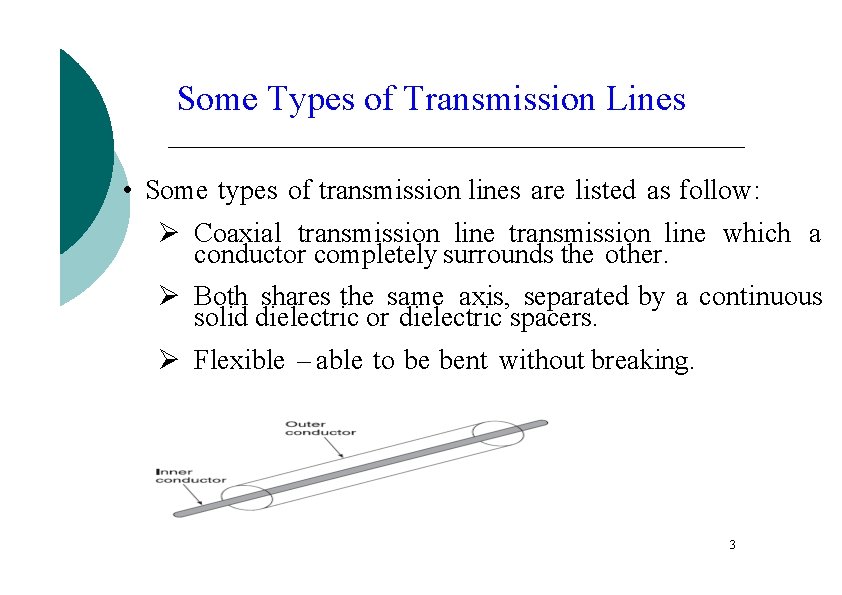
Some Types of Transmission Lines • Some types of transmission lines are listed as follow: Ø Coaxial transmission line which a conductor completely surrounds the other. Ø Both shares the same axis, separated by a continuous solid dielectric or dielectric spacers. Ø Flexible – able to be bent without breaking. 3

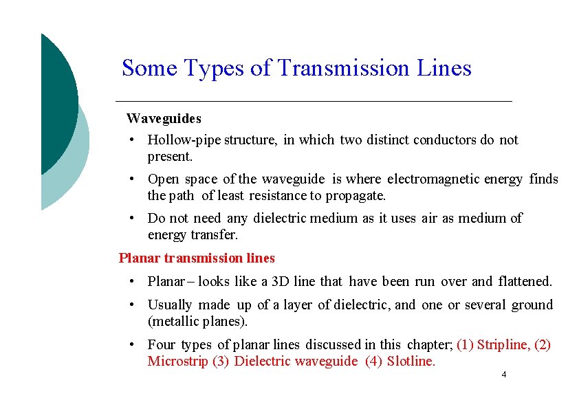
Some Types of Transmission Lines Waveguides • Hollow-pipe structure, in which two distinct conductors do not present. • Open space of the waveguide is where electromagnetic energy finds the path of least resistance to propagate. • Do not need any dielectric medium as it uses air as medium of energy transfer. Planar transmission lines • Planar – looks like a 3 D line that have been run over and flattened. • Usually made up of a layer of dielectric, and one or several ground (metallic planes). • Four types of planar lines discussed in this chapter; (1) Stripline, (2) Microstrip (3) Dielectric waveguide (4) Slotline. 4

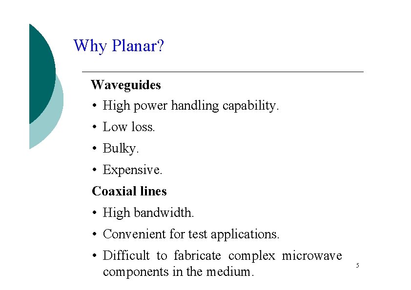
Why Planar? Waveguides • High power handling capability. • Low loss. • Bulky. • Expensive. Coaxial lines • High bandwidth. • Convenient for test applications. • Difficult to fabricate complex microwave components in the medium. 5

Cont’d… Planar Transmission Lines • Compact. • Low cost. • Capability for integration with active devices, such as diodes, transistors, etc. 6

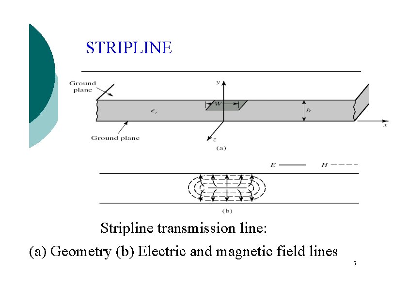
STRIPLINE Stripline transmission line: (a) Geometry (b) Electric and magnetic field lines 7

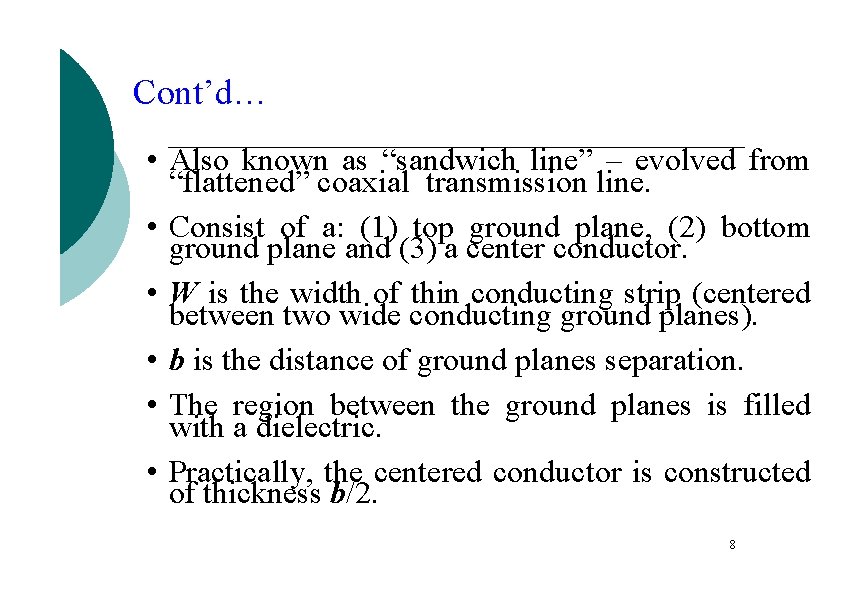
Cont’d… • Also known as “sandwich line” – evolved from “flattened” coaxial transmission line. • Consist of a: (1) top ground plane, (2) bottom ground plane and (3) a center conductor. • W is the width of thin conducting strip (centered between two wide conducting ground planes). • b is the distance of ground planes separation. • The region between the ground planes is filled with a dielectric. • Practically, the centered conductor is constructed of thickness b/2. 8

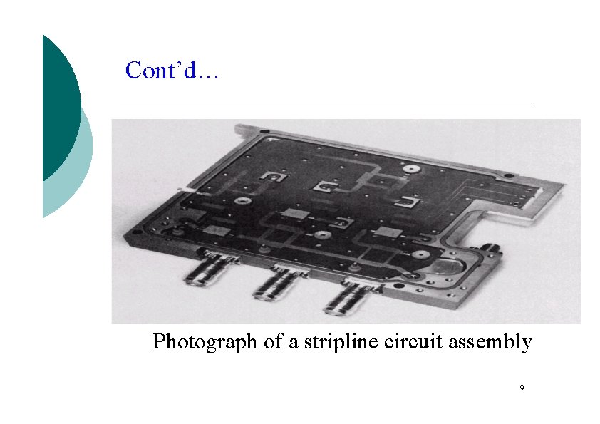
Cont’d… Photograph of a stripline circuit assembly 9

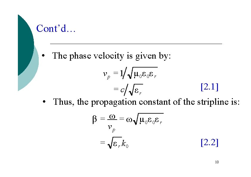
Cont’d… • The phase velocity is given by: vp = 1 µ 0ε 0ε r [2. 1] = c εr • Thus, the propagation constant of the stripline is: β = ω µ 0ε 0ε r vp = ε r k 0 [2. 2] 10
![Contd From equation 2 1 c 3 x 10⁸ msec is the Cont’d… • From equation [2. 1], c = 3 x 10⁸ m/sec is the](https://slidetodoc.com/presentation_image_h/2fcaaf6ab59714b42bb6c889ce84ecbe/image-11.jpg)
Cont’d… • From equation [2. 1], c = 3 x 10⁸ m/sec is the speed of light in free-space. • The characteristic impedance of a transmission line is given by: L LC 1 [2. 3] = = Z 0 = C C v p. C • L and C are the inductance and capacitance per unit length of the line. • The resulting formula for the characteristic impedance is: 30π b Z 0 = ε r We + 0. 441 b [2. 4] 11

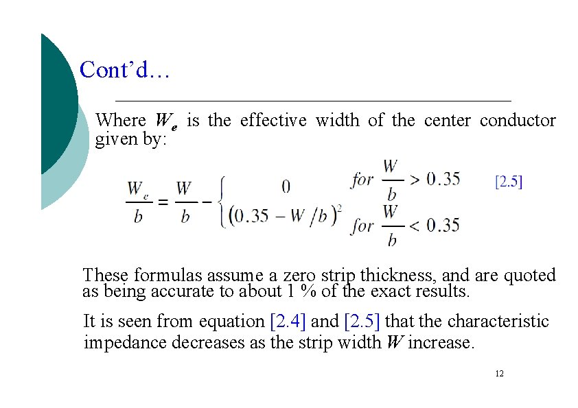
Cont’d… Where We is the effective width of the center conductor given by: These formulas assume a zero strip thickness, and are quoted as being accurate to about 1 % of the exact results. It is seen from equation [2. 4] and [2. 5] that the characteristic impedance decreases as the strip width W increase. 12

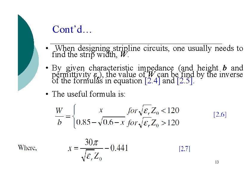
Cont’d… • When designing stripline circuits, one usually needs to find the strip width, W. • By given characteristic impedance (and height b and permittivity εr), the value of W can be find by the inverse of the formulas in equation [2. 4] and [2. 5]. • The useful formula is: 13

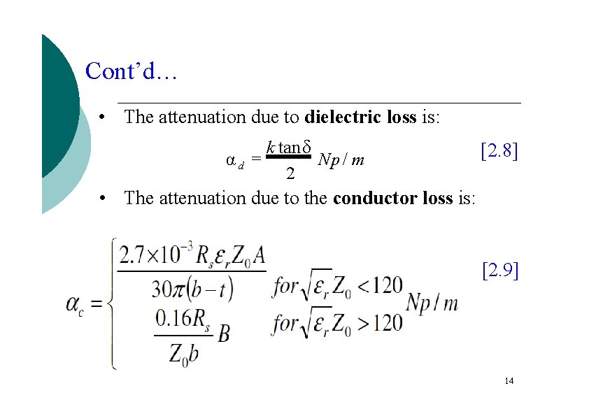
Cont’d… • The attenuation due to dielectric loss is: k tan δ Np / m αd = 2 [2. 8] • The attenuation due to the conductor loss is: [2. 9] 14
![Contd With 2 10 2 11 Where t is the thickness of the Cont’d… • With: [2. 10] [2. 11] Where t is the thickness of the](https://slidetodoc.com/presentation_image_h/2fcaaf6ab59714b42bb6c889ce84ecbe/image-15.jpg)
Cont’d… • With: [2. 10] [2. 11] Where t is the thickness of the strip. 15

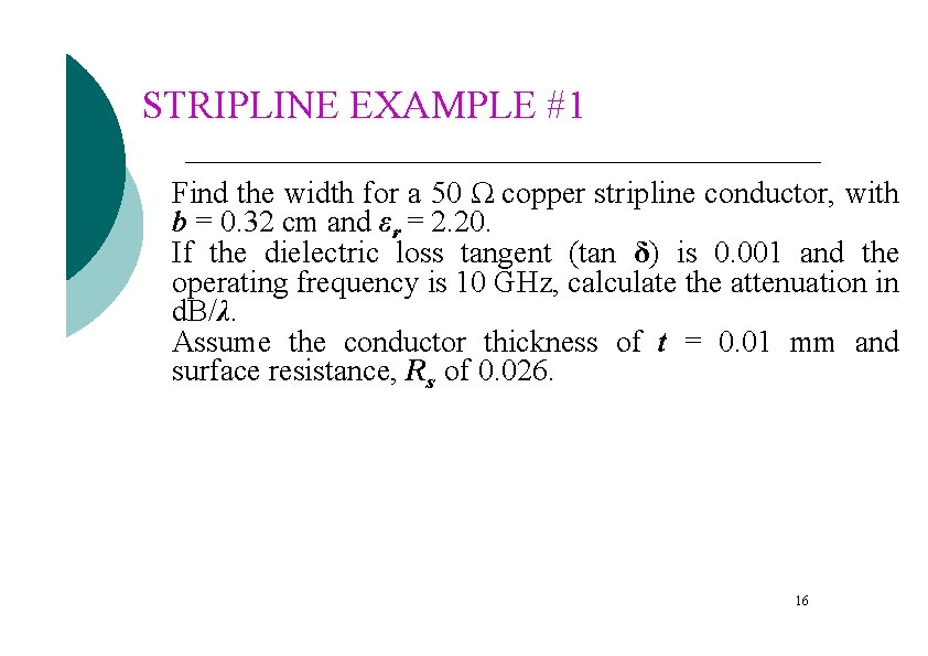
STRIPLINE EXAMPLE #1 Find the width for a 50 Ω copper stripline conductor, with b = 0. 32 cm and εr = 2. 20. If the dielectric loss tangent (tan δ) is 0. 001 and the operating frequency is 10 GHz, calculate the attenuation in d. B/λ. Assume the conductor thickness of t = 0. 01 mm and surface resistance, Rs of 0. 026. 16

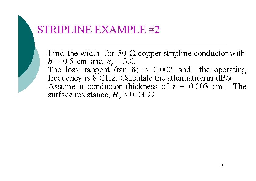
STRIPLINE EXAMPLE #2 Find the width for 50 Ω copper stripline conductor with b = 0. 5 cm and εr = 3. 0. The loss tangent (tan δ) is 0. 002 and the operating frequency is 8 GHz. Calculate the attenuation in d. B/λ. Assume a conductor thickness of t = 0. 003 cm. The surface resistance, Rs is 0. 03 Ω. 17

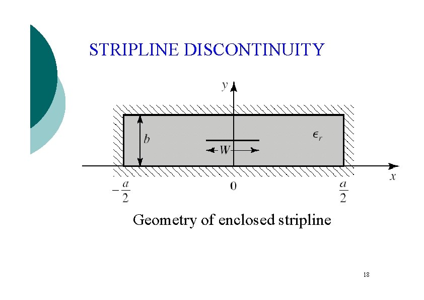
STRIPLINE DISCONTINUITY Geometry of enclosed stripline 18

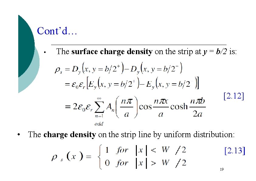
Cont’d… • The surface charge density on the strip at y = b/2 is: [2. 12] • The charge density on the strip line by uniform distribution: [2. 13] 19
![Contd The capacitance per unit length of the stripline is 2 14 Cont’d… • The capacitance per unit length of the stripline is: [2. 14] •](https://slidetodoc.com/presentation_image_h/2fcaaf6ab59714b42bb6c889ce84ecbe/image-20.jpg)
Cont’d… • The capacitance per unit length of the stripline is: [2. 14] • The characteristic impedance is then found as: [2. 15] 20

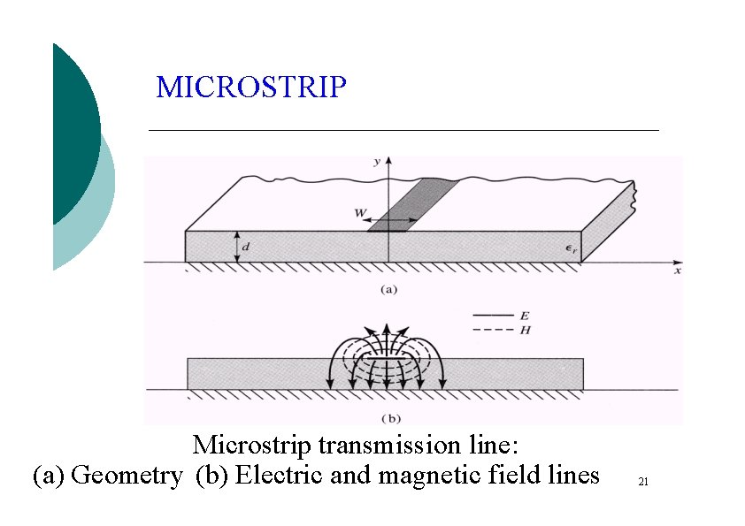
MICROSTRIP Microstrip transmission line: (a) Geometry (b) Electric and magnetic field lines 21

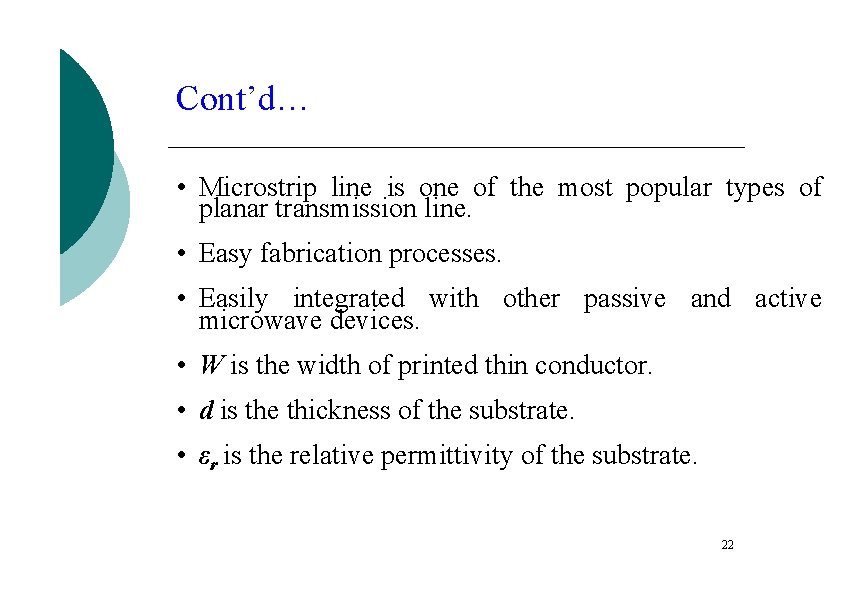
Cont’d… • Microstrip line is one of the most popular types of planar transmission line. • Easy fabrication processes. • Easily integrated with other passive and active microwave devices. • W is the width of printed thin conductor. • d is the thickness of the substrate. • εr is the relative permittivity of the substrate. 22

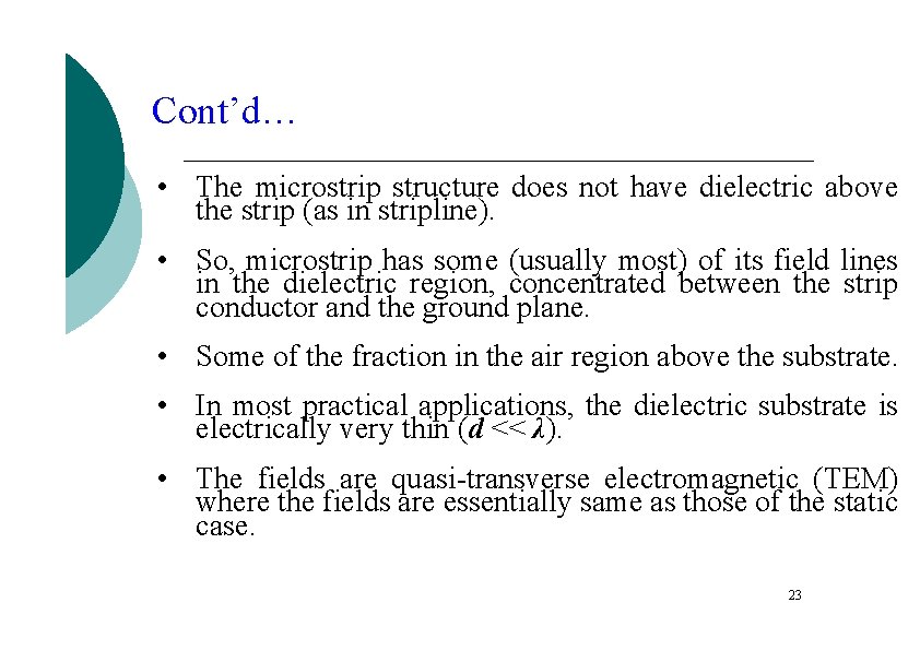
Cont’d… • The microstrip structure does not have dielectric above the strip (as in stripline). • So, microstrip has some (usually most) of its field lines in the dielectric region, concentrated between the strip conductor and the ground plane. • Some of the fraction in the air region above the substrate. • In most practical applications, the dielectric substrate is electrically very thin (d << λ). • The fields are quasi-transverse electromagnetic (TEM) where the fields are essentially same as those of the static case. 23
![Contd The phase velocity and the propagation constant 2 16 2 17 Where εe Cont’d… The phase velocity and the propagation constant: [2. 16] [2. 17] Where εe](https://slidetodoc.com/presentation_image_h/2fcaaf6ab59714b42bb6c889ce84ecbe/image-24.jpg)
Cont’d… The phase velocity and the propagation constant: [2. 16] [2. 17] Where εe is the effective dielectric constant of the microstrip line used to compensate difference between the top and bottom of the circuit line The effective dielectric constant satisfies the relation: and is dependent on the substrate thickness, d and conductor width, W. 24
![Contd The effective dielectric constant of a microstrip line is given by 2 18 Cont’d… The effective dielectric constant of a microstrip line is given by: [2. 18]](https://slidetodoc.com/presentation_image_h/2fcaaf6ab59714b42bb6c889ce84ecbe/image-25.jpg)
Cont’d… The effective dielectric constant of a microstrip line is given by: [2. 18] The effective dielectric constant can be interpreted as the dielectric consrat of a homogeneous medium that replaces the air and dielectric regions of the microstrip. Equivalent geometry of quasi-TEM microstrip line 25
![Contd The characteristic impedance can be calculated as 2 19 For a given characteristic Cont’d… The characteristic impedance can be calculated as: [2. 19] For a given characteristic](https://slidetodoc.com/presentation_image_h/2fcaaf6ab59714b42bb6c889ce84ecbe/image-26.jpg)
Cont’d… The characteristic impedance can be calculated as: [2. 19] For a given characteristic impedance, Z 0 and the dielectric constant, Єr, the W/d ratio can be found as: [2. 20] 26

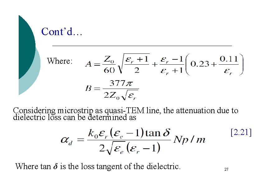
Cont’d… Where: Considering microstrip as quasi-TEM line, the attenuation due to dielectric loss can be determined as [2. 21] Where tan δ is the loss tangent of the dielectric. 27

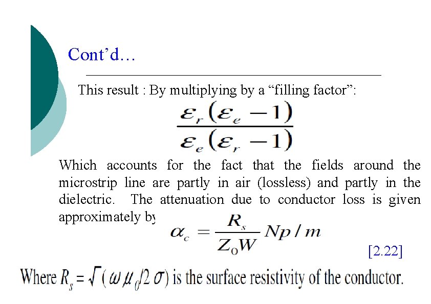
Cont’d… This result : By multiplying by a “filling factor”: Which accounts for the fact that the fields around the microstrip line are partly in air (lossless) and partly in the dielectric. The attenuation due to conductor loss is given approximately by: [2. 22]

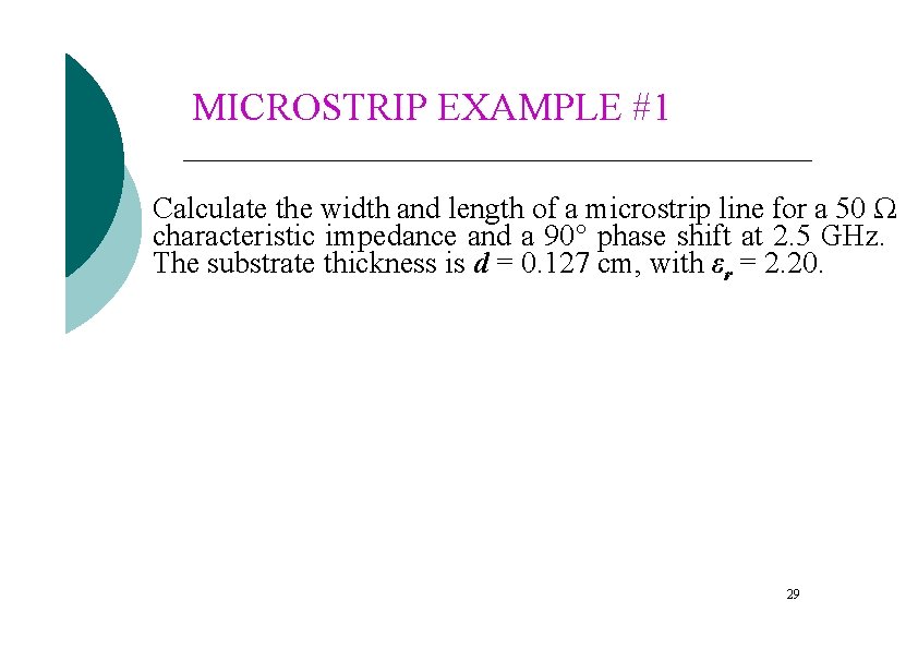
MICROSTRIP EXAMPLE #1 Calculate the width and length of a microstrip line for a 50 Ω characteristic impedance and a 90° phase shift at 2. 5 GHz. The substrate thickness is d = 0. 127 cm, with εr = 2. 20. 29

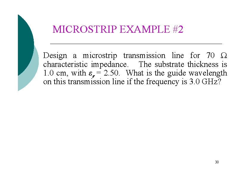
MICROSTRIP EXAMPLE #2 Design a microstrip transmission line for 70 Ω characteristic impedance. The substrate thickness is 1. 0 cm, with εr = 2. 50. What is the guide wavelength on this transmission line if the frequency is 3. 0 GHz? 30

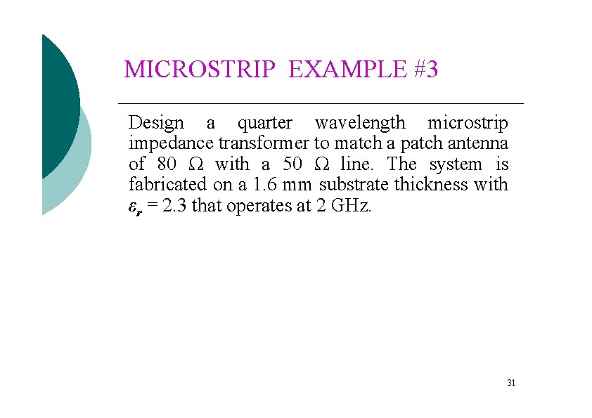
MICROSTRIP EXAMPLE #3 Design a quarter wavelength microstrip impedance transformer to match a patch antenna of 80 Ω with a 50 Ω line. The system is fabricated on a 1. 6 mm substrate thickness with εr = 2. 3 that operates at 2 GHz. 31

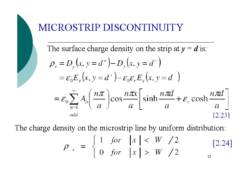
MICROSTRIP DISCONTINUITY The surface charge density on the strip at y = d is: The charge density on the microstrip line by uniform distribution: [2. 24] 32

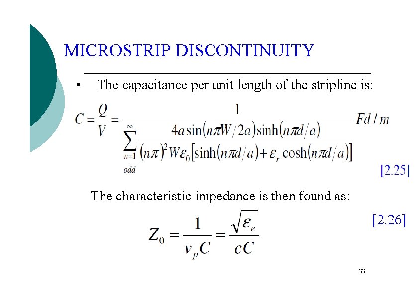
MICROSTRIP DISCONTINUITY • The capacitance per unit length of the stripline is: The characteristic impedance is then found as: [2. 26] 33

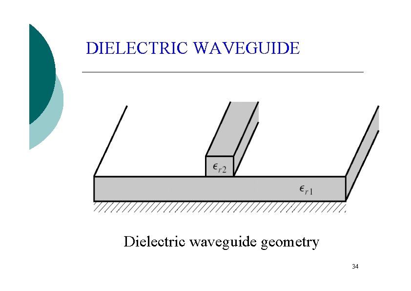
DIELECTRIC WAVEGUIDE Dielectric waveguide geometry 34

Cont’d… 35

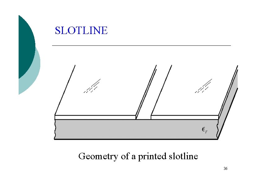
SLOTLINE Geometry of a printed slotline 36

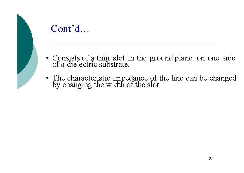
Cont’d… • Consists of a thin slot in the ground plane on one side of a dielectric substrate. • The characteristic impedance of the line can be changed by changing the width of the slot. 37
