
PGT 333 SEM II 20172018 PGT 3333 FAILURE

- Slides: 38
PGT 333 SEM II 2017/2018 PGT 333/3: FAILURE ANALYSIS Lecture 5: Fault Localization BY NURULBARIAH IDRIS
OUTLINES The Importance of Fault Localization Mechanical Probing Thermal Method Photon Emission Microscopy-PEM
What is fault localization ? finding the exact location of fault/failures in a circuit can be performed using either mechanical probing, thermal-based method, photon-based method or electron beam probing heavily dependent on the design of the IC and usually requires individuals knowledgeable about the design of the IC and the test patterns needed to stimulate the IC.
FA challenge: to locate and identify the defect, knowing only its electrical effects on the chip and perhaps secondary characteristics such as temperature and voltage sensitivity The fault can be localized to the nearest logic block or circuit net, or in some cases directly to the responsible defect’s physical location
1. The Importance of Fault Localization The most critical step in the failure analysis process is fault localization The size and complexity of modern VLSI components and defects of nanometric proportions make it imperative to accurately localize faults prior to any destructive analysis Multi-level of metallization – reduces observability and node access
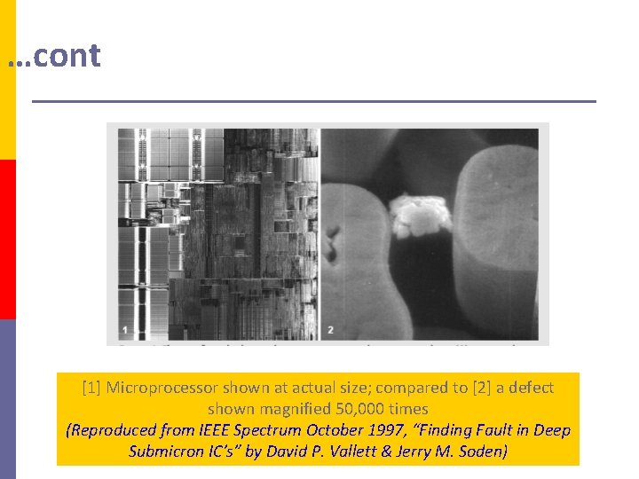
…cont [1] Microprocessor shown at actual size; compared to [2] a defect shown magnified 50, 000 times (Reproduced from IEEE Spectrum October 1997, “Finding Fault in Deep Submicron IC’s” by David P. Vallett & Jerry M. Soden)
What are the techniques available? Techniques that are generally used for failure site isolation are: (a) mechanical probing (b) thermal methods (detect defects which exhibits localized heating - hot spot or local temperature rise) (c) photon-based methods (detect defects which exhibits light) (d) electron beam-based (takes advantage of light beam ability to interact with an IC and localize the effects of this interaction)
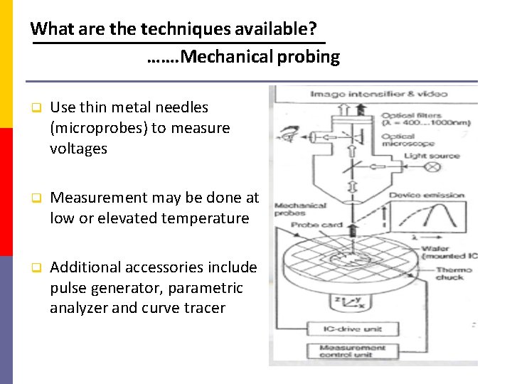
What are the techniques available? ……. Mechanical probing Use thin metal needles (microprobes) to measure voltages Measurement may be done at low or elevated temperature Additional accessories include pulse generator, parametric analyzer and curve tracer
……. Mechanical probing, making electrical contact with the feature of interest through physical contact Multiple probes can source and measure voltages and currents more precisely than any other technology. Advantages: They work reliably through a wide voltage range, can be used over a frequency range from DC to RF, can pick up transient and one-shot signals, cost much less than other probing options and make use of established, well-understood technology.
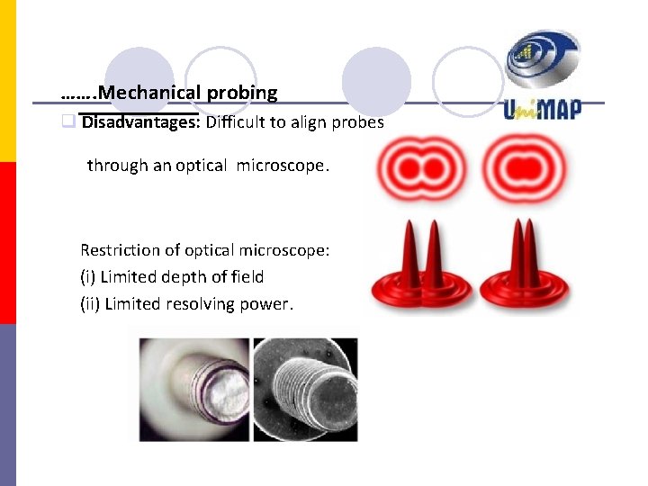
……. Mechanical probing Disadvantages: Difficult to align probes through an optical microscope. Restriction of optical microscope: (i) Limited depth of field (ii) Limited resolving power.
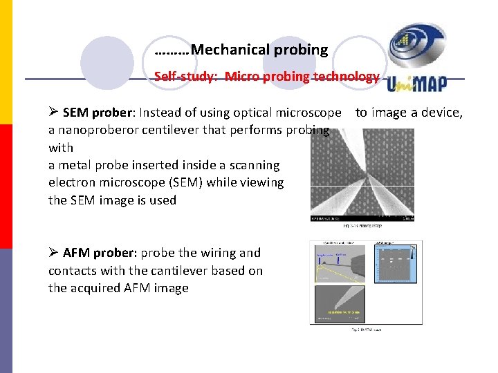
………Mechanical probing Self-study: Micro probing technology SEM prober: Instead of using optical microscope to image a device, a nanoproberor centilever that performs probing with a metal probe inserted inside a scanning electron microscope (SEM) while viewing the SEM image is used AFM prober: probe the wiring and contacts with the cantilever based on the acquired AFM image
What are the techniques available? ……. Thermal method are being used to detect defects which exhibits localized heating (hot spot or local temperature rise) Localized heating is commonly caused by lowresistance leakage paths and shorts between conductors associated with the excess current flow at the defect site
……. Thermal method Many defect types result in higher power supply currents, which generate heat during operation. Heated object emits radiation. The wavelength depends on temperature. Most of these radiation is in the infra-red. Systems to detect this power dissipation can be characterized by their sensitivity to thermal changes
……. Thermal method ……. Types of thermal techniques (a) Infrared (IR) thermal techniques - earliest available techniques that calculate the temperature of an object from its infra-red emission (b) Liquid crystals technique - provide a binary response indicating if the hot area is above the crystal’s transition temperature or not (c) Fluorescent microthermal imaging technique (FMI) - uses a scanned and focused beam from a laser to excite a thin fluorescent film disposed over the surface of the IC
………Liquid Crystal (LC) The chip (or wafer) is first placed on a temperature-controlled chuck An IC is then coated with a thin film of nematic liquid crystal and observed with polarized light while power is applied to the chip. The bias is chosen such that the defect site is allowed to conduct enough current to generate the amount of heat needed to change the visual characteristics of the liquid crystal.
………Liquid Crystal (LC) The device is heated until its surface reaches the “transition or clearing” temperature of the liquid crystal used (typicallybetween 35 and 75 °C). The device is dark as viewed with the aid of polarizing filters in the microscope. Then the temperature of the circuit is lowered until the device appears bright After powering of the device, a darkspot (hot spot) will appear where there is a defect.
Liquid Crystal Analysis The LC Analysis is used to locate heat sources associated with the electrical failure of a device By using the LC technique, one can identify failure locations caused by abnormal leakage or high power supply current in the m. A region. Under optimum conditions 10 µW can be located. Excessive heating indicates a high current flow, which may be due to die defects or abnormalities like dielectric ruptures, metallization shorts and leaky junctions
Liquid Crystal Hot Spot Detection Common materials are well defined by a melting point (0°C for water) and a boiling point (100°C for water). Nematic liquid crystals have two distinct liquid phases. The temperature dividing the two phases is called the clearing point. A test tube of liquid crystal is milky white below its clearing point but is as clear as water above its clearing point. The optical transformation (thin film) is instant and abrupt. The microscope image of an object illuminated with polarized light and viewed through a crossed polarizer is very dark, because the crossed polarizer blocks most of the light. However, a thin film of liquid crystal below its clearing point effectively twists or rotates the light as it passes through the film. The image is quite bright, because the polarizer is not crossed.
…contd An IC coated with a thin film of liquid crystal and viewed through crossed polarizers appears mottled and bright. If a spot of liquid crystal is locally heated above the clearing point temperature, that spot will become instantly black. Depending on ambient temperature, 20 to 30 m. W of power may be required to create a discernible spot. If the ambient temperature is increased to a temperature just below the clearing point, 10 to 100 µW may be enough to produce a visible hot spot.
Device Failure Characteristics Whenever a failure is characterized by abnormal leakage or high power supply current, liquid crystal hot spot detection is an appropriate technique. The only circuit knowledge required is how to bias the device in the abnormally high current state. The procedure is simplest when the leakage is between two pins such as input and ground, or VDD and VSS. In such two pin cases, any hot spots detected are associated with the failure. Liquid crystal is also effective when the circuit must be specifically biased to address the high current state. Digital devices that fail IDDQ in specific logic states are perfect candidates for liquid crystal analysis.
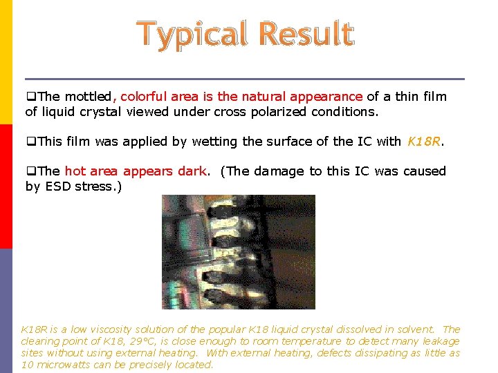
Typical Result The mottled, colorful area is the natural appearance of a thin film of liquid crystal viewed under cross polarized conditions. This film was applied by wetting the surface of the IC with K 18 R. The hot area appears dark. (The damage to this IC was caused by ESD stress. ) K 18 R is a low viscosity solution of the popular K 18 liquid crystal dissolved in solvent. The clearing point of K 18, 29°C, is close enough to room temperature to detect many leakage sites without using external heating. With external heating, defects dissipating as little as 10 microwatts can be precisely located.
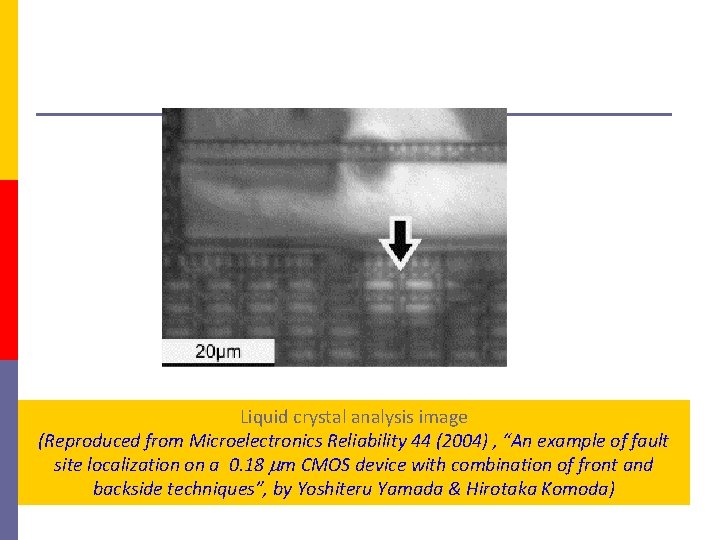
Liquid crystal analysis image (Reproduced from Microelectronics Reliability 44 (2004) , “An example of fault site localization on a 0. 18 m CMOS device with combination of front and backside techniques”, by Yoshiteru Yamada & Hirotaka Komoda)
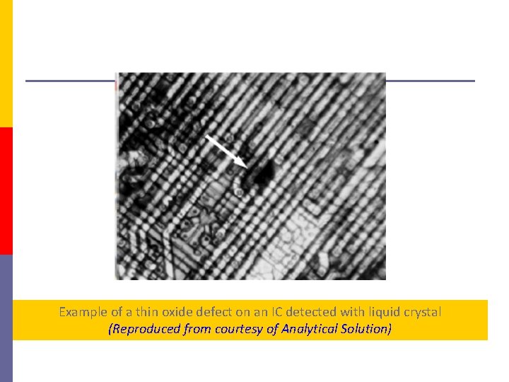
Example of a thin oxide defect on an IC detected with liquid crystal (Reproduced from courtesy of Analytical Solution)
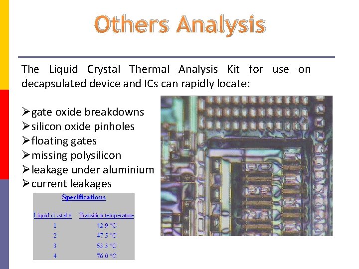
Others Analysis The Liquid Crystal Thermal Analysis Kit for use on decapsulated device and ICs can rapidly locate: gate oxide breakdowns silicon oxide pinholes floating gates missing polysilicon leakage under aluminium current leakages
Question 1 What are the equipment considerations during LC analysis?
Answer 1 - Metallurgical Microscope - Curve Tracer - Additional Power Supply - External Heating Device - Variable Power Switch - Video Camera & Monitor - Video Capture Capability
……. Thermal method ……. Types of photon-based ………Photon-based Photoemission microscopy, or light emission microscopy (LEM), is a relatively new failure analysis technique for detecting photonic radiation from a defect site, primarily due to carrier recombination mechanisms Well known method to analyze current leaks - involve extremely feeble photoemissions produced by hot electrons and the recombination of minority carriers.
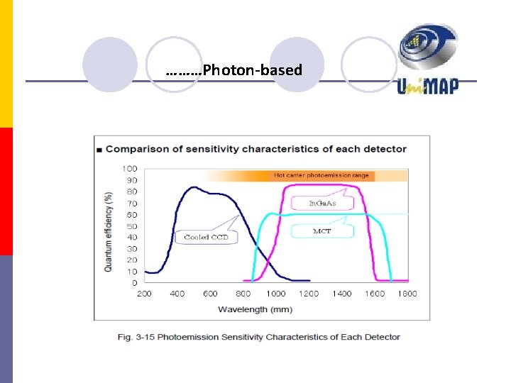
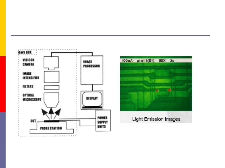
………Photon-based Such light / photo emissions are not visible to the naked eye. PEM therefore involves the use a powerful image intensification technology to amplify the light emitted by such defect sites An an ultra-high-sensitivity cooled CCD camera (effective sensitivity approximately 200 nm to 1000 nm) and creating images of the semiconductor device circuit location where the photoemission is occurring
………Photon-based Recently, MCT cameras that have improved sensitivity in the infrared wavelength range and new-type In. Ga. As cameras (effective sensitivity approximately 800 nm to 2000 nm) have also appeared. Advantages: (i) extremely good sensitivity characteristics in the infrared range (ii) highly effective at capturing photoemissions from the rear surface of the chip (handy when dealing with multilayer wiring)
………Photon-based
Photon Emission Microscopy-PEM Some defect sites emit light during operation (which signify high current and reverse biased breakdown) which would otherwise be absent in a normal device Photoemission microscopy, or light emission microscopy (LEM), is a relatively new failure analysis technique for detecting photonic radiation from a defect site, primarily due to carrier recombination mechanisms
Photon emission is typically a result of direct recombination of electron-hole pairs, thus defects with leakage profile will enhance further the recombination process Such light / photo emissions are not visible to the naked eye PEM therefore involves in collecting and imaging the light given off from these ICs
In general, photoemission microscopy uses a powerful image intensification technology to amplify the light emitted by such defect sites, therefore useful in locating defects that exhibit light emissions
Photoemission microscopy applications include but are not limited to the following : 1) detection of previously unknown or undetectable electroluminescence; 2) detection of avalanche luminescence from junction breakdowns, junction defects, currents due to saturated MOS transistors, and transistor hot electron effects; 3) detection of dielectric electroluminescence from current flow through Si. O 2 and Si. N.
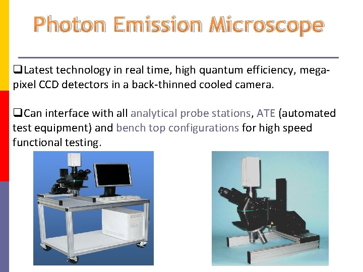
Photon Emission Microscope Latest technology in real time, high quantum efficiency, megapixel CCD detectors in a back-thinned cooled camera. Can interface with all analytical probe stations, ATE (automated test equipment) and bench top configurations for high speed functional testing.
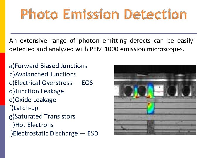
Photo Emission Detection An extensive range of photon emitting defects can be easily detected analyzed with PEM 1000 emission microscopes. a)Forward Biased Junctions b)Avalanched Junctions c)Electrical Overstress — EOS d)Junction Leakage e)Oxide Leakage f)Latch-up g)Saturated Transistors h)Hot Electrons i)Electrostatic Discharge — ESD
Conclusion Fault localization is important to localize defects so that the location of failures can be determined Different types of fault localization method available: mechanical probing thermal analysis photoemission analysis electron-beam based Cares should be taken when interpreting data obtained from the fault localization method.