Introduction to Nanoelectronics EE 315 ECE 451 Ryan

- Slides: 25

Introduction to Nanoelectronics EE 315 / ECE 451 Ryan Munden Fairfield University BNW 105, x 2764 rmunden@fairfield. edu

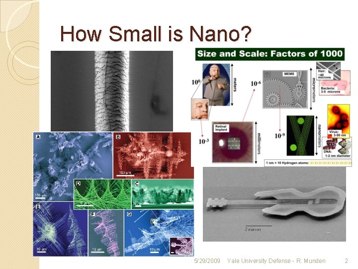
How Small is Nano? 5/29/2009 Yale University Defense - R. Munden 2

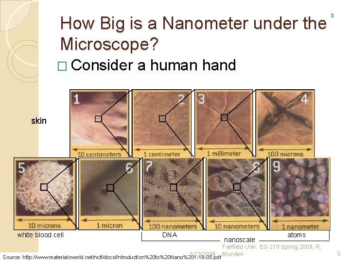
3 How Big is a Nanometer under the Microscope? � Consider a human hand skin white blood cell DNA nanoscale 1/13/2009 Source: http: //www. materialsworld. net/nclt/docs/Introduction%20 to%20 Nano%201 -18 -05. pdf atoms Fairfield Univ. EG 210 Spring 2009, R. Munden 3

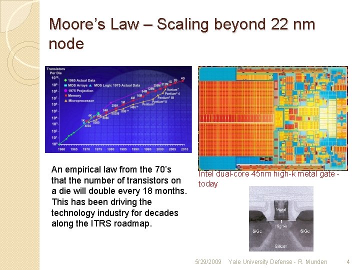
Moore’s Law – Scaling beyond 22 nm node An empirical law from the 70’s Intel dual-core 45 nm high-k metal gate - that the number of transistors on today a die will double every 18 months. This has been driving the technology industry for decades along the ITRS roadmap. 5/29/2009 Yale University Defense - R. Munden 4

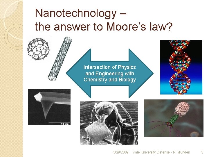
Nanotechnology – the answer to Moore’s law? Intersection of Physics and Engineering with Chemistry and Biology 5/29/2009 Yale University Defense - R. Munden 5

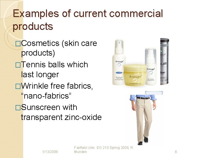
Examples of current commercial products �Cosmetics (skin care products) �Tennis balls which last longer �Wrinkle free fabrics, “nano-fabrics” �Sunscreen with transparent zinc-oxide 1/13/2009 Fairfield Univ. EG 210 Spring 2009, R. Munden 6

Impact of Nanotechnology on Global Economy Between 1997 and 2005, governments around the world invested from $432 million to about $4. 1 billion in nanotech research and development, and by 2005 private funding exceeded government funding. By 2015 it is estimated that nanotech products will contribute approx. $1 trillion to the global economy, with about 2 million workers employed in nanotech industries and 3 X that many in supporting jobs (Roco, 2006). 1/13/2009 Fairfield Univ. EG 210 Spring 2009, R. Munden 7

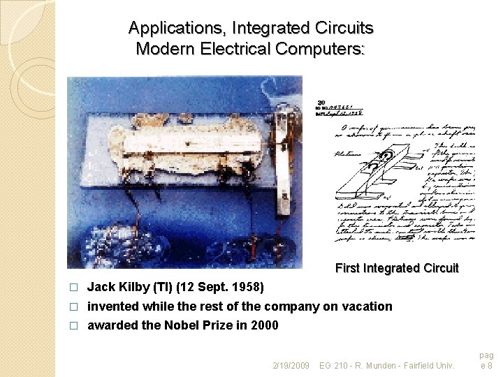
Applications, Integrated Circuits Modern Electrical Computers: First Integrated Circuit � Jack Kilby (TI) (12 Sept. 1958) � invented while the rest of the company on vacation � awarded the Nobel Prize in 2000 2/19/2009 EG 210 - R. Munden - Fairfield Univ. pag e 8

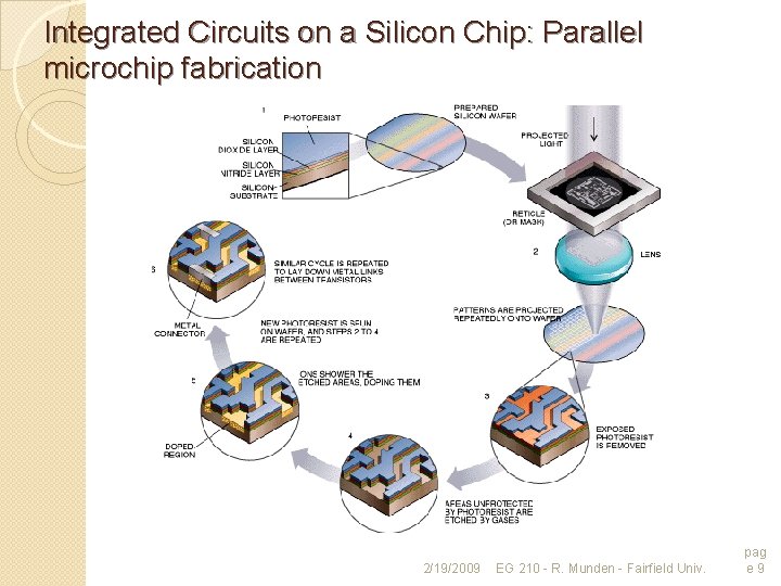
Integrated Circuits on a Silicon Chip: Parallel microchip fabrication 2/19/2009 EG 210 - R. Munden - Fairfield Univ. pag e 9

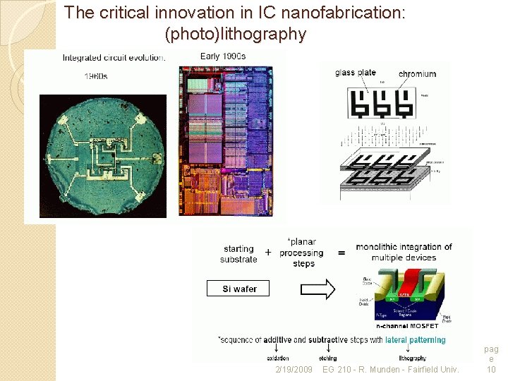
The critical innovation in IC nanofabrication: (photo)lithography 2/19/2009 EG 210 - R. Munden - Fairfield Univ. pag e 10

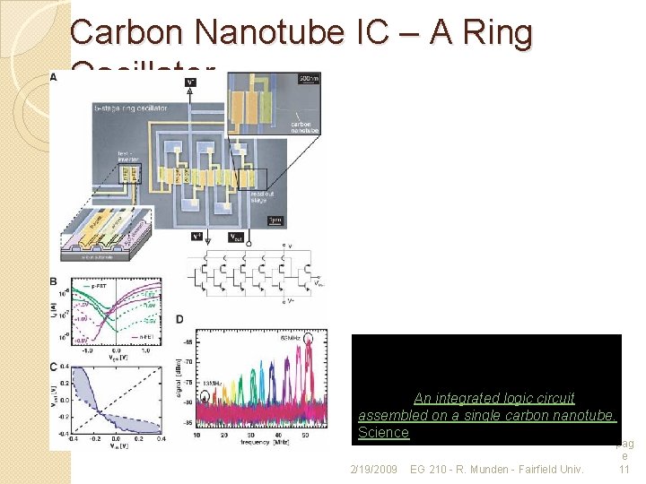
Carbon Nanotube IC – A Ring Oscillator Z. H. Chen, J. Appenzeller, Y. M. Lin, J. Sippel-Oakley, A. G. Rinzler, J. Y. Tang, S. J. Wind, P. M. Solomon, and P. Avouris, An integrated logic circuit assembled on a single carbon nanotube. Science, 311, 1735 (2006). 2/19/2009 EG 210 - R. Munden - Fairfield Univ. pag e 11

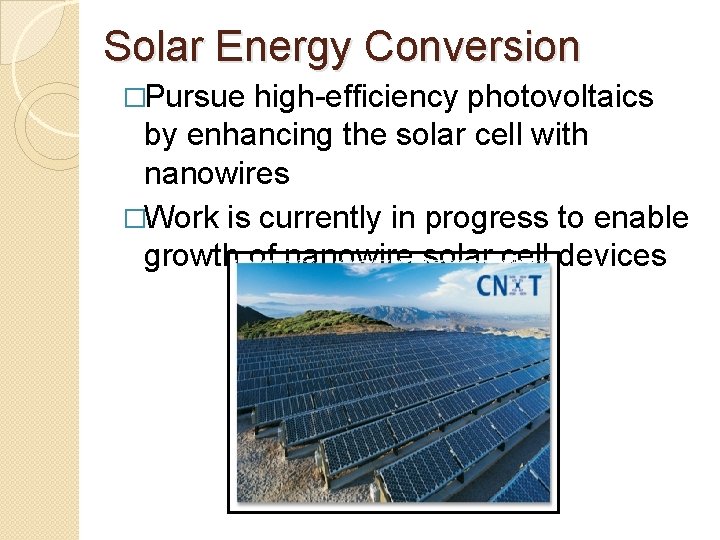
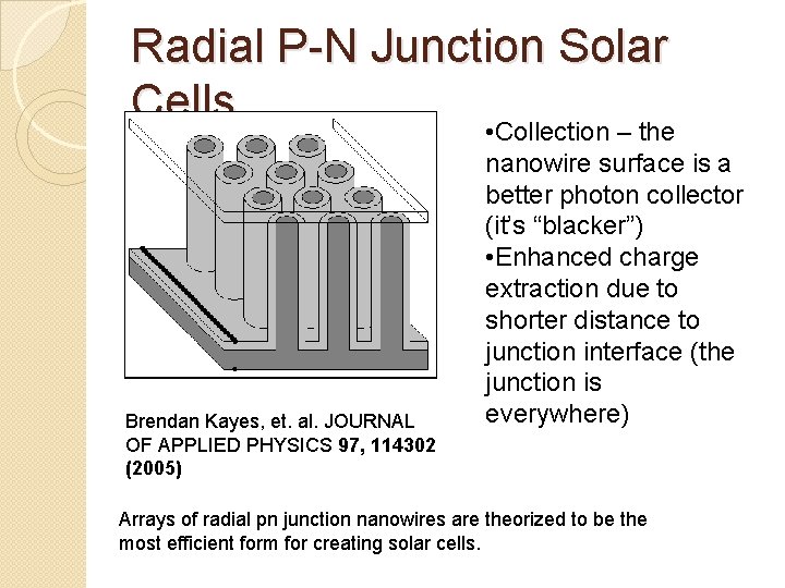
Solar Energy Conversion �Pursue high-efficiency photovoltaics by enhancing the solar cell with nanowires �Work is currently in progress to enable growth of nanowire solar cell devices

Radial P-N Junction Solar Cells • Collection – the Brendan Kayes, et. al. JOURNAL OF APPLIED PHYSICS 97, 114302 (2005) nanowire surface is a better photon collector (it’s “blacker”) • Enhanced charge extraction due to shorter distance to junction interface (the junction is everywhere) Arrays of radial pn junction nanowires are theorized to be the most efficient form for creating solar cells.

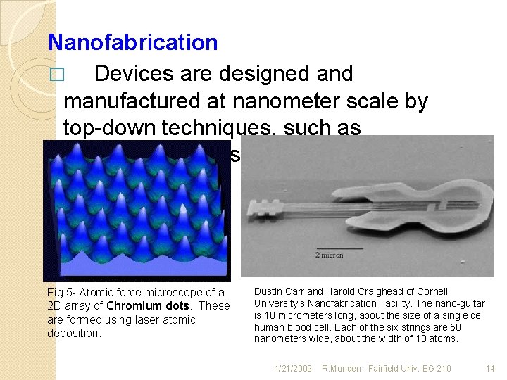
Nanofabrication � Devices are designed and manufactured at nanometer scale by top-down techniques, such as lithography, or laser deposition Fig 5 - Atomic force microscope of a 2 D array of Chromium dots. These are formed using laser atomic deposition. Dustin Carr and Harold Craighead of Cornell University’s Nanofabrication Facility. The nano-guitar is 10 micrometers long, about the size of a single cell human blood cell. Each of the six strings are 50 nanometers wide, about the width of 10 atoms. 1/21/2009 R. Munden - Fairfield Univ. EG 210 14

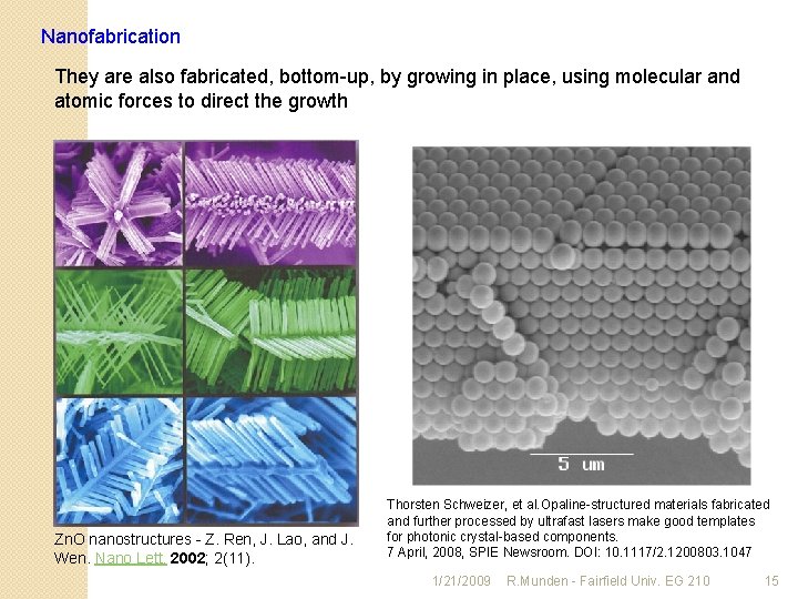
Nanofabrication They are also fabricated, bottom-up, by growing in place, using molecular and atomic forces to direct the growth Zn. O nanostructures - Z. Ren, J. Lao, and J. Wen. Nano Lett. 2002; 2(11). Thorsten Schweizer, et al. Opaline-structured materials fabricated and further processed by ultrafast lasers make good templates for photonic crystal-based components. 7 April, 2008, SPIE Newsroom. DOI: 10. 1117/2. 1200803. 1047 1/21/2009 R. Munden - Fairfield Univ. EG 210 15

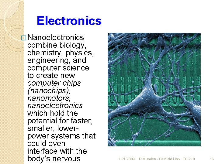
Electronics � Nanoelectronics combine biology, chemistry, physics, engineering, and computer science to create new computer chips (nanochips), nanomotors, nanoelectronics which hold the potential for faster, smaller, lowerpower systems that could even interface with the body’s nervous 1/21/2009 R. Munden - Fairfield Univ. EG 210 16

Thank You!

Why do we care about nanowires? �Bottom up electronic device fabrication �Integration of heterostructure (i. e. III- V) devices into CMOS processes �Sensing applications, high Surface-to. Volume ratio �Photonics, active optical elements, plasmon waveguides, efficient solar cells �May exhibit quasi-1 D transport for interesting physics, memory, nanoelectronics 5/29/2009 Yale University Defense - R. Munden 18

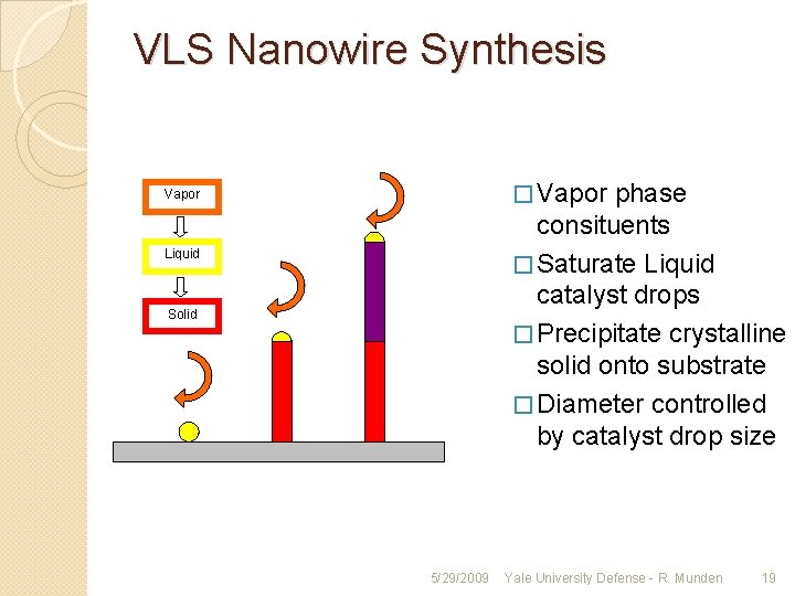
VLS Nanowire Synthesis � Vapor phase Vapor consituents � Saturate Liquid catalyst drops � Precipitate crystalline solid onto substrate � Diameter controlled by catalyst drop size Liquid Solid 5/29/2009 Yale University Defense - R. Munden 19

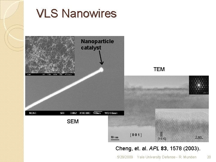
VLS Nanowires Nanoparticle catalyst TEM SEM Cheng, et. al. APL 83, 1578 (2003). 5/29/2009 Yale University Defense - R. Munden 20

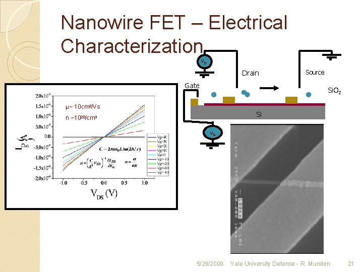
Nanowire FET – Electrical Characterization VD Drain Gate Source Si. O 2 μ~ 10 cm 2/Vs Si n ~1020/cm 3 VG 5/29/2009 Yale University Defense - R. Munden 21

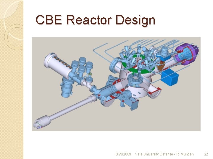
CBE Reactor Design 5/29/2009 Yale University Defense - R. Munden 22

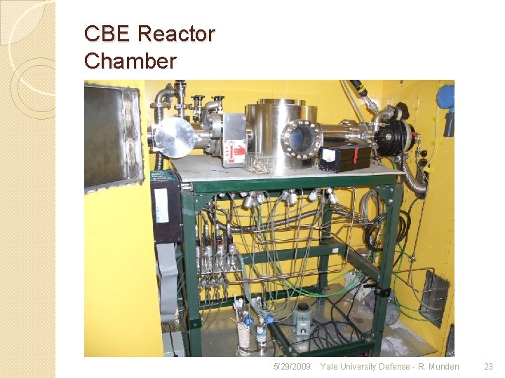
CBE Reactor Chamber 5/29/2009 Yale University Defense - R. Munden 23

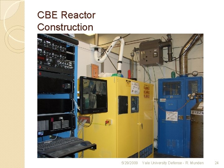
CBE Reactor Construction 5/29/2009 Yale University Defense - R. Munden 24

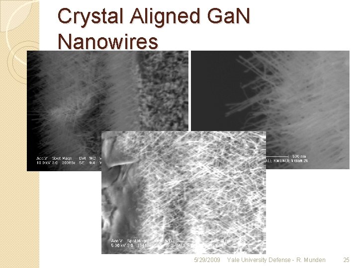
Crystal Aligned Ga. N Nanowires 5/29/2009 Yale University Defense - R. Munden 25