Nanoelectronics Synthesis and Applications of Semiconductor Nanowires Group
- Slides: 31
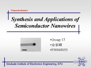
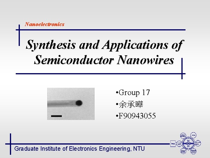
Nanoelectronics Synthesis and Applications of Semiconductor Nanowires • Group 17 • 余承曄 • F 90943055 Graduate Institute of Electronics Engineering, NTU
Outline Nanoelectronics v. Synthesis of semiconductor nanowires v Electrical device v Optical device v Nanowire sensor Graduate Institute of Electronics Engineering, NTU
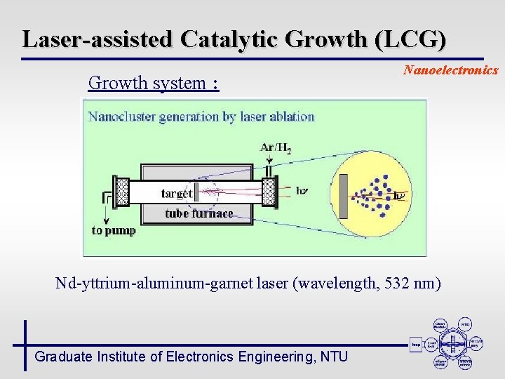
Laser-assisted Catalytic Growth (LCG) Growth system : Nanoelectronics Nd-yttrium-aluminum-garnet laser (wavelength, 532 nm) Graduate Institute of Electronics Engineering, NTU
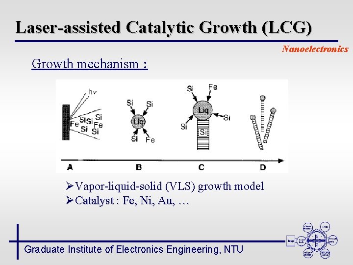
Laser-assisted Catalytic Growth (LCG) Nanoelectronics Growth mechanism : ØVapor-liquid-solid (VLS) growth model ØCatalyst : Fe, Ni, Au, … Graduate Institute of Electronics Engineering, NTU
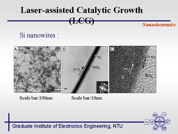
Laser-assisted Catalytic Growth (LCG) Nanoelectronics Si nanowires : Scale bar: 100 nm Scale bar: 10 nm Graduate Institute of Electronics Engineering, NTU
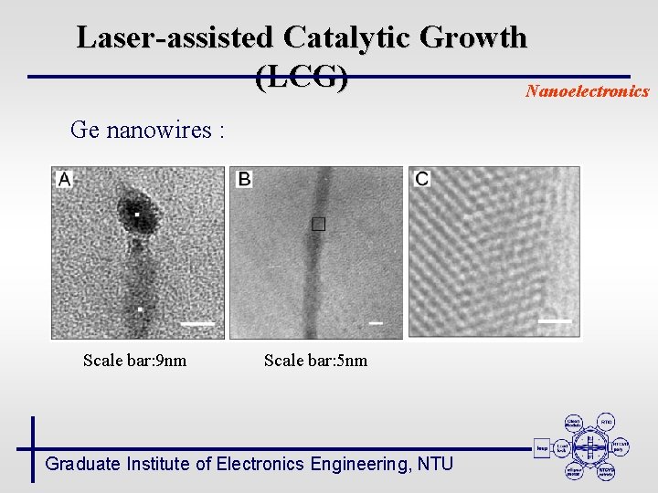
Laser-assisted Catalytic Growth (LCG) Nanoelectronics Ge nanowires : Scale bar: 9 nm Scale bar: 5 nm Graduate Institute of Electronics Engineering, NTU
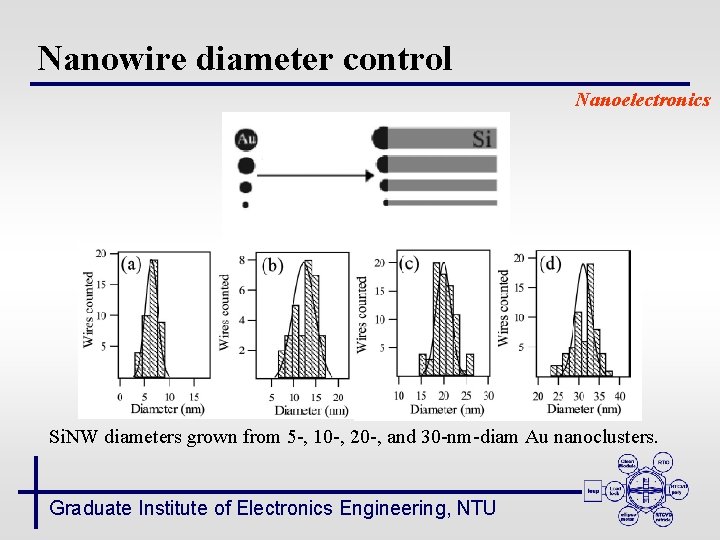
Nanowire diameter control Nanoelectronics Si. NW diameters grown from 5 -, 10 -, 20 -, and 30 -nm-diam Au nanoclusters. Graduate Institute of Electronics Engineering, NTU
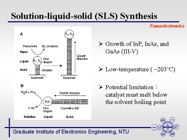
Solution-liquid-solid (SLS) Synthesis Nanoelectronics Ø Growth of In. P, In. As, and Ga. As (III-V) Ø Low-temperature ( ~203°C) Ø Potential limitation: catalyst must melt below the solvent boiling point Graduate Institute of Electronics Engineering, NTU
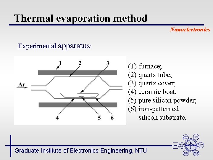
Thermal evaporation method Nanoelectronics Experimental apparatus: (1) furnace; (2) quartz tube; (3) quartz cover; (4) ceramic boat; (5) pure silicon powder; (6) iron-patterned silicon substrate. Graduate Institute of Electronics Engineering, NTU
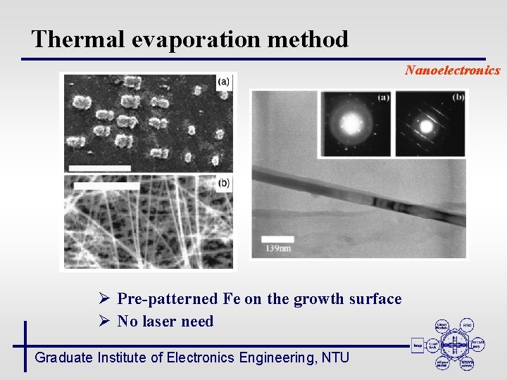
Thermal evaporation method Nanoelectronics Ø Pre-patterned Fe on the growth surface Ø No laser need Graduate Institute of Electronics Engineering, NTU
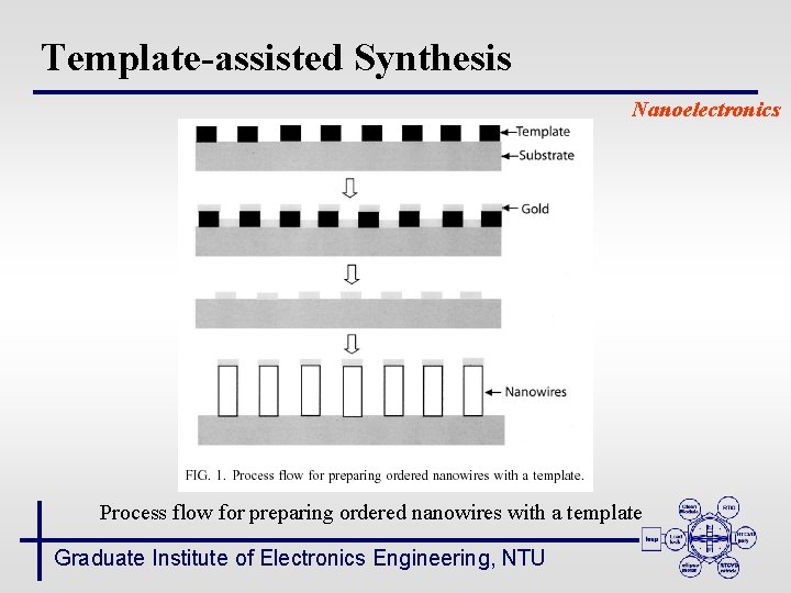
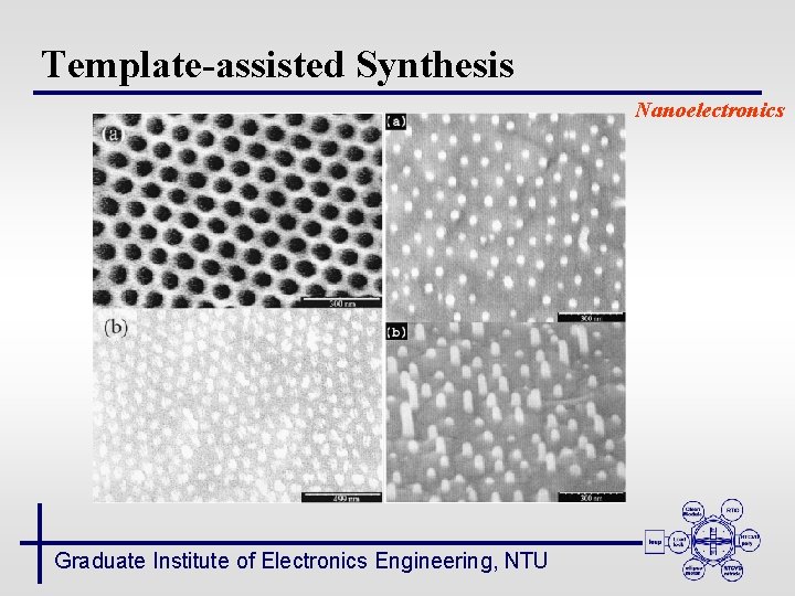
Template-assisted Synthesis Nanoelectronics Process flow for preparing ordered nanowires with a template Graduate Institute of Electronics Engineering, NTU
Template-assisted Synthesis Nanoelectronics Graduate Institute of Electronics Engineering, NTU
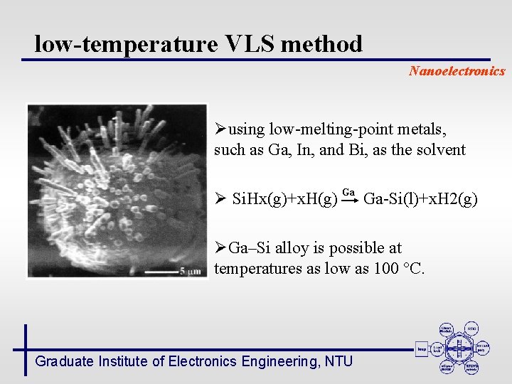
low-temperature VLS method Nanoelectronics Øusing low-melting-point metals, such as Ga, In, and Bi, as the solvent Ø Si. Hx(g)+x. H(g) Ga Ga-Si(l)+x. H 2(g) ØGa–Si alloy is possible at temperatures as low as 100 °C. Graduate Institute of Electronics Engineering, NTU
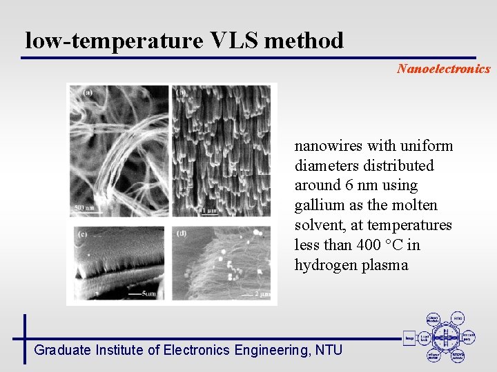
low-temperature VLS method Nanoelectronics nanowires with uniform diameters distributed around 6 nm using gallium as the molten solvent, at temperatures less than 400 °C in hydrogen plasma Graduate Institute of Electronics Engineering, NTU
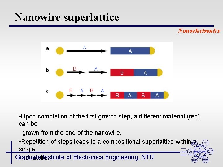
Nanowire superlattice Nanoelectronics • Upon completion of the first growth step, a different material (red) can be grown from the end of the nanowire. • Repetition of steps leads to a compositional superlattice within a single Graduate Institute of Electronics Engineering, NTU nanowire.
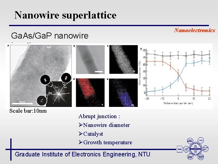
Nanowire superlattice Ga. As/Ga. P nanowire junctions Scale bar: 10 nm Abrupt junction : ØNanowire diameter ØCatalyst ØGrowth temperature Graduate Institute of Electronics Engineering, NTU Nanoelectronics
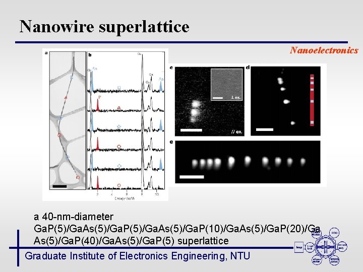
Nanowire superlattice Nanoelectronics a 40 -nm-diameter Ga. P(5)/Ga. As(5)/Ga. P(10)/Ga. As(5)/Ga. P(20)/Ga As(5)/Ga. P(40)/Ga. As(5)/Ga. P(5) superlattice Graduate Institute of Electronics Engineering, NTU
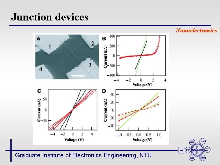
Junction devices Nanoelectronics Graduate Institute of Electronics Engineering, NTU
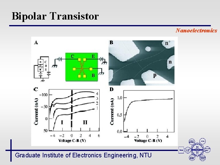
Bipolar Transistor Nanoelectronics Graduate Institute of Electronics Engineering, NTU
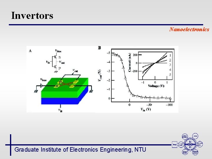
Invertors Nanoelectronics Graduate Institute of Electronics Engineering, NTU
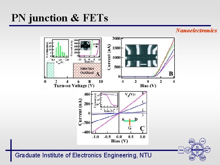
PN junction & FETs Nanoelectronics Graduate Institute of Electronics Engineering, NTU
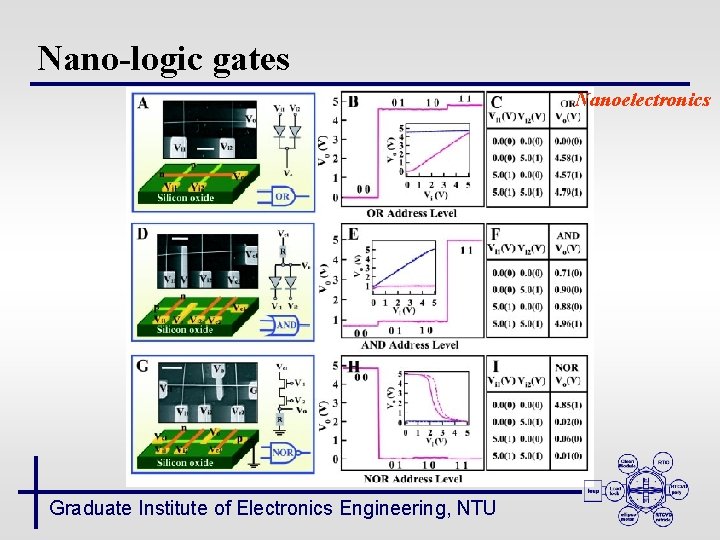
Nano-logic gates Nanoelectronics Graduate Institute of Electronics Engineering, NTU
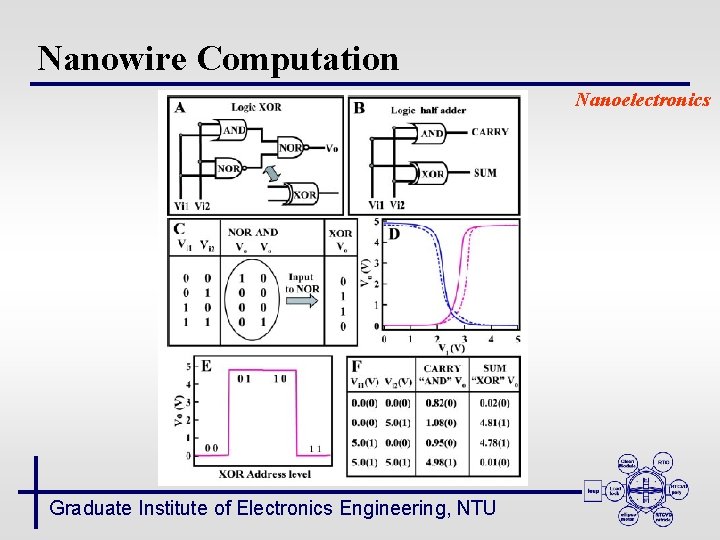
Nanowire Computation Nanoelectronics Graduate Institute of Electronics Engineering, NTU
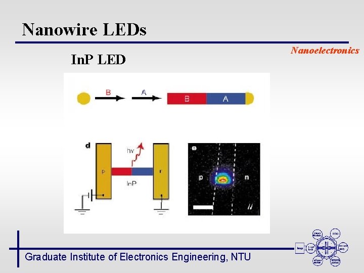
Nanowire LEDs In. P LED Graduate Institute of Electronics Engineering, NTU Nanoelectronics
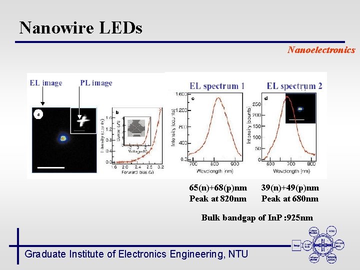
Nanowire LEDs Nanoelectronics 65(n)+68(p)nm Peak at 820 nm 39(n)+49(p)nm Peak at 680 nm Bulk bandgap of In. P : 925 nm Graduate Institute of Electronics Engineering, NTU
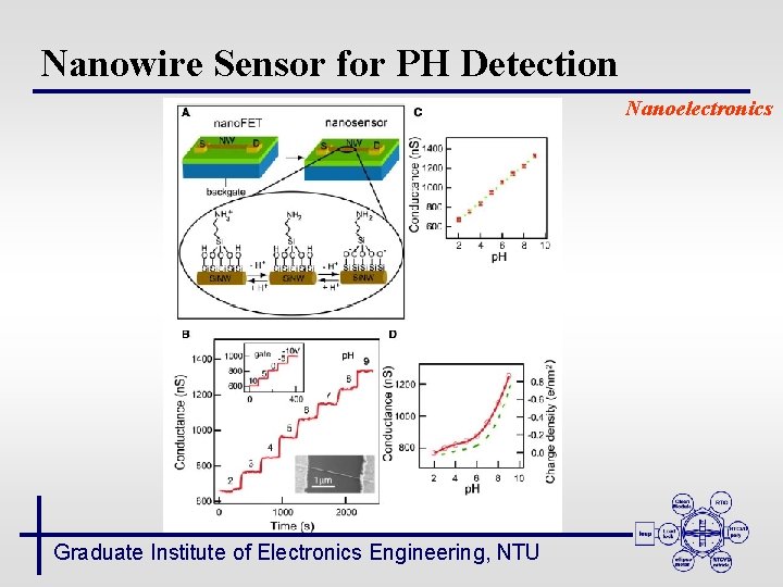
Nanowire Sensor for PH Detection Nanoelectronics Graduate Institute of Electronics Engineering, NTU
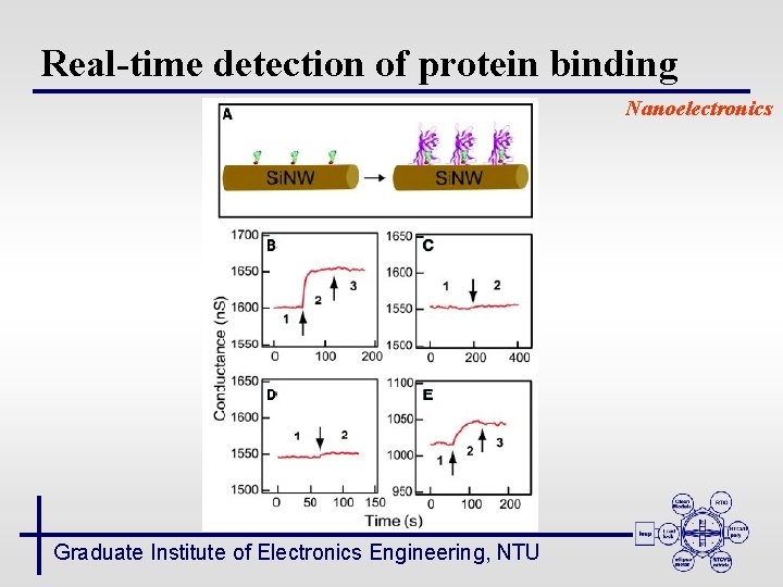
Real-time detection of protein binding Nanoelectronics Graduate Institute of Electronics Engineering, NTU
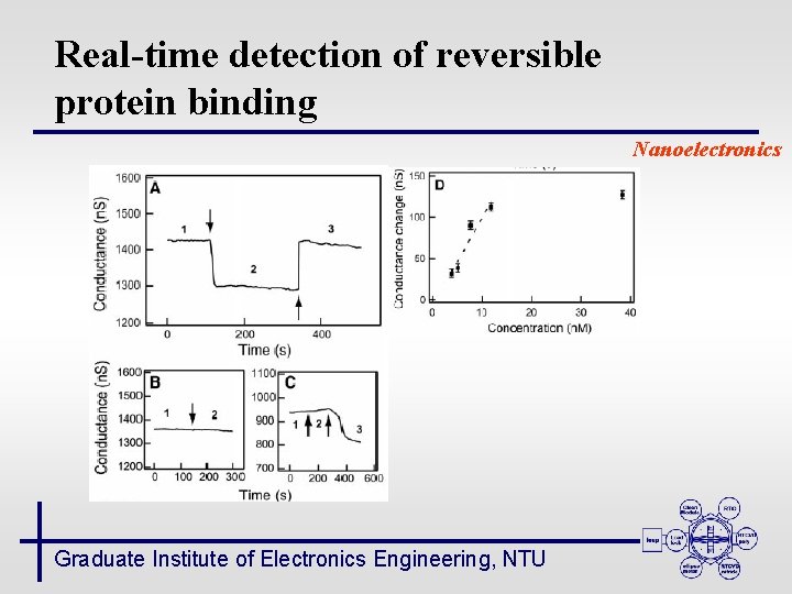
Real-time detection of reversible protein binding Nanoelectronics Graduate Institute of Electronics Engineering, NTU
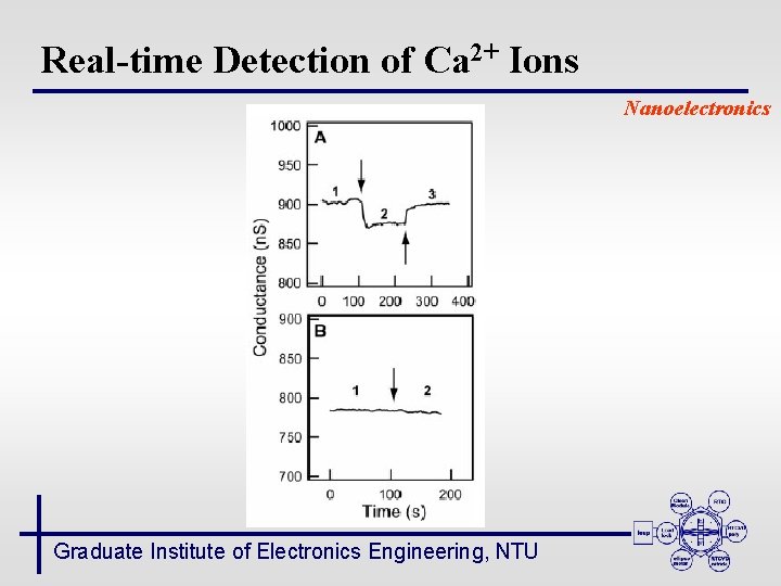
Real-time Detection of Ca 2+ Ions Nanoelectronics Graduate Institute of Electronics Engineering, NTU
References Nanoelectronics 1. A. M. Morales and C. M. Lieber, Science 279, 210 (1998). 2. M. S. Gudiksen et al. , Nature 415, 617 (2002). 3. B. H. Hong et al. , Science 294, 348 (2001). 4. T. Thurn-Albrecht et al. , Science 290, 2126 (2000) 5. A. J. Yin et al. , Applied Physics Letters 79, 1039 (2001). 6. M. Paulose et al. , Applied Physics Letters 81, 153 (2002). 7. Y. Cui and C. M. Lieber, Science 291, 851 (2001). 8. Y. Huang et al. , Science 294, 1313 (2001). 9. Y. Cui et al. , Science 293, 1289 (2001). Graduate Institute of Electronics Engineering, NTU
References Nanoelectronics 10. M. K. Sunkara et al. , Applied Physics Letters 79, 1546 (2001). 11. T. J. Trentlor et al. , Science 270, 1791 (1995) 12. Yi Cui et al. , Applied Physics Letters 78, 2214 (2001). 13. Z. H. Wu et al. , Applied Physics Letters 81, 5177 (2002). 14. Qian Gu et al. , Applied Physics Letters 76, 3020 (2000). Graduate Institute of Electronics Engineering, NTU