Teaching Nanoelectronics Paolo Lugli Institute for Nanoelectronics Munich
- Slides: 47
Teaching Nanoelectronics Paolo Lugli Institute for Nanoelectronics Munich, Germany
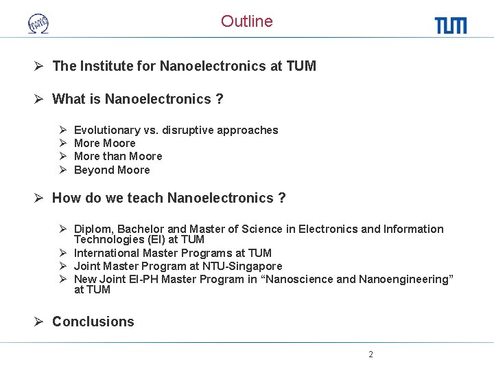
Outline Ø The Institute for Nanoelectronics at TUM Ø What is Nanoelectronics ? Ø Ø Evolutionary vs. disruptive approaches More than Moore Beyond Moore Ø How do we teach Nanoelectronics ? Ø Diplom, Bachelor and Master of Science in Electronics and Information Technologies (EI) at TUM Ø International Master Programs at TUM Ø Joint Master Program at NTU-Singapore Ø New Joint EI-PH Master Program in “Nanoscience and Nanoengineering” at TUM Ø Conclusions 2
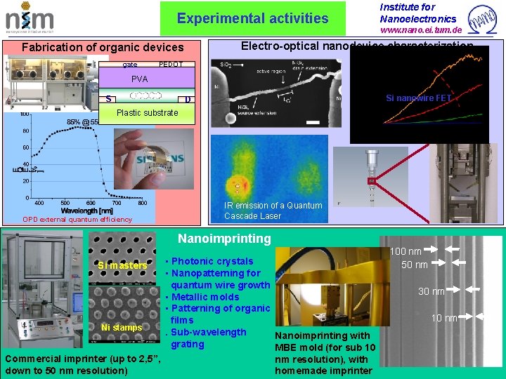
Experimental activities www. nano. ei. tum. de Electro-optical nanodevice characterization Fabrication of organic devices gate Institute for Nanoelectronics PEDOT PVA S Si nanowire FET D Plastic substrate OPD external quantum efficiency IR emission of a Quantum Cascade Laser Nanoimprinting • Photonic crystals • Nanopatterning for quantum wire growth • Metallic molds • Patterning of organic films Ni stamps. Sub-wavelength Nanoimprinting with grating MBE mold (for sub 10 Commercial imprinter (up to 2, 5”, nm resolution), with down to 50 nm resolution) homemade imprinter Si masters 100 nm 50 nm 30 nm 10 nm
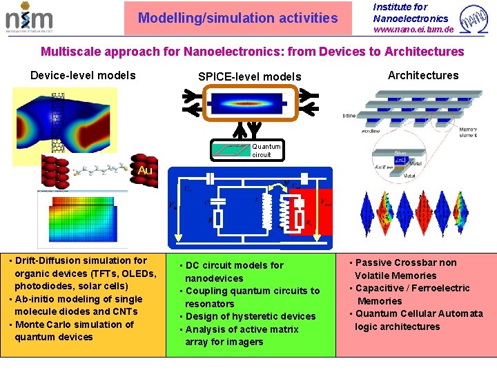
Modelling/simulation activities Institute for Nanoelectronics www. nano. ei. tum. de Multiscale approach for Nanoelectronics: from Devices to Architectures Device-level models SPICE-level models Architectures Quantum circuit Au • Drift-Diffusion simulation for organic devices (TFTs, OLEDs, photodiodes, solar cells) • Ab-initio modeling of single molecule diodes and CNTs • Monte Carlo simulation of quantum devices • DC circuit models for nanodevices • Coupling quantum circuits to resonators • Design of hysteretic devices • Analysis of active matrix array for imagers • Passive Crossbar non Volatile Memories • Capacitive / Ferroelectric Memories • Quantum Cellular Automata logic architectures
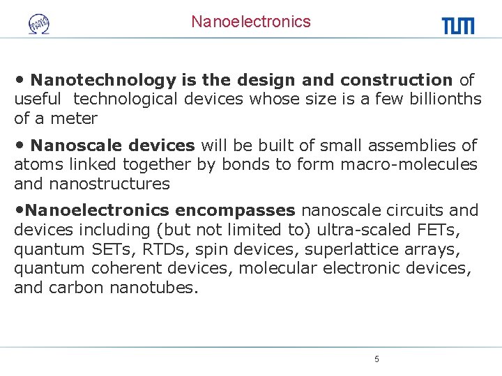
Nanoelectronics • Nanotechnology is the design and construction of useful technological devices whose size is a few billionths of a meter • Nanoscale devices will be built of small assemblies of atoms linked together by bonds to form macro-molecules and nanostructures • Nanoelectronics encompasses nanoscale circuits and devices including (but not limited to) ultra-scaled FETs, quantum SETs, RTDs, spin devices, superlattice arrays, quantum coherent devices, molecular electronic devices, and carbon nanotubes. 5
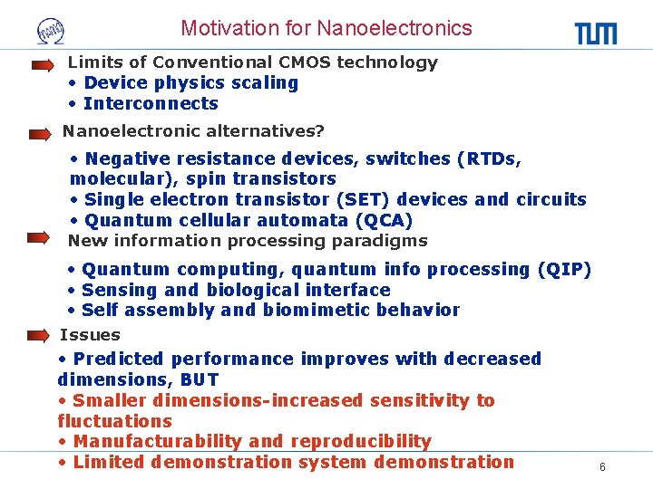
Motivation for Nanoelectronics Limits of Conventional CMOS technology • Device physics scaling • Interconnects Nanoelectronic alternatives? • Negative resistance devices, switches (RTDs, molecular), spin transistors • Single electron transistor (SET) devices and circuits • Quantum cellular automata (QCA) New information processing paradigms • Quantum computing, quantum info processing (QIP) • Sensing and biological interface • Self assembly and biomimetic behavior Issues • Predicted performance improves with decreased dimensions, BUT • Smaller dimensions-increased sensitivity to fluctuations • Manufacturability and reproducibility • Limited demonstration system demonstration 6
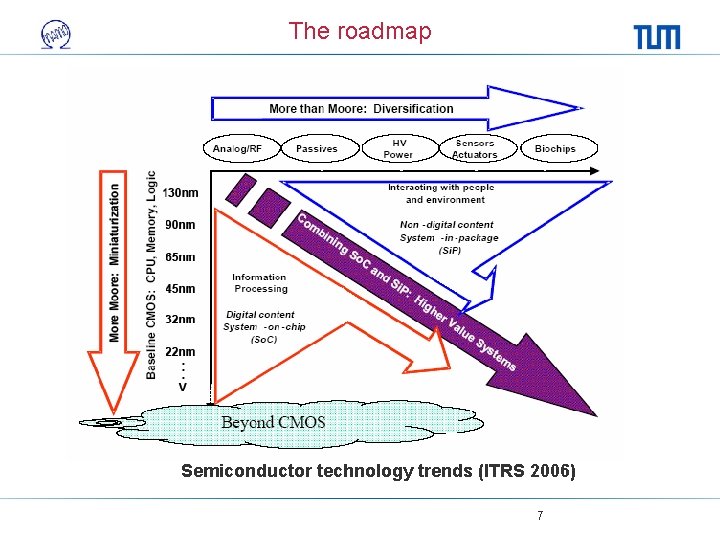
The roadmap Semiconductor technology trends (ITRS 2006) 7
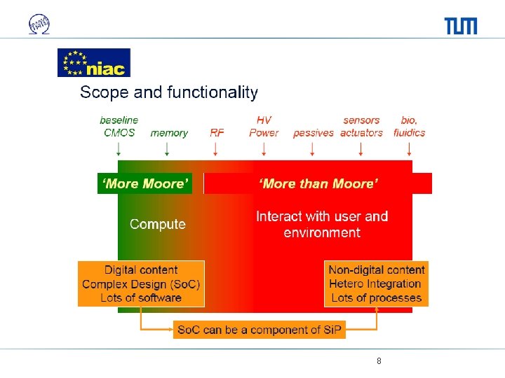
8
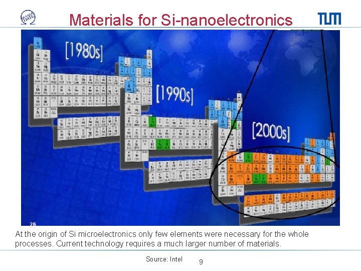
Materials for Si-nanoelectronics At the origin of Si microelectronics only few elements were necessary for the whole processes. Current technology requires a much larger number of materials. Source: Intel 9
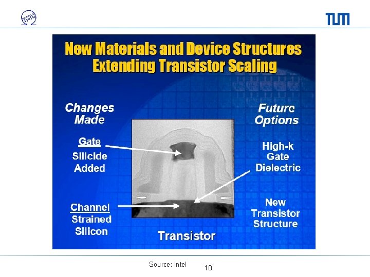
Source: Intel 10
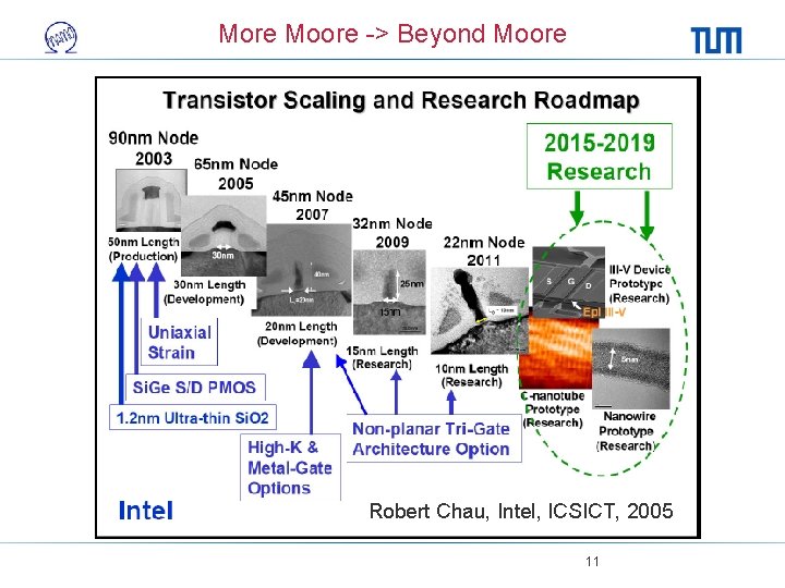
More Moore -> Beyond Moore Robert Chau, Intel, ICSICT, 2005 11
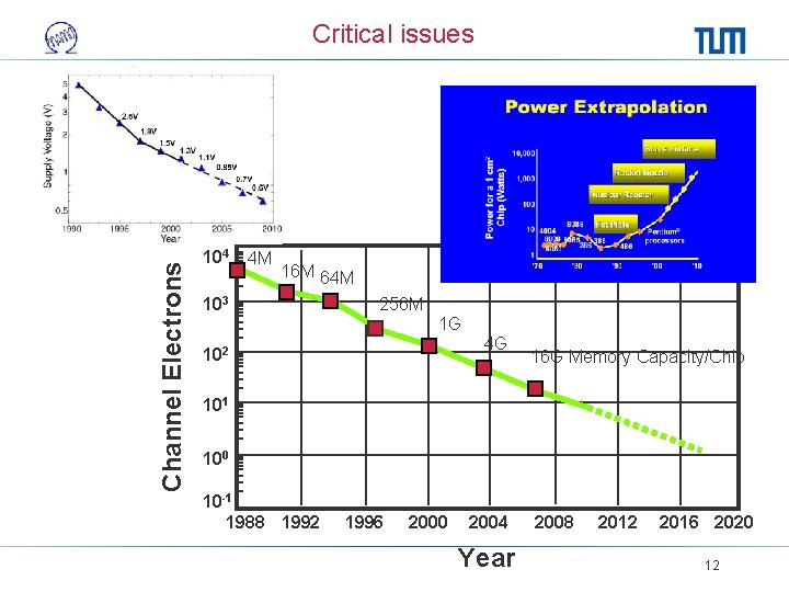
Channel Electrons Critical issues 104 4 M 16 M 64 M 103 256 M 1 G 4 G 102 16 G Memory Capacity/Chip 101 100 10 -1 1988 1992 1996 2000 2004 Year 2008 2012 2016 2020 12
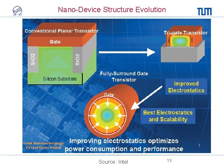
Nano-Device Structure Evolution Source: Intel 13
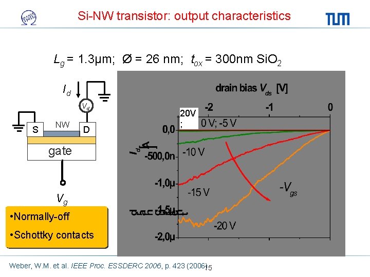
Si-NW transistor: output characteristics Lg = 1. 3µm; Ø = 26 nm; tox = 300 nm Si. O 2 Id Vd S NW D 20 V ; gate Vg • Normally-off • Schottky contacts Weber, W. M. et al. IEEE Proc. ESSDERC 2006, p. 423 (2006)15
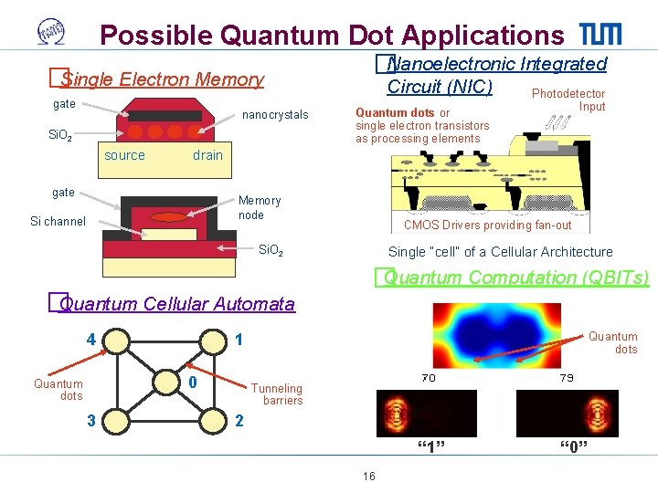
Possible Quantum Dot Applications Nanoelectronic Integrated � �Single Electron Memory Circuit (NIC) Photodetector gate nanocrystals Si. O 2 source drain gate Memory node Si channel CMOS Drivers providing fan-out Si. O 2 Quantum Cellular Automata � 4 3 Single “cell” of a Cellular Architecture Quantum Computation (QBITs) � Quantum dots 1 0 Quantum dots Input Quantum dots or single electron transistors as processing elements Tunneling barriers 2 “ 1” 16 “ 0”
Beyond Moore Beyond CMOS logic and memory device candidates: • Nanowire transistors • CNT transistors • Resonant tunneling devices • NEMS devices • Single electron transistors • Molecular devices • Spintronic devices All those candidates (some of which not yet demonstrated) still suffer from major reliability and stability problems 17
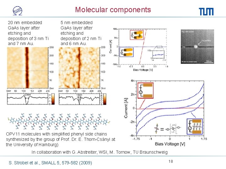
Molecular components 20 nm embedded Ga. As layer after etching and deposition of 3 nm Ti and 7 nm Au. 5 nm embedded Ga. As layer after etching and deposition of 2 nm Ti and 6 nm Au. OPV 11 molecules with simplified phenyl side chains synthesized by the group of Prof. Dr. E. Thorn-Csányi at the University of Hamburg) In collaboration with G. Abstreiter, WSI, M. Tornow, TU Braunschweig S. Strobel et al. , SMALL 5, 579 -582 (2009) 18
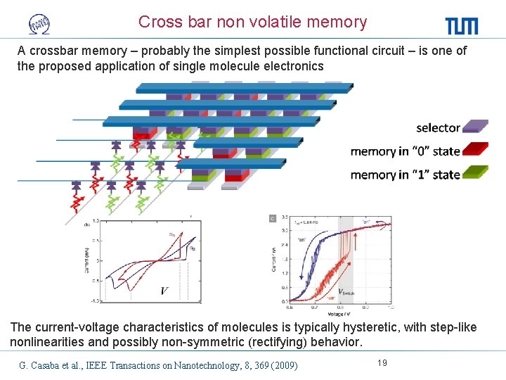
Cross bar non volatile memory A crossbar memory – probably the simplest possible functional circuit – is one of the proposed application of single molecule electronics The current-voltage characteristics of molecules is typically hysteretic, with step-like nonlinearities and possibly non-symmetric (rectifying) behavior. G. Casaba et al. , IEEE Transactions on Nanotechnology, 8, 369 (2009) 19
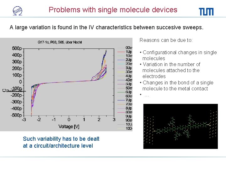
Problems with single molecule devices A large variation is found in the IV characteristics between succesive sweeps. Reasons can be due to: • Configurational changes in single molecules • Variation in the number of molecules attached to the electrodes • Changes in the bond of a single molecule to the metal contact • … Such variability has to be dealt at a circuit/architecture level
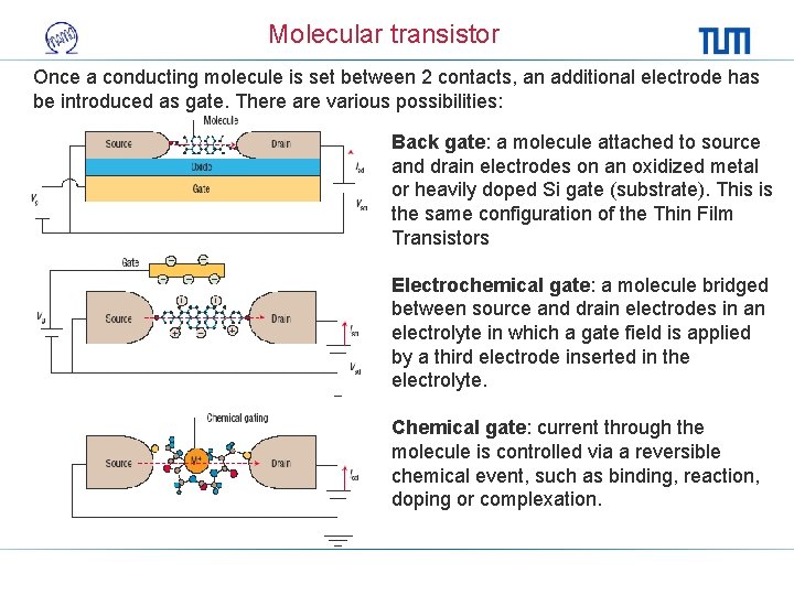
Molecular transistor Once a conducting molecule is set between 2 contacts, an additional electrode has be introduced as gate. There are various possibilities: Back gate: a molecule attached to source and drain electrodes on an oxidized metal or heavily doped Si gate (substrate). This is the same configuration of the Thin Film Transistors Electrochemical gate: a molecule bridged between source and drain electrodes in an electrolyte in which a gate field is applied by a third electrode inserted in the electrolyte. Chemical gate: current through the molecule is controlled via a reversible chemical event, such as binding, reaction, doping or complexation.
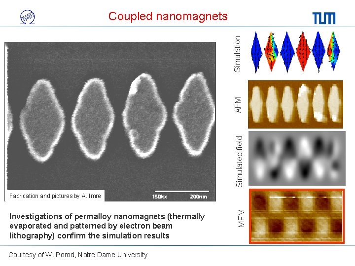
Simulated field AFM Simulation Coupled nanomagnets Investigations of permalloy nanomagnets (thermally evaporated and patterned by electron beam lithography) confirm the simulation results Courtesy of W. Porod, Notre Dame University MFM Fabrication and pictures by A. Imre
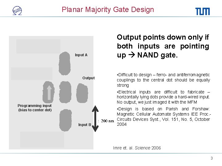
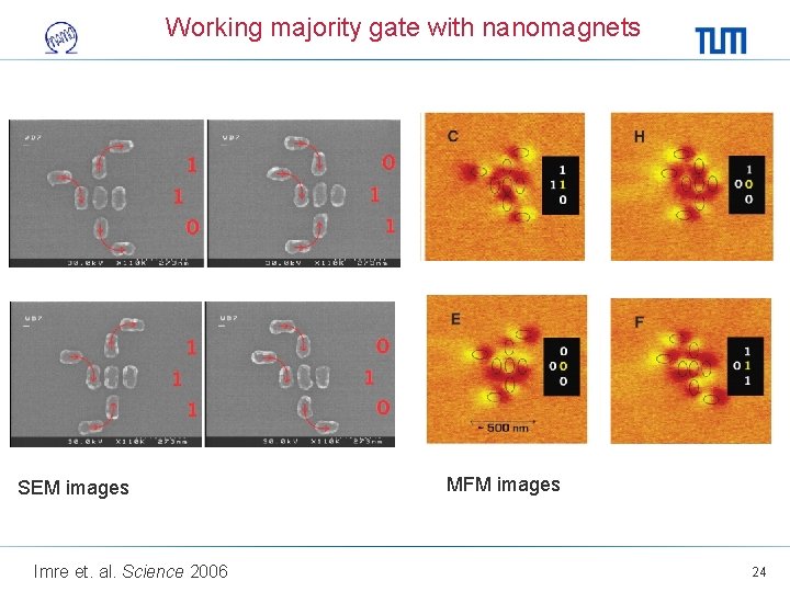
Planar Majority Gate Design Input A Output points down only if both inputs are pointing up NAND gate. • Difficult to design – ferro- and antiferromagnetic couplings to the central dot should be equally strong • Electrical inputs are difficult to fabricate – horizontally lying dots provide a hard-wired input. No output, we just imaged it with the MFM Programming input (bias to center dot) Input B • Design is based on Parish and Forshaw: Magnetic Cellular Automate Systems IEE Proc. Circuits Devices Syst. , Vol. 151, No. 5, October 2004 Imre et. al. Science 2006 3
Working majority gate with nanomagnets SEM images Imre et. al. Science 2006 MFM images 24
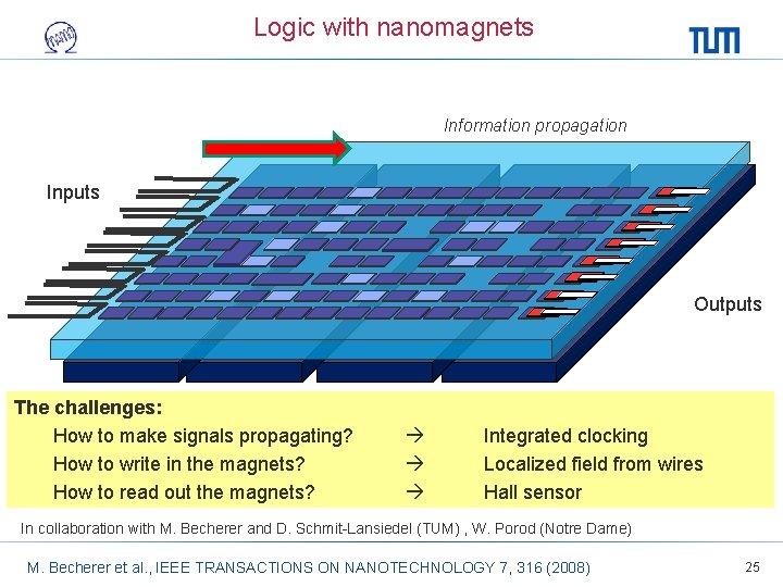
Logic with nanomagnets Information propagation Inputs Outputs The challenges: How to make signals propagating? How to write in the magnets? How to read out the magnets? Integrated clocking Localized field from wires Hall sensor In collaboration with M. Becherer and D. Schmit-Lansiedel (TUM) , W. Porod (Notre Dame) M. Becherer et al. , IEEE TRANSACTIONS ON NANOTECHNOLOGY 7, 316 (2008) 25
More than Moore Interfacing to the real world If the interaction is based on a non-electrical phenomenon, then specific transducers are required. Sensors, actuators, displays, imagers, fluidic or biointerfaces (DNA, Protein, Lab-On-Chip, Neuron interfaces, etc. ) are in this category Enhancing electronics with non-pure electrical devices New devices can be used in RF or analog circuits and signal processing. Thanks to electrical characteristics or transfer functions that are unachievable by regular MOS circuits, it is possible to reach better system performances. RF MEMS electro-acoustic high Q resonators are a good example of this category. Embedding power sources with the electronics: Several new applications will require on-chip or in-package micro power sources (autonomous sensors or circuits with permanent active security monitoring for instance). Energy scavenging micro-sources or micro-batteries are examples of this category. 26
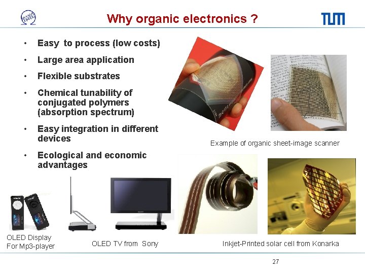
Why organic electronics ? • Easy to process (low costs) • Large area application • Flexible substrates • Chemical tunability of conjugated polymers (absorption spectrum) • Easy integration in different devices • Example of organic sheet-image scanner Ecological and economic advantages OLED Display For Mp 3 -player OLED TV from Sony Inkjet-Printed solar cell from Konarka 27
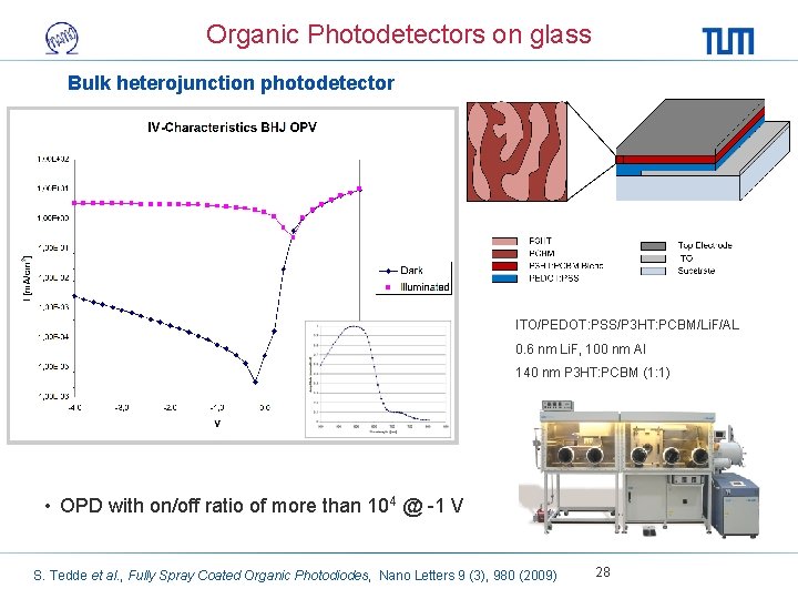
Organic Photodetectors on glass Bulk heterojunction photodetector ITO/PEDOT: PSS/P 3 HT: PCBM/Li. F/AL 0. 6 nm Li. F, 100 nm Al 140 nm P 3 HT: PCBM (1: 1) • OPD with on/off ratio of more than 104 @ -1 V S. Tedde et al. , Fully Spray Coated Organic Photodiodes, Nano Letters 9 (3), 980 (2009) 28
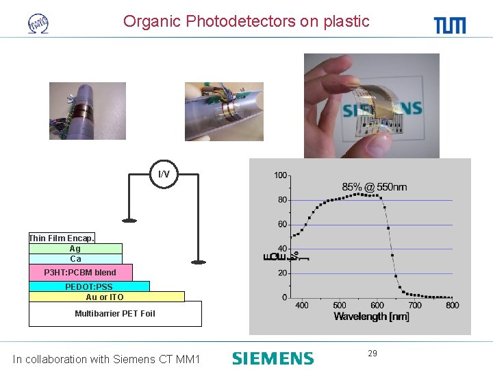
Organic Photodetectors on plastic I/V Thin Film Encap. Ag Ca P 3 HT: PCBM blend PEDOT: PSS Au or ITO Multibarrier PET Foil In collaboration with Siemens CT MM 1 29
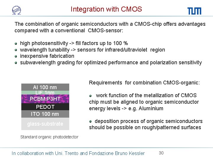
Integration with CMOS The combination of organic semiconductors with a CMOS-chip offers advantages compared with a conventional CMOS-sensor: high photosensitivity -> fill factors up to 100 % wavelength tunability -> sensors for infrared/ultraviolet region inexpensive fabrication subwavelength grading for optimized performance and polarization sensitivity Al 100 nm Li. F 1 nm PCBM: P 3 HT PEDOT ITO 100 nm glass-substrate Requirements for combination CMOS-organic: work function of the metallization of CMOS chip must be aligned to organic semiconductor energy levels -> e. g. Aluminium deposition process of organic semiconductors should be possible on rough/patterned surfaces Standard organic photodetector In collaboration with Uni. Trento and Fondazione Bruno Kessler 30
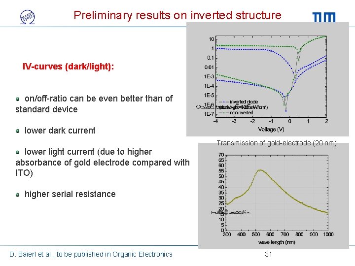
Preliminary results on inverted structure IV-curves (dark/light): on/off-ratio can be even better than of standard device lower dark current lower light current (due to higher absorbance of gold electrode compared with ITO) Transmission of gold-electrode (20 nm) higher serial resistance D. Baierl et al. , to be published in Organic Electronics 31
Conclusions q Nanotechnology provides a variety of interesting and promising nanostructures q Integration with CMOS will be the first step in the profitable use of nanostructures, once process compatibility is proven q Critical issues such as reliability, stability and lifetime are going to become routine and will have to be addressed at a circuit/architecture level q Novel circuits and architectures are going to be needed for a full exploitation of nanocomponents 32
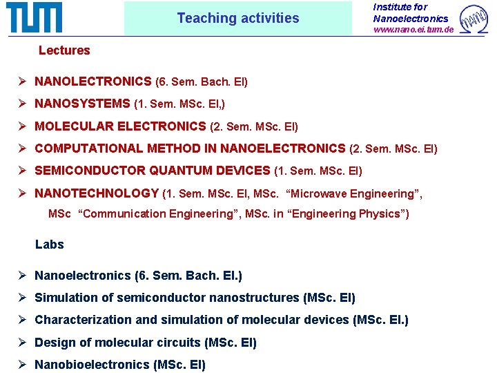
Teaching activities Institute for Nanoelectronics www. nano. ei. tum. de Lectures Ø NANOLECTRONICS (6. Sem. Bach. EI) Ø NANOSYSTEMS (1. Sem. MSc. EI, ) Ø MOLECULAR ELECTRONICS (2. Sem. MSc. EI) Ø COMPUTATIONAL METHOD IN NANOELECTRONICS (2. Sem. MSc. EI) Ø SEMICONDUCTOR QUANTUM DEVICES (1. Sem. MSc. EI) Ø NANOTECHNOLOGY (1. Sem. MSc. EI, MSc. “Microwave Engineering”, MSc “Communication Engineering”, MSc. in “Engineering Physics”) Labs Ø Nanoelectronics (6. Sem. Bach. EI. ) Ø Simulation of semiconductor nanostructures (MSc. EI) Ø Characterization and simulation of molecular devices (MSc. EI. ) Ø Design of molecular circuits (MSc. EI) Ø Nanobioelectronics (MSc. EI)
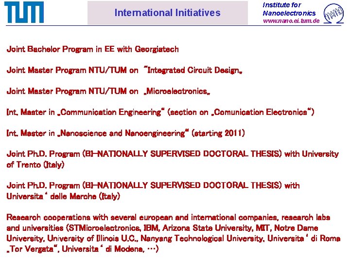
International Initiatives Institute for Nanoelectronics www. nano. ei. tum. de Joint Bachelor Program in EE with Georgiatech Joint Master Program NTU/TUM on "Integrated Circuit Design„ Joint Master Program NTU/TUM on „Microelectronics„ Int. Master in „Communication Engineering“ (section on „Comunication Electronics“) Int. Master in „Nanoscience and Nanoengineering“ (starting 2011) Joint Ph. D. Program (BI-NATIONALLY SUPERVISED DOCTORAL THESIS) with University of Trento (Italy) Joint Ph. D. Program (BI-NATIONALLY SUPERVISED DOCTORAL THESIS) with Universita‘ delle Marche (Italy) Research cooperations with several european and international companies, research labs and universities (STMicroelectronics, IBM, Arizona State University, MIT, Notre Dame University, University of Illinois U. C. , Nanyang Technological University, Universita‘ di Roma „Tor Vergata“, Universita‘ di Modena, …)
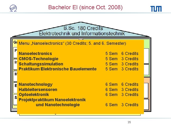
Bachelor EI (since Oct. 2008) Menu „Nanoelectronics“ (30 Credits; 5. and 6. Semester) Nanoelectronics CMOS-Technologie Schaltungssimulation Praktikum Elektronische Bauelemente 5 Sem 6 Credits 3 Credits Nanotechnology Halbleitersensoren Optoelektronik Projektpraktikum Nanoelektronik und Nanotechnologie 6 Sem 6 Credits 6 Sem 3 Credits 35
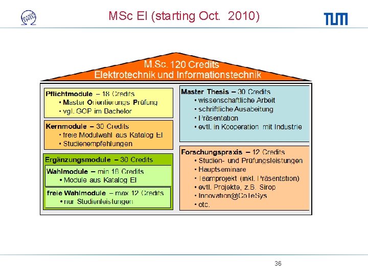
MSc EI (starting Oct. 2010) 36
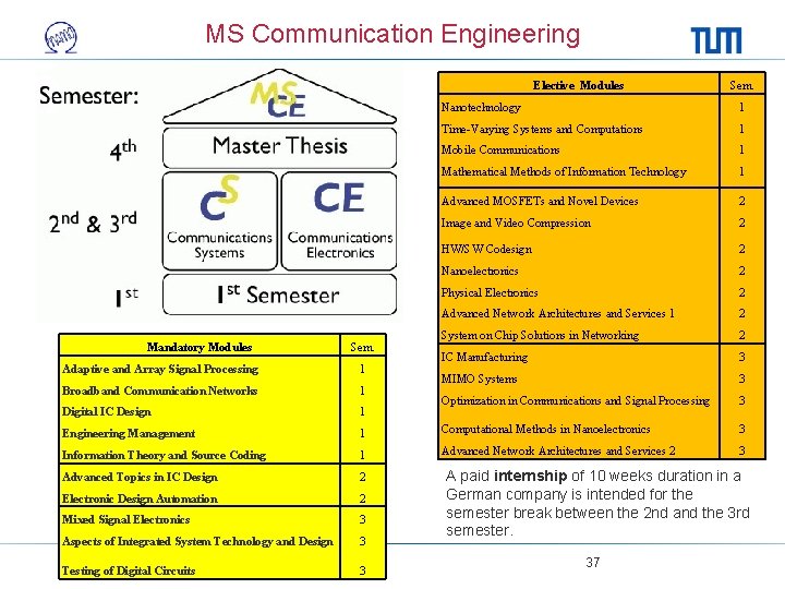
MS Communication Engineering Elective Modules Mandatory Modules Sem. Nanotechnology 1 Time-Varying Systems and Computations 1 Mobile Communications 1 Mathematical Methods of Information Technology 1 Advanced MOSFETs and Novel Devices 2 Image and Video Compression 2 HW/SW Codesign 2 Nanoelectronics 2 Physical Electronics 2 Advanced Network Architectures and Services 1 2 System on Chip Solutions in Networking 2 IC Manufacturing 3 MIMO Systems 3 Optimization in Communications and Signal Processing 3 Adaptive and Array Signal Processing 1 Broadband Communication Networks 1 Digital IC Design 1 Engineering Management 1 Computational Methods in Nanoelectronics 3 Information Theory and Source Coding 1 Advanced Network Architectures and Services 2 3 Advanced Topics in IC Design 2 Electronic Design Automation 2 Mixed Signal Electronics 3 Aspects of Integrated System Technology and Design 3 Testing of Digital Circuits 3 A paid internship of 10 weeks duration in a German company is intended for the semester break between the 2 nd and the 3 rd semester. 37
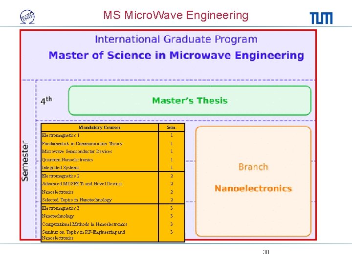
MS Micro. Wave Engineering Mandatory Courses Sem. Electromagnetics 1 1 Fundamentals in Communication Theory 1 Microwave Semiconductor Devices 1 Quantum Nanoelectronics 1 Integrated Systems 1 Electromagnetics 2 2 Advanced MOSFETs and Novel Devices 2 Nanoelectronics 2 Selected Topics in Nanotechnology 2 Electromagnetics 3 3 Nanotechnology 3 Computational Methods in Nanoelectronics 3 Seminar on Topics in RF-Engineering and Nanoelectronics 3 38
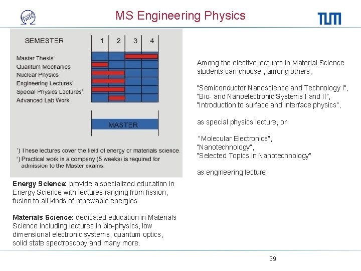
MS Engineering Physics Among the elective lectures in Material Science students can choose , among others, “Semiconductor Nanoscience and Technology I”, “Bio- and Nanoelectronic Systems I and II”, “Introduction to surface and interface physics”, as special physics lecture, or “Molecular Electronics”, “Nanotechnology”, “Selected Topics in Nanotechnology” as engineering lecture Energy Science: provide a specialized education in Energy Science with lectures ranging from fission, fusion to all kinds of renewable energies. Materials Science: dedicated education in Materials Science including lectures in bio-physics, low dimensional electronic systems, quantum optics, solid state spectroscopy and many more. 39
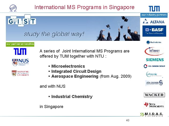
International MS Programs in Singapore A series of Joint International MS Programs are offered by TUM together with NTU : § Microelectronics § Integrated Circuit Design § Aerospace Engineering (from Aug. 2009) and with NUS § Industrial Chemistry in Singapore 40
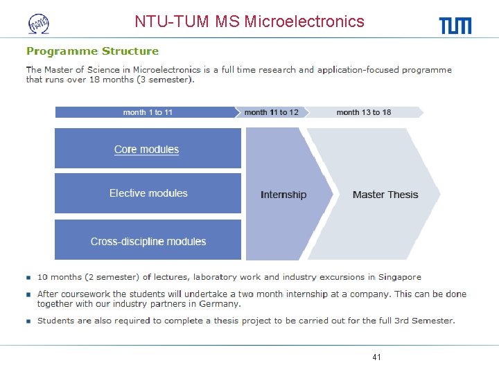
NTU-TUM MS Microelectronics 41
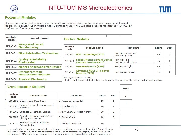
NTU-TUM MS Microelectronics 42
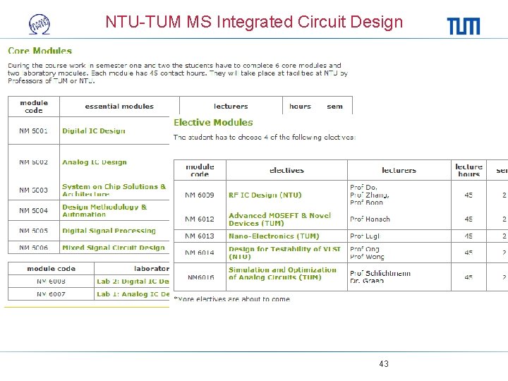
NTU-TUM MS Integrated Circuit Design 43
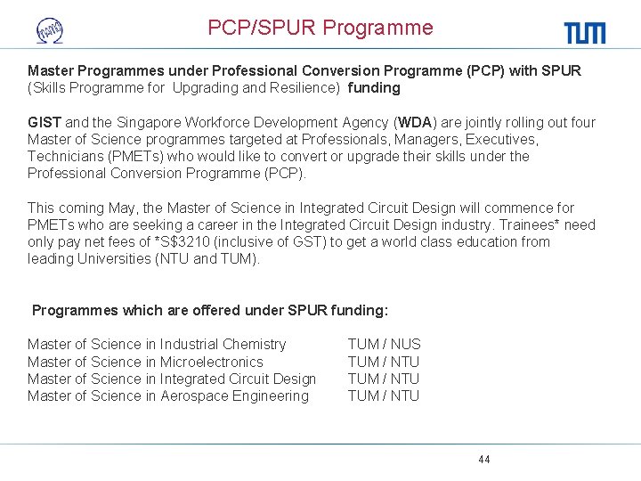
PCP/SPUR Programme Master Programmes under Professional Conversion Programme (PCP) with SPUR (Skills Programme for Upgrading and Resilience) funding GIST and the Singapore Workforce Development Agency (WDA) are jointly rolling out four Master of Science programmes targeted at Professionals, Managers, Executives, Technicians (PMETs) who would like to convert or upgrade their skills under the Professional Conversion Programme (PCP). This coming May, the Master of Science in Integrated Circuit Design will commence for PMETs who are seeking a career in the Integrated Circuit Design industry. Trainees* need only pay net fees of *S$3210 (inclusive of GST) to get a world class education from leading Universities (NTU and TUM). Programmes which are offered under SPUR funding: Master of Science in Industrial Chemistry Master of Science in Microelectronics Master of Science in Integrated Circuit Design Master of Science in Aerospace Engineering TUM / NUS TUM / NTU 44
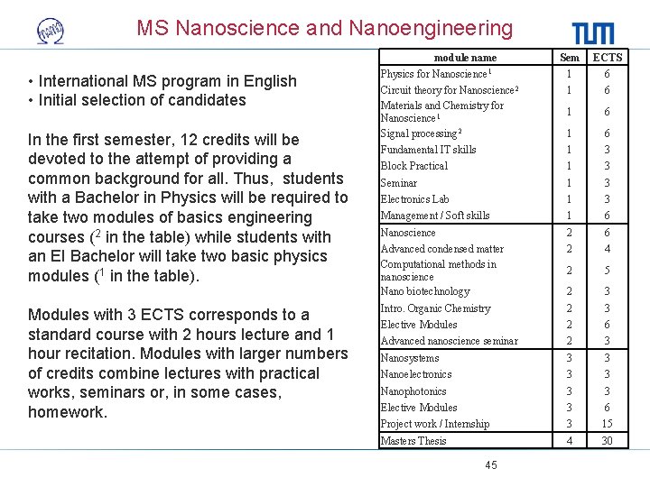
MS Nanoscience and Nanoengineering module name • International MS program in English • Initial selection of candidates In the first semester, 12 credits will be devoted to the attempt of providing a common background for all. Thus, students with a Bachelor in Physics will be required to take two modules of basics engineering courses (2 in the table) while students with an EI Bachelor will take two basic physics modules (1 in the table). Modules with 3 ECTS corresponds to a standard course with 2 hours lecture and 1 hour recitation. Modules with larger numbers of credits combine lectures with practical works, seminars or, in some cases, homework. Sem ECTS Physics for Nanoscience 1 1 6 Circuit theory for Nanoscience 2 Materials and Chemistry for Nanoscience 1 Signal processing 2 1 6 1 6 Fundamental IT skills 1 3 Block Practical 1 3 Seminar 1 3 Electronics Lab 1 3 Management / Soft skills 1 6 Nanoscience 2 6 Advanced condensed matter Computational methods in nanoscience Nano biotechnology 2 4 2 5 2 3 Intro. Organic Chemistry 2 3 Elective Modules 2 6 Advanced nanoscience seminar 2 3 Nanosystems 3 3 Nanoelectronics 3 3 Nanophotonics 3 3 Elective Modules 3 6 Project work / Internship 3 15 Masters Thesis 4 30 45
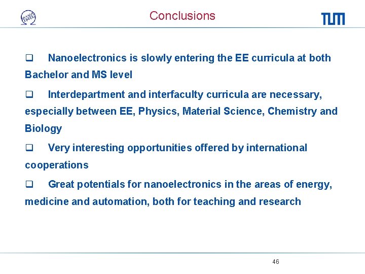
Conclusions q Nanoelectronics is slowly entering the EE curricula at both Bachelor and MS level q Interdepartment and interfaculty curricula are necessary, especially between EE, Physics, Material Science, Chemistry and Biology q Very interesting opportunities offered by international cooperations q Great potentials for nanoelectronics in the areas of energy, medicine and automation, both for teaching and research 46
Thanks for your attention! 47
Acknowledgments Institute for Nanoelectronics U Tor Vergata MDM nan o 48