Microwave Devices Microwave Passive Devices I 7 2008

 Zo=f(w/h) h w (( (( GND (( (( w s GND")
 Metal h~100 µm 5 -10 µm Au plating GND")
 ( ( ( signal GND ( E GND - frequency에 따른")
 GND a h b co bottom ground - 측정시 발생 (unwanted)")
, tanδ=0. 002, s=50 m, w=75")
 maximum deflection at the center Dmax L")
 • S. N. U. EE Microwave Devices")


 Ksurface wave")
 Surface wave mode substrate ( r) Parallel-plate mode GND")
 * conductor-backed dielectric slab h - TM 0 mode")
 Ref. ) Sung-Jin Kim, et")
 Ref. ) Sung-Jin Kim, et")


 – U. Michigan *")

 - low loss")
 (Ref. : H.")
 Sung-Jin Kim, et al,")
 A. Tessmann, et al, IEEE MTT Symp.")
 A. Tessmann, et al, IEEE MTT Symp. ,")
 Ref. ) A. Margomenos, et al,")
 Ref. ) A. Margomenos, et al,")

 J. H. Wu, et al, IEEE")
 Ref. ) L. Katehi,")

 Nanophotonic waveguides -")
 Wave-blocking structures in ground")
 (CPW 응용) (Microstrip 응용)")


 H. -T. Kim, et al, IEEE Trans. MTT, p.")

")
- Slides: 41
Microwave Devices - Microwave Passive Devices I – 7 2008 / 1 학기 서광석 • S. N. U. EE Microwave Devices 2008
Coplanar Waveguide (1) Zo=f(w/h) h w (( (( GND (( (( w s GND Zo=g(w/s) GND <Microstrip> CPW의 장점 <CPW> 1. No wafer thinning 2. Easy grounding 3. Small frequency dispersion CPW의 단점 1. 같은 loss와 Zo의 경우 microstrip에 비해 넓은 면적 차지 (GND plane으로 인해) 2. thick substrate의 사용으로 인해 열 방출이 어려움. • S. N. U. EE Microwave Devices 2008
Microstrip의 Via Connection (via-hole process) Metal h~100 µm 5 -10 µm Au plating GND - Parasitic ground inductance : ~ 50 -60 p. H for 100 m diameter via Wet etching Photoresist Dry etching (ion-milling) * h를 작게 해주면 (25~50 µm) inductance 감소 : process 어려움. 60° Dry etching (reactive ion-milling) • S. N. U. EE 60° Thin Au sputtering (4000Å) Thick Au plating Microwave Devices 2008
Coplanar Waveguide (2) ( ( ( signal GND ( E GND - frequency에 따른 effective 의 변화가 작음 thick substrate ( r ) (millimeter-wave에 적합) - surface mode의 leakage에 의해 Surface mode로 leakage ( ( ( ( ( - 없을 경우: slot-line-mode 발생 ( (( ( signal <Finite Ground CPW> • S. N. U. EE - Equipotential을 위한 air bridge connection이 필요 ( GND ( problem frequency dispersion - GND loss로 인해 전체 loss 증가 - signal line/GND line width 를 증가시켜 loss 감소 가능 Microwave Devices 2008
Coplanar Waveguide (3) GND a h b co bottom ground - 측정시 발생 (unwanted) h/b > 3 일 때 Zo = function of (a/b) co/b > 3 일 때 Zo = function of (a/b) For Ga. As substrate, Zo=50 a/b=0. 35 a에 의해 conductor loss 결정 - MMIC의 경우 a ~ (25 -50) µm - digital IC의 경우 a ~ 1 µm bended CPW 구조 Air-bridge connection to avoid higher mode generation • S. N. U. EE Microwave Devices 2008
Full-Wave Analysis of CPW Structures =12. 9 (Ga. As), tanδ=0. 002, s=50 m, w=75 m Even Mode (CPW Mode) Odd Mode (Slot-line Mode) Ref. : I. Wolff, “Coplanar Microwave Integrated Circuits, ” p. 31, Wiley, 2006 • S. N. U. EE Microwave Devices 2008
Air-Bridge Technology for Air. Gap Formation (1) maximum deflection at the center Dmax L 4/EWT 2 Air-Bridge Process • S. N. U. EE L : the span E : the Young’s modulus W : the width T : the thickness Microwave Devices 2008
Air-Bridge Technology for Air. Gap Formation (2) • S. N. U. EE Microwave Devices 2008
Suppression of the Parasitic Modes Using MCM-D Technology - Instead of air bridge, tunnel is formed by using BCB thin film process. Ref. : Ezzeldin A. Soliman, IEEE T. MTT, p. 2426, 1998 • S. N. U. EE Microwave Devices 2008
Conductor-Backed CPW Structure Ref. : I. Wolff, “Coplanar Microwave Integrated Circuits, ” p. 78, Wiley, 2006 • S. N. U. EE Microwave Devices 2008
Trenched CPW for Si MMIC Applications - Si Resistivity : 10 -20 -cm - CF 4 plasma etch : 1. 5 m/hr (Ref. : Z. R. Hu et al, p. 735, 1997 IEEE MTT-S Digest) • S. N. U. EE Microwave Devices 2008
Surface Waves in CPW Dielectric Waveguide 1 d > c 일 때 total reflection. 2 - 높은 주파수에서 유용함. ( >60 GHz ) 1 decay coeff. w - optical fiber (d~10 m for ~1. 5 m) Surface Waves in CPW (1) (3) (2) (4) GND (Conductor-Backed CPW) • S. N. U. EE Microwave Devices 2008
Conductor-Backed CPW 구조의 Leakage Kcpw z 일 때 strong interaction (mode-conversion leakage) Ksurface wave surface mode로 conversion – loss 발생 fundamental TEM mode로의 coupling에 의한 attenuation (Ref : M. Riaziat et al, IEEE T. MTT, pp. 245 -251, 1990) * (Ksurface wave)TEM > Kcpw 를 만족하여 leak가 2 b=h/4 < 1/20 d 일 때 발생하지만 (Ksurface wave)z ~ (Kcpw)z 가 attenuation < 0. 17 d. B/ g 안 일어나므로 small leakage 발생 • S. N. U. EE Microwave Devices 2008
CPW 구조의 Leaky Modes (1) Surface wave mode substrate ( r) Parallel-plate mode GND substrate ( r) - TEM mode from DC - higher order modes TE, TM • S. N. U. EE Microwave Devices 2008
CPW 구조의 Leaky Modes (2) * conductor-backed dielectric slab h - TM 0 mode : lowest mode - 2 h ~ 0. 35 g 일 때 v. P, CPW ~ v. P, SW h < 0. 12 g 일 때 small leak substrate * metal이 없는 dielectric slab h substrate - TE 0 mode : lowest mode h < 0. 1 g 일 때 small leak • S. N. U. EE Microwave Devices 2008
Leakage Resonance in CPW MMIC Packages ( I ) Ref. ) Sung-Jin Kim, et al, IEEE Tran. MTT, p. 2664, Dec. 2000 • S. N. U. EE Microwave Devices 2008
Leakage Resonance in CPW MMIC Packages ( II ) Ref. ) Sung-Jin Kim, et al, IEEE Tran. MTT, p. 2664, Dec. 2000 • S. N. U. EE Microwave Devices 2008
Nonleaky CBCPW Structure r 1 h 1 r 2 h 2 ** GND far field에서 canceling에 의해 small radiation slot-line 혹은 -strip으로 안테나 구현 • S. N. U. EE Microwave Devices 2008
Small Loss CPW Structures – Finite ground CPW D Wg GND Kcpw K surface wave Finite Ground CPW (FGCPW) h Wg ground (Wg)optimum D (Ref. : J. Papapolymerou et al, IEEE T. MTT, p. 614, 1999) (h=500 m, w=50 m, s=45 m) total line width=460 m higher mode cutoff frequency = 180 GHz * 94 GHz In. P HEMT Power Amp MMIC - Po, max=18. 6 d. Bm (HRL) (Ref, : p. 1212, JSSC 1999) • S. N. U. EE ~ 0. 2 d. B/ g ( g = 1 mm at 100 GHz) Microwave Devices 2008
FGCPW Structures – Equations for Attenuation (FGCPW : B=4 S) – U. Michigan * HRL used B=2 3 S. Ref. : G. E. Ponchak et al, p. 241, IEEE T. MTT, 1999. • S. N. U. EE Microwave Devices 2008
Loss Characteristics of CPW Lines on Si Substrate - commercial CMOS foundary - Zo=50 - 1 cm substrate - ground to ground spacing=50 m • S. N. U. EE Microwave Devices 2008
Low-Loss CPW Lines on Surface Stabilized High-Resistivity Si ( I ) - low loss - bias dependent한 특성 - low loss - unpassivated surface 존재 • S. N. U. EE - oxide charge에 의한 surface charge 유도로 인해 high loss - low loss (poly에 의한 charge trapping) - passivated surface Microwave Devices 2008
Low-Loss CPW Lines on Surface Stabilized High-Resistivity Si ( II ) (Ref. : H. S. Gamble, IEEE Microwave and Guided Wave Letters, p. 395, 1999) 그림. Measured microwave losses (a) directly on HRS substrate (b) on oxide passivated substrate (c) on patterned oxide (d) on passivated, polysilicon stabilized HRS substrate. * 1016 cm-2 proton implanted conventional Si substrate 106 cm, 6. 3 d. B/cm loss at 20 GHz • S. N. U. EE Microwave Devices 2008
Suppression of Leakage Resonance with Doped Si Substrate Ref. ) Sung-Jin Kim, et al, IEEE Tran. MTT, p. 2664, Dec. 2000 • S. N. U. EE Microwave Devices 2008
W-band Amplifier on Different Carriers Ref. ) A. Tessmann, et al, IEEE MTT Symp. , p. 543, 2001 • S. N. U. EE Microwave Devices 2008
Flip-Chip Mounted W-band Amplifier Ref. ) A. Tessmann, et al, IEEE MTT Symp. , p. 543, 2001 Port-to-Port Isolation without Chip Carrier • S. N. U. EE Microwave Devices 2008
Isolation in 3 -D ICs ( I ) Ref. ) A. Margomenos, et al, IEEE Trans. MTT, p. 25, Jan. 2003 • S. N. U. EE Microwave Devices 2008
Isolation in 3 -D ICs ( II ) Ref. ) A. Margomenos, et al, IEEE Trans. MTT, p. 25, Jan. 2003 • S. N. U. EE Microwave Devices 2008
Isolation in Si MMIC Module Isolation Properties at 1 GHz with Metal Plate Ref. ) T. Nishino, et al, IEEE MTT Symp. , p. 1385, 2002 • S. N. U. EE Microwave Devices 2008
Improved Isolation Structure with Faraday Cage Ref. ) J. H. Wu, et al, IEEE MWCL, p. 410, 2001 • S. N. U. EE Microwave Devices 2008
SAWLIT for Heterogeneous Integration Silicon-based, self-aligned wafer-level integration technology (SAWLIT) Ref. ) L. Katehi, et al. , “Heterogeneous wafer-scale circuits architectures, ” IEEE Microwave Mag. p. 52, 2007 • S. N. U. EE Microwave Devices 2008
Improved Isolation with Faraday cage processed with SAWLIT A two-port structure with the separation distance of 100μm < processed with SAWLIT & Faraday cage isolation > Ref. ) H. Sharifi, et al. , p. 147, Si. RF 2008 • S. N. U. EE Microwave Devices 2008
Photonic Crystals Periodic Electromagnetic Media (Ref. : http: //ab-initio. mit. edu/photons/tutorial) Nanophotonic waveguides - Smaller waveguides - Sharper bends • S. N. U. EE Microwave Devices 2008
Small Loss CPW Structures – Photonic Bandgap Structure의 응용 (1) Wave-blocking structures in ground planes GND Ref) A unipolar photonic-bandgap structure and its applications to microwave circuits IEEE T. MTT, Aug. 1999. p. 1509~1514 GND Photonic-bandgap structure * Superlattice A B A B A B A mini-band • S. N. U. EE Microwave Devices 2008
Small Loss CPW Structures – Photonic Bandgap Structure의 응용 (2) (CPW 응용) (Microstrip 응용) * ka= 에서 stop band • S. N. U. EE Microwave Devices 2008
Microstrip with Periodically Perforated Ground Metal λ/4 transformer with Z 0=14. 1Ω for impedance matching Microstrip Line f=7 GHz W λg /4 microstrip 550 m 3. 3 mm PPGM 20 m 0. 425 mm Small Z 0 Microstrip Transmission Line with Periodically Perforated Ground Metals (PPGM) • S. N. U. EE Ref. : Y. Yun, et al. , p. 3805, IEEE Trans. MTT, 2006 Microwave Devices 2008
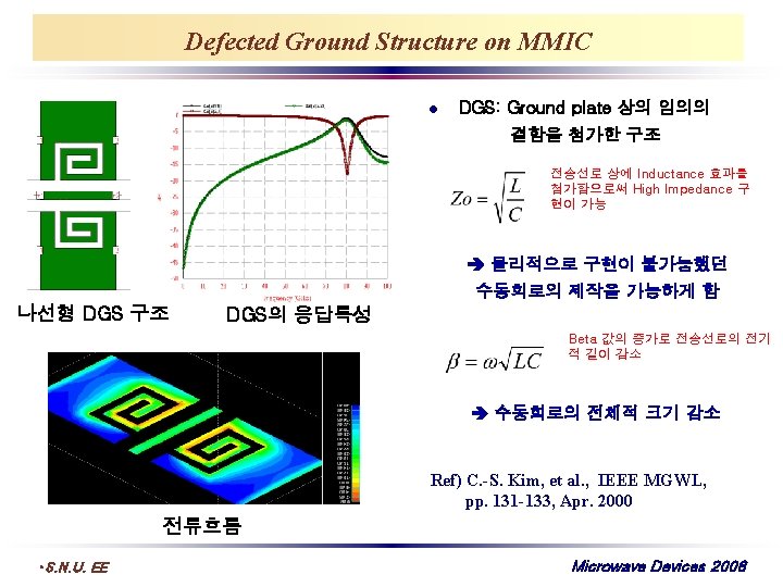
10 d. B Coupler using DGS Structure Spiral-shaped DGS를 이용한 W-Band 10 d. B Coupler 1 st signal (through) 2 nd signal (coupled) DGS 부분 l DGS를 이용하여 약 150 에 이르는 high impedance 값을 얻음 l 이 결과를 이용해서 비대칭( 1: 9 ) 전력 분배 비를 가지는 Branch-line Coupler 를 설계 및 제작 • S. N. U. EE Microwave Devices 2008
Micromachined Overlay CPW Ref. ) H. -T. Kim, et al, IEEE Trans. MTT, p. 1634, 2001 • S. N. U. EE Microwave Devices 2008
3 -D MMIC Using Photosensitive BCB Film Advantages of Photosensitive BCB Film - Via holes and trenches are formed by lithography - O 2 dry etching for photoresist removal does not attack the BCB film. - Lower moisture absorption offers short cure time. • S. N. U. EE Microwave Devices 2008
3 -D Low Loss CPW Lines Elevated CPW for high Z 0 Ref. ) V. T. Vo, et al, IEEE Trans. MTT, p. 2864, 2006 • S. N. U. EE V-shaped CPW for low Z 0 Microwave Devices 2008