Microwave Devices Microwave Passive Devices I 4 2008
![Future Directions of LTCC Technology Parameter 1998 2003 2009 Min. via size [μm] 250 Future Directions of LTCC Technology Parameter 1998 2003 2009 Min. via size [μm] 250](https://slidetodoc.com/presentation_image_h2/0b4b280e62409c0847299affccbf09f1/image-26.jpg)
- Slides: 32

Microwave Devices - Microwave Passive Devices I - 4 2008 / 1 학기 서광석 • S. N. U. EE Microwave Devices 2008

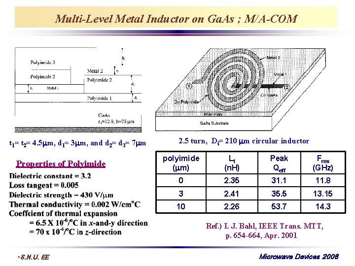
Multi-Level Metal Inductor on Ga. As ; M/A-COM t 1= t 2= 4. 5 m, d 1= 3 m, and d 2= d 3= 7 m Properties of Polyimide 2. 5 turn, Di= 210 m circular inductor polyimide ( m) Lt (n. H) Peak Qeff Fres (GHz) 0 2. 35 31. 1 11. 8 3 2. 41 35. 5 13. 15 10 2. 26 53. 7 14. 3 Ref. ) I. J. Bahl, IEEE Trans. MTT, p. 654 -664, Apr. 2001 • S. N. U. EE Microwave Devices 2008

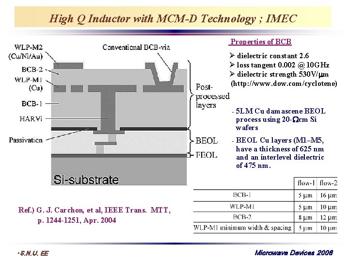
High Q Inductor with MCM-D Technology ; IMEC Properties of BCB Ø dielectric constant 2. 6 Ø loss tangent 0. 002 @ 10 GHz Ø dielectric strength 530 V/ m (http: //www. dow. com/cyclotene) - 5 LM Cu damascene BEOL process using 20 - cm Si wafers - BEOL Cu layers (M 1–M 5, have a thickness of 625 nm and an interlevel dielectric of 475 nm. Ref. ) G. J. Carchon, et al, IEEE Trans. MTT, p. 1244 -1251, Apr. 2004 • S. N. U. EE Microwave Devices 2008

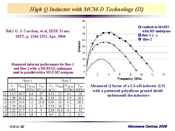
High Q Inductor with MCM-D Technology (II) Ref. ) G. J. Carchon, et al, IEEE Trans. MTT, p. 1244 -1251, Apr. 2004 realized in M 4/M 5 with M 3 underpass flow-1 (- -) flow-2 Measured inductor performance for flow-1 and flow-2 with a M 5 BEOL underpass used in parallel with a WLP-M 2 overpass Measured Q factor of a 2. 3 -n. H inductor (L 5) with a patterned polysilicon ground shield underneath the inductors • S. N. U. EE Microwave Devices 2008

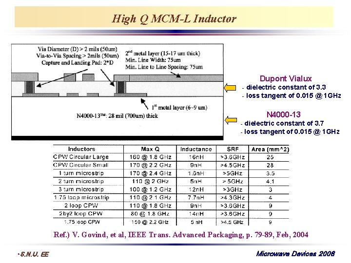
High Q MCM-L Inductor Dupont Vialux dielectric constant of 3. 3 - loss tangent of 0. 015 @ 1 GHz - N 4000 -13 dielectric constant of 3. 7 - loss tangent of 0. 015 @ 1 GHz - Ref. ) V. Govind, et al, IEEE Trans. Advanced Packaging, p. 79 -89, Feb, 2004 • S. N. U. EE Microwave Devices 2008

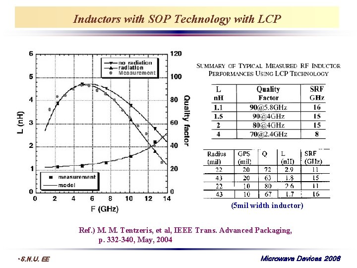
Inductors with SOP Technology with LCP (5 mil width inductor) Ref. ) M. M. Tentzeris, et al, IEEE Trans. Advanced Packaging, p. 332 -340, May, 2004 • S. N. U. EE Microwave Devices 2008

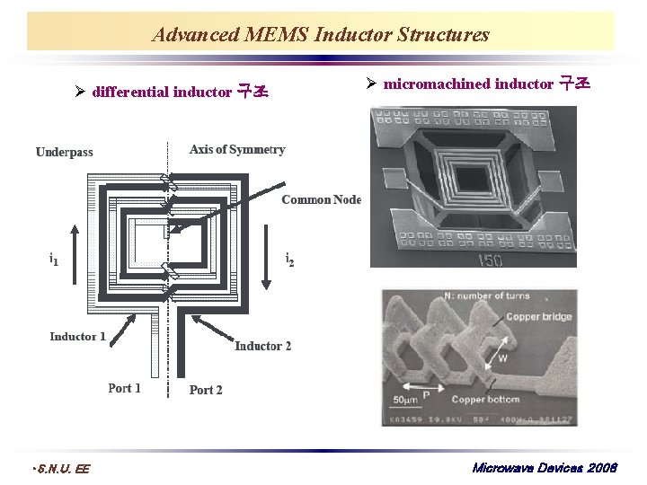
Advanced MEMS Inductor Structures Ø differential inductor 구조 • S. N. U. EE Ø micromachined inductor 구조 Microwave Devices 2008

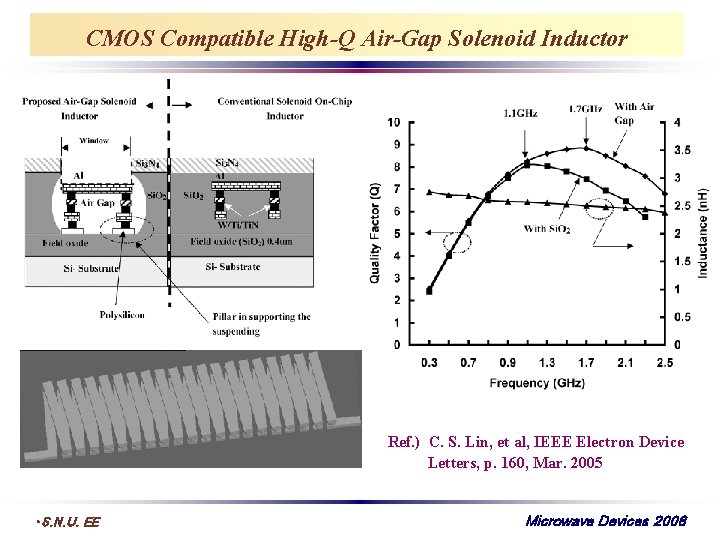
CMOS Compatible High-Q Air-Gap Solenoid Inductor Ref. ) C. S. Lin, et al, IEEE Electron Device Letters, p. 160, Mar. 2005 • S. N. U. EE Microwave Devices 2008

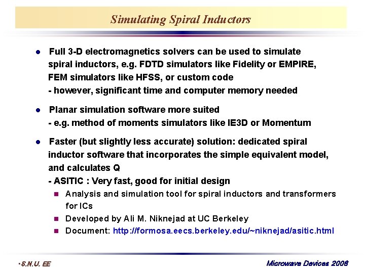
Simulating Spiral Inductors Full 3 -D electromagnetics solvers can be used to simulate spiral inductors, e. g. FDTD simulators like Fidelity or EMPIRE, FEM simulators like HFSS, or custom code - however, significant time and computer memory needed Planar simulation software more suited - e. g. method of moments simulators like IE 3 D or Momentum Faster (but slightly less accurate) solution: dedicated spiral inductor software that incorporates the simple equivalent model, and calculates Q - ASITIC : Very fast, good for initial design Analysis and simulation tool for spiral inductors and transformers for ICs n Developed by Ali M. Niknejad at UC Berkeley n Document: http: //formosa. eecs. berkeley. edu/~niknejad/asitic. html n • S. N. U. EE Microwave Devices 2008

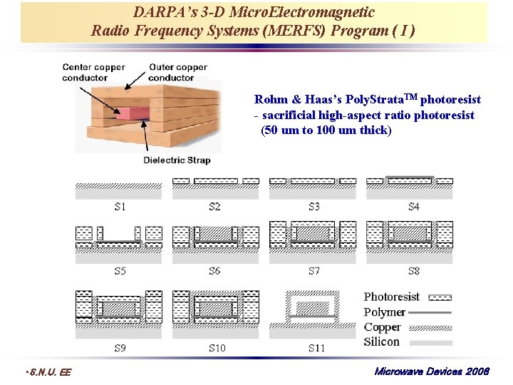
DARPA’s 3 -D Micro. Electromagnetic Radio Frequency Systems (MERFS) Program ( I ) Rohm & Haas’s Poly. Strata. TM photoresist - sacrificial high-aspect ratio photoresist (50 um to 100 um thick) • S. N. U. EE Microwave Devices 2008

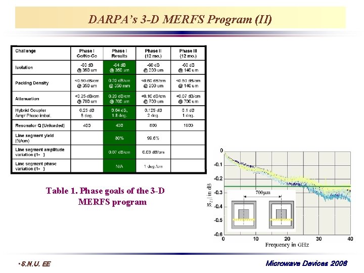
DARPA’s 3 -D MERFS Program (II) Table 1. Phase goals of the 3 -D MERFS program • S. N. U. EE Microwave Devices 2008

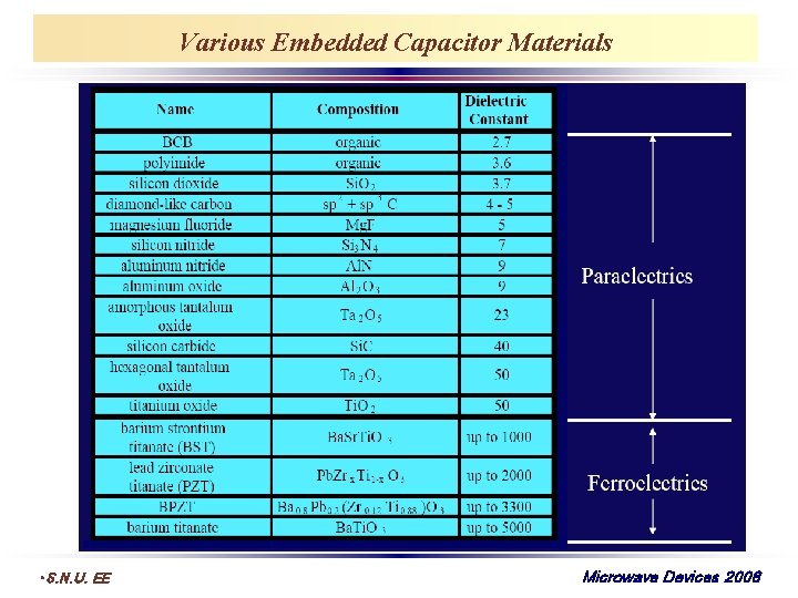
Various Embedded Capacitor Materials • S. N. U. EE Microwave Devices 2008

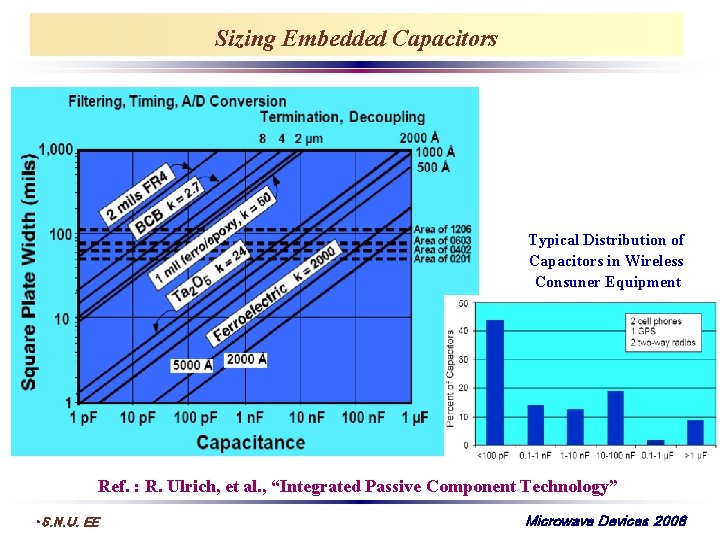
Sizing Embedded Capacitors Typical Distribution of Capacitors in Wireless Consuner Equipment Ref. : R. Ulrich, et al. , “Integrated Passive Component Technology” • S. N. U. EE Microwave Devices 2008

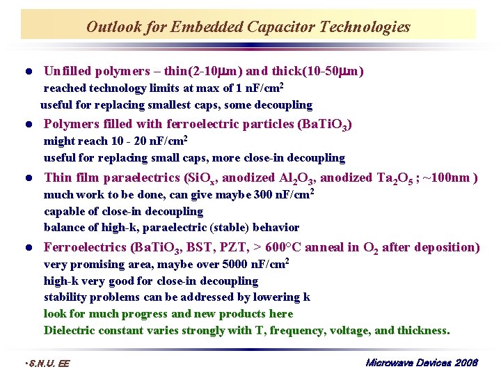
Outlook for Embedded Capacitor Technologies Unfilled polymers – thin(2 -10 m) and thick(10 -50 m) reached technology limits at max of 1 n. F/cm 2 useful for replacing smallest caps, some decoupling Polymers filled with ferroelectric particles (Ba. Ti. O 3) might reach 10 - 20 n. F/cm 2 useful for replacing small caps, more close-in decoupling Thin film paraelectrics (Si. Ox, anodized Al 2 O 3, anodized Ta 2 O 5 ; ~100 nm ) much work to be done, can give maybe 300 n. F/cm 2 capable of close-in decoupling balance of high-k, paraelectric (stable) behavior Ferroelectrics (Ba. Ti. O 3, BST, PZT, > 600°C anneal in O 2 after deposition) very promising area, maybe over 5000 n. F/cm 2 high-k very good for close-in decoupling stability problems can be addressed by lowering k look for much progress and new products here Dielectric constant varies strongly with T, frequency, voltage, and thickness. • S. N. U. EE Microwave Devices 2008

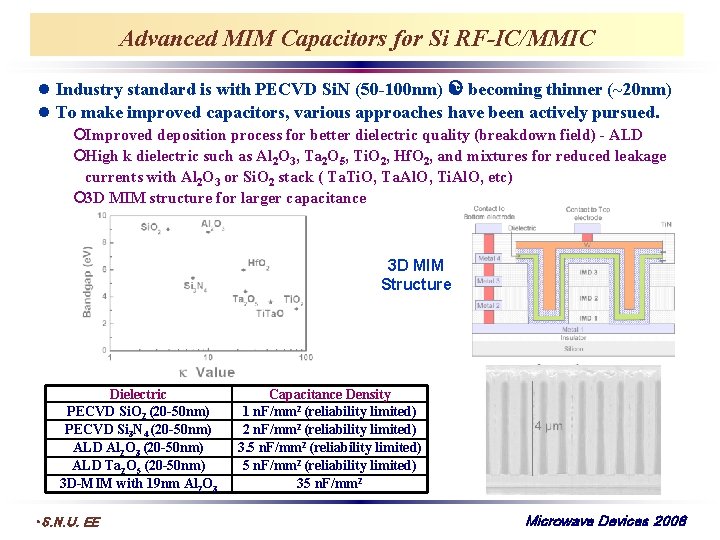
Advanced MIM Capacitors for Si RF-IC/MMIC Industry standard is with PECVD Si. N (50 -100 nm) becoming thinner (~20 nm) To make improved capacitors, various approaches have been actively pursued. ¡Improved deposition process for better dielectric quality (breakdown field) - ALD ¡High k dielectric such as Al 2 O 3, Ta 2 O 5, Ti. O 2, Hf. O 2, and mixtures for reduced leakage currents with Al 2 O 3 or Si. O 2 stack ( Ta. Ti. O, Ta. Al. O, Ti. Al. O, etc) ¡ 3 D MIM structure for larger capacitance 3 D MIM Structure Dielectric PECVD Si. O 2 (20 -50 nm) PECVD Si 3 N 4 (20 -50 nm) ALD Al 2 O 3 (20 -50 nm) ALD Ta 2 O 5 (20 -50 nm) 3 D-MIM with 19 nm Al 2 O 3 • S. N. U. EE Capacitance Density 1 n. F/mm 2 (reliability limited) 2 n. F/mm 2 (reliability limited) 3. 5 n. F/mm 2 (reliability limited) 35 n. F/mm 2 Microwave Devices 2008

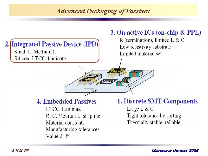
Advanced Packaging of Passives • S. N. U. EE Microwave Devices 2008

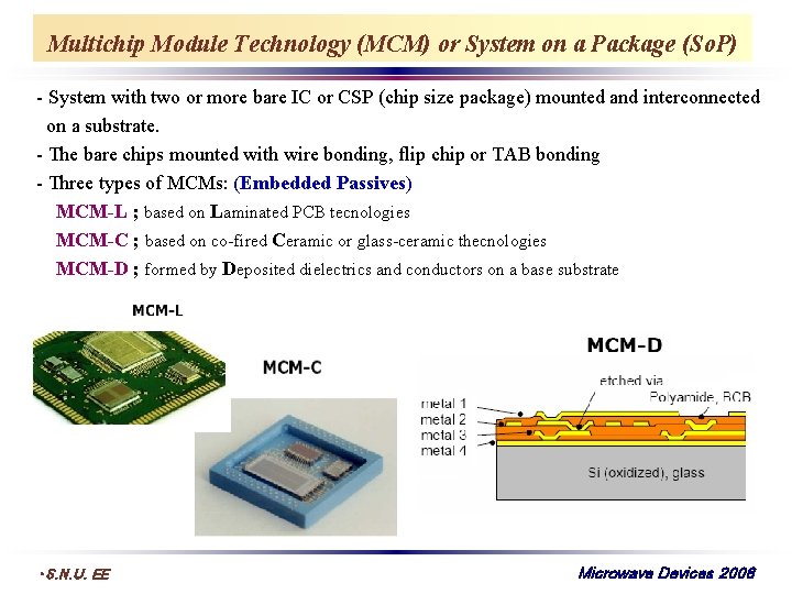
Multichip Module Technology (MCM) or System on a Package (So. P) - System with two or more bare IC or CSP (chip size package) mounted and interconnected on a substrate. - The bare chips mounted with wire bonding, flip chip or TAB bonding - Three types of MCMs: (Embedded Passives) MCM-L ; based on Laminated PCB tecnologies MCM-C ; based on co-fired Ceramic or glass-ceramic thecnologies MCM-D ; formed by Deposited dielectrics and conductors on a base substrate • S. N. U. EE Microwave Devices 2008

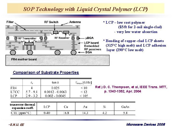
SOP Technology with Liquid Crystal Polymer (LCP) * LCP – low cost polymer ($5/ft for 2 -mil single-clad) - very low water absortion * Bonding of copper-clad LCP sheets (315°C high melt) and LCP adhesion layer (290°C low melt) Comparison of Substrate Properties Ref. ) D. C. Thompson, et al, IEEE Trans. MTT, p. 1343 -1352, Apr. 2004 transverse thermal expansion coeff. • S. N. U. EE Microwave Devices 2008

What is LTCC ( I )? Why LTCC (Low Temperature Co-Fired Ceramic) in RF ? LTCC - glass/alumina mixture that sinters at low temperature (< 900°C) ← highly conductive materials required for reducing loss in RF - W in HTCC [High Temperature (~1600ºC) Co-Fired Ceramic, Alumina] - Low-temperature firing (at ~ 850°C) enables the use of Ag, Au, Cu electrode LTCC Materials - Borosilicate glass + Al 2 O 3 (or mullite, cordierite) + organic binder : Al 2 O 3 : 20 -80%, B 2 O 3, Si. O 2: 10 -70% : the borosilicate component was added to the basic HTCC(Al 2 O 3) composition in order to decrease the sintering temperature - The role of Al 2 O 3 (or mullite, cordierite) - increase dielectric constant & strength - The decrease in dielectric constant can be attained by increasing glass content → raw LTCC delivered as a flexible sheet called “green tape” Electrode - Chemical compatibility (Typical material : Ag or Cu) - No interdiffusion between the electrode and LTCC substrate - No delamination due to the shrinkage mismatch and dewetting • S. N. U. EE Microwave Devices 2008

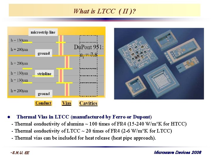
What is LTCC ( II )? Thermal Vias in LTCC (manufactured by Ferro or Dupont) - Thermal conductivity of alumina ~ 100 times of FR 4 (15 -240 W/m°K for HTCC) - Thermal conductivity of LTCC ~ 20 times of FR 4 (2 -6 W/m°K for LTCC) - Thermal vias can be included for heat release (heat pipe approach). • S. N. U. EE Microwave Devices 2008

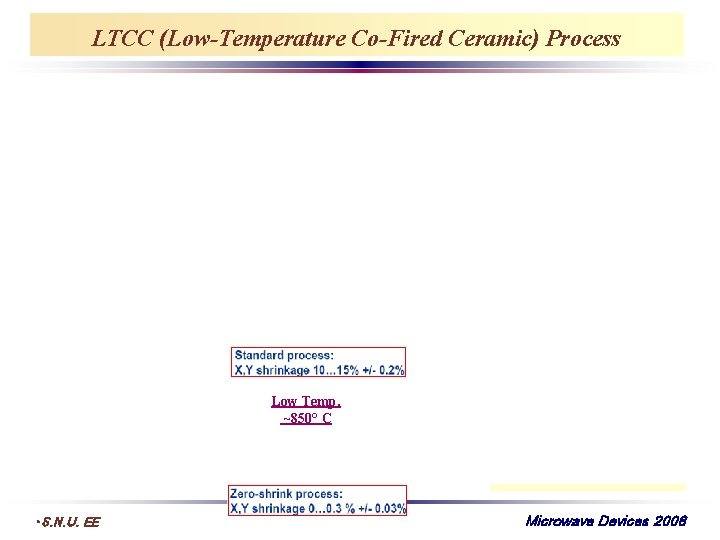
LTCC (Low-Temperature Co-Fired Ceramic) Process Low Temp. ~850° C • S. N. U. EE Microwave Devices 2008

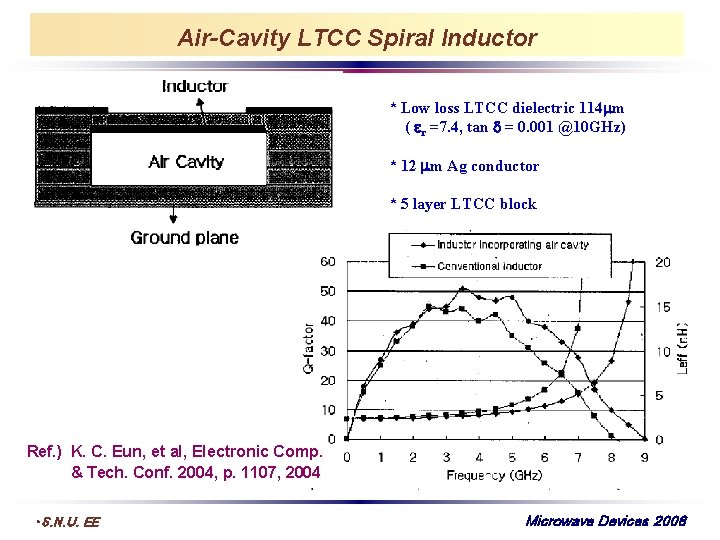
Air-Cavity LTCC Spiral Inductor * Low loss LTCC dielectric 114 m ( r =7. 4, tan = 0. 001 @10 GHz) * 12 m Ag conductor * 5 layer LTCC block Ref. ) K. C. Eun, et al, Electronic Comp. & Tech. Conf. 2004, p. 1107, 2004 • S. N. U. EE Microwave Devices 2008

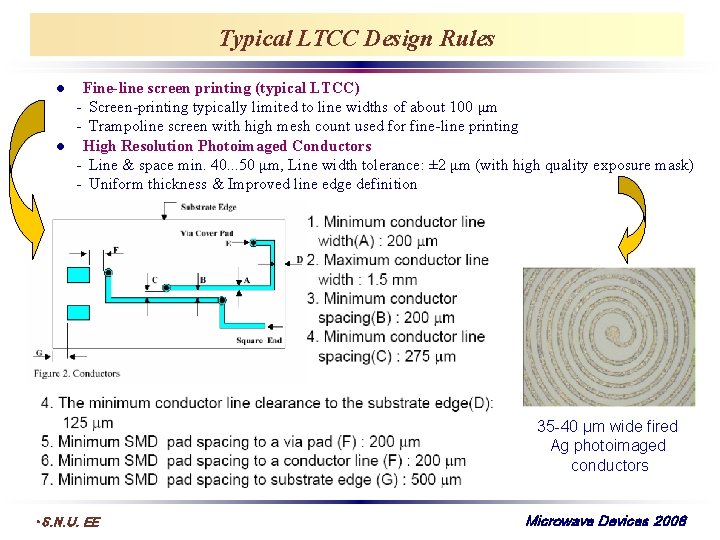
Typical LTCC Design Rules Fine-line screen printing (typical LTCC) - Screen-printing typically limited to line widths of about 100 μm - Trampoline screen with high mesh count used for fine-line printing High Resolution Photoimaged Conductors - Line & space min. 40. . . 50 μm, Line width tolerance: ± 2 μm (with high quality exposure mask) - Uniform thickness & Improved line edge definition 35 -40 μm wide fired Ag photoimaged conductors • S. N. U. EE Microwave Devices 2008

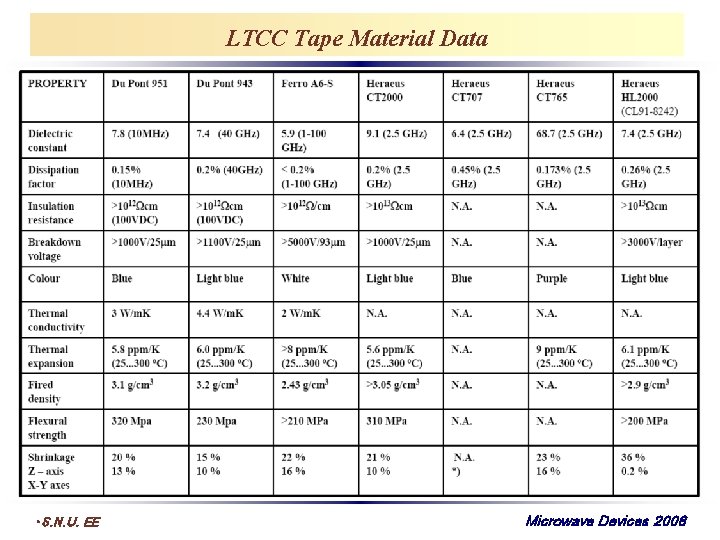
LTCC Tape Material Data • S. N. U. EE Microwave Devices 2008

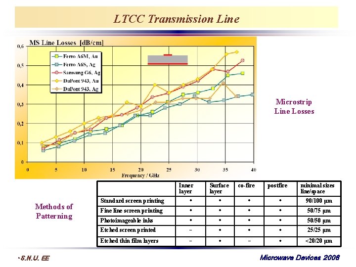
LTCC Transmission Line Microstrip Line Losses Inner layer Methods of Patterning • S. N. U. EE Surface layer co-fire postfire minimal sizes line/space Standard screen printing ● ● 90/100 μm Fine line screen printing ● ● 50/75 μm Photoimageable inks ● ● 50/50 μm Etched screen printed – ● ● ● 25/25 μm Etched thin film layers – ● <20/20 μm Microwave Devices 2008
![Future Directions of LTCC Technology Parameter 1998 2003 2009 Min via size μm 250 Future Directions of LTCC Technology Parameter 1998 2003 2009 Min. via size [μm] 250](https://slidetodoc.com/presentation_image_h2/0b4b280e62409c0847299affccbf09f1/image-26.jpg)
Future Directions of LTCC Technology Parameter 1998 2003 2009 Min. via size [μm] 250 40 - 25 Min. via pitch [μm] 500 125 75 Min. line width [μm] 125 20 15 Min. line pitch [μm] 250 40 30 Line density [cm/cm 2] 40 200 267 Max. module size [cm 2] 130 360 645 Max. working freq. [GHz] 10 38 80 Max. working temp. [°C] 125 160 200 Future Technologies on LTCC • New screens, inks and printing methods for fine line screen printing • Photoimageable LTCC-systems (conductor-, dielectric and resistor- inks and tapes) • Zero-shrinking including cavities and windows • Pressureless lamination • One process step for via forming and filling • Inks/tapes to integrate optical components • S. N. U. EE Microwave Devices 2008

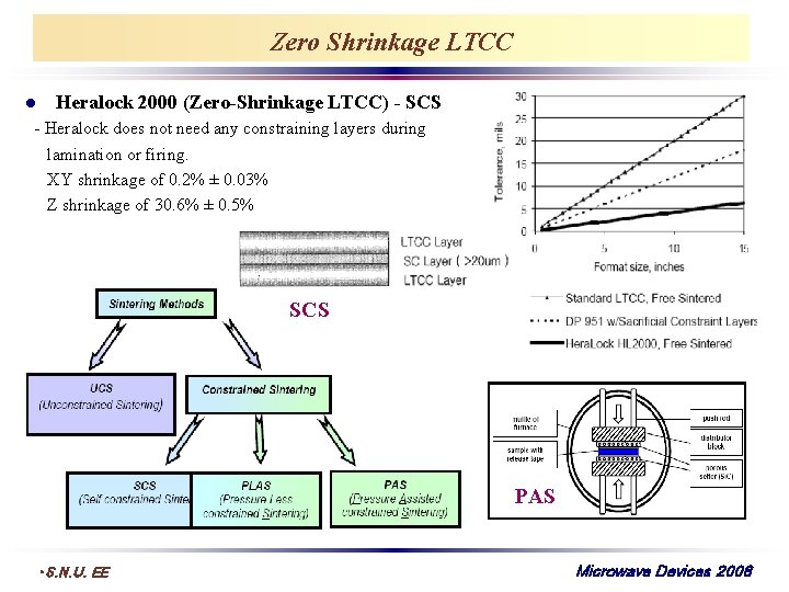
Zero Shrinkage LTCC Heralock 2000 (Zero-Shrinkage LTCC) - SCS - Heralock does not need any constraining layers during lamination or firing. XY shrinkage of 0. 2% ± 0. 03% Z shrinkage of 30. 6% ± 0. 5% SCS PAS • S. N. U. EE Microwave Devices 2008

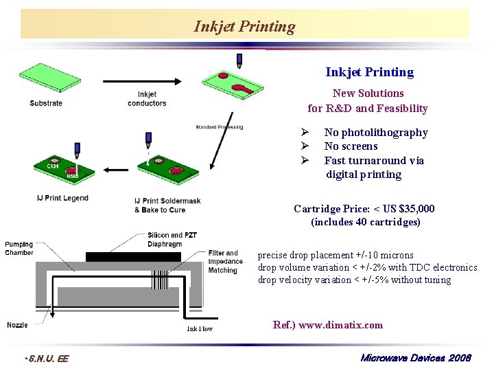
Inkjet Printing New Solutions for R&D and Feasibility Ø Ø Ø No photolithography No screens Fast turnaround via digital printing Cartridge Price: < US $35, 000 (includes 40 cartridges) precise drop placement +/-10 microns drop volume variation < +/-2% with TDC electronics drop velocity variation < +/-5% without tuning Ref. ) www. dimatix. com • S. N. U. EE Microwave Devices 2008

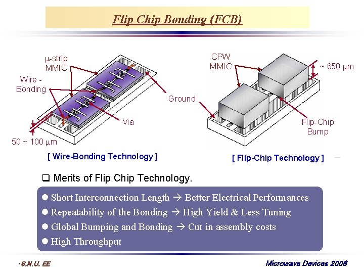
Flip Chip Bonding (FCB) CPW MMIC m-strip MMIC ~ 650 mm Wire Bonding Ground Via 50 ~ 100 mm [ Wire-Bonding Technology ] Flip-Chip Bump [ Flip-Chip Technology ] Merits of Flip Chip Technology. Short Interconnection Length Better Electrical Performances Repeatability of the Bonding High Yield & Less Tuning Global Bumping and Bonding Cut in assembly costs High Throughput • S. N. U. EE Microwave Devices 2008

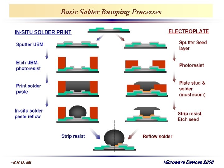
Basic Solder Bumping Processes • S. N. U. EE Microwave Devices 2008

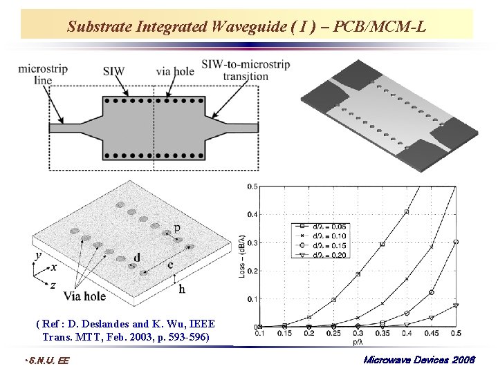
Substrate Integrated Waveguide ( I ) – PCB/MCM-L ( Ref : D. Deslandes and K. Wu, IEEE Trans. MTT, Feb. 2003, p. 593 -596) • S. N. U. EE Microwave Devices 2008

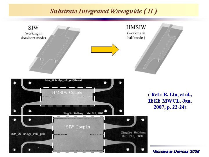
Substrate Integrated Waveguide ( II ) ( Ref : B. Liu, et al. , IEEE MWCL, Jan. 2007, p. 22 -24) • S. N. U. EE Microwave Devices 2008