Microwave Devices Microwave Semiconductor Devices 3 2008 1


 n Ga. As n+ Ga. As (Ref. ) 1.")

 E JS")


 for frequency tripler & Quintupler •")
 No compact sources exist")


- Slides: 28
Microwave Devices - Microwave Semiconductor Devices - 3 2008 / 1 학기 서광석 • S. N. U. EE Microwave Devices 2008
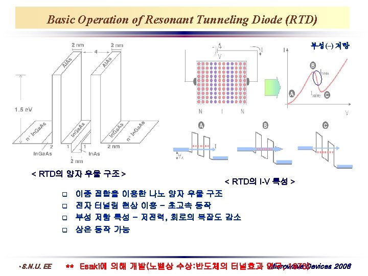
Microwave Diodes l Diodes for Signal Processing - Predistorter for linear amp. - Mixer/Frequency Multiplier - Switch n Schottky Diode n PIN Diode n Heterostructure Barrier Diode n Planar-Doped Barrier Diode l Diodes for Signal Sources (Oscillators) Gunn Diode n IMPATT Diode n Resonant Tunneling Diode n Varactor Diode n • S. N. U. EE Microwave Devices 2008
Diode Nonlinear Microwave Circuits diode frequency multiplier single-ended diode mixer • S. N. U. EE Microwave Devices 2008
Schottky Diode Metal (Schottky Contact) n Ga. As n+ Ga. As (Ref. ) 1. Sze, “Physics of Semiconductor Devices, ” Chap. 5 2. Rhoderick, “Metal-Semiconductor Metal (Ohmic Contact) Contacts” Vacuum level metal • S. N. U. EE n Ga. As Microwave Devices 2008
Schottky Diode의 Band Diagram <Zero bias> <Forward bias> X eee <Reverse bias> Small Leakage (~n. A) • S. N. U. EE Microwave Devices 2008
Schottky diode의 I-V 특성 * thermionic emission theory : 일반적(Ga. As, Si) E JS M N(E) WD <Forward bias> = effective Richardson constant (A* : include quantum mechanical correction) thermionic theory holds when • S. N. U. EE Microwave Devices 2008
Schottky Effect ~ 수십 m. V 측정 방법 • S. N. U. EE 1. I-V 특성 2. C-V 특성 3. (Photo-electron을 이용한 측정) Microwave Devices 2008
Schottky Diode의 구조 Ga. As의 Bn : 0. 7~0. 8 e. V Alx. Ga 1 -x. As 의 Bn : 0. 8~0. 9 e. V In 0. 53 Ga 0. 47 As 의 Bn : 0. 2 e. V (better for ohmic) In 0. 52 Al 0. 48 As 의 Bn : ~0. 5 e. V (증가 시킬 필요가 있음. ) * damage free process에 의한 q Bn= q( m- ) 를 구현하기 위한 연구가 진행. electrochemical plating에 의한 In. Al. As (/In. Ga. As)구조의 Pt Schottky diode (vertical) n (horizontal) n+ n+ n Rch S. I. Substrate • S. N. U. EE Rch에 의한 series 저항 문제 Microwave Devices 2008
Model of Schottky Diode Rch에 의한 series 저항 문제 RON/ROFF Rseries CJ Tera-Hertz Schottky diode – diode의 width를 0. 25 m 정도로 감소하여 Ron + Rseries ↓, cut-off frequency ↑ (contact pad는 air-bridge로 연결) • S. N. U. EE Microwave Devices 2008
Microwave Schottky Diode • S. N. U. EE Microwave Devices 2008
Membrane-Type Schottky Diode for 1. 5 THz Frequency Source Ref. : IEEE Trans. MTT, pp. 1538, 2004 • S. N. U. EE Microwave Devices 2008
PIN Diode Switch • S. N. U. EE Microwave Devices 2008
Principles of Transit Time Devices IMPATT ; INJ ~ 180º (IMPact ionization Avanche Transit Time) TUNNETT ; INJ ~ 90º (TUNNEel Transit Time) Ref. : IEEE Trans. MTT, pp. 760, 2002 • S. N. U. EE Microwave Devices 2008
Transit-Time Millimeter-wave Sources • S. N. U. EE Microwave Devices 2008
Gunn Millimeter-wave Sources • S. N. U. EE Microwave Devices 2008
RTD Millimeter-wave Sources • S. N. U. EE Microwave Devices 2008
Frequency Multiplier Millimeter-wave Sources Heterostructure Barrier Varactor (HBV) for frequency tripler & Quintupler • S. N. U. EE 3 W at 1. 7 THz with Schottky diode (2004) Microwave Devices 2008
Terahertz and Infrared Solid State Sources Quantum Cascade Laser (QCL) No compact sources exist for the generation of the LO power at 1 -10 THz. Ref. : M. Tonouchi, p. 97, Nature Photonics, 2007 • S. N. U. EE Microwave Devices 2008
Power Levels for Sub-Millimeterwave Oscillators 254 GHz/158μW, 346 GHz/25μW Oscillator MMICs with 35 nm In. P HEMT (In 0. 75 Ga 0. 25 As channel) - NGST, 2007 p. 223, IEEE MWCL • S. N. U. EE Microwave Devices 2008
Sub-Millimeterwave Receiver Performance FP : Fabry-Perot SHP : Sub-Harmonically Pumped 340 GHz/16 d. B gain LNA MMICs with 35 nm In. P HEMT (In 0. 75 Ga 0. 25 As channel) - NGST, 2007 • S. N. U. EE Microwave Devices 2008
Basic Principles of SIS Mixers • SIS: superconducting tunnel junction • SIS is a “submillimeter photodiode” – One electron per photon absorbed – “photon-assisted tunneling” • S. N. U. EE Microwave Devices 2008
Superconducting Bolometer for Terahertz Detection Cu/Nb metal stack Bolometer Array • S. N. U. EE Microwave Devices 2008
Fermi Level Pinning q Bn constant regardless of metal Various Models – Fermi-level pinning (Bardeen limit) Process의 영향 • Metal deposition process • Surface Preparation Method • Thermal annealing Ref. : H. Hasegawa, IPRM 1998, p. 451 • S. N. U. EE Microwave Devices 2008
Unified Defect Model for Schottky Barrier & Surface - X-ray photoelectron spectroscopy - MBE에서의 금속막 증착 에 의해 q B 측정 Ec n-type Ga. As EC ~ 0. 75 e. V q Bn ~ 0. 5 e. V p-type Ga. As EFm Ev 1. 42 e. V ~ 0. 75 e. V ~ 0. 5 e. V EFN ESA ESD EFP EN < Unified Defect Model for Ga. As > EF EV 5 10 15 20 deposited metal(Å) EC ( n-type Ga. As) OOOO ---Wsn n-Ga. As Surface of n-Ga. As ++++ OOOO Wsp p-Ga. As Surface of p-Ga. As * Model의 2개(+, -) level 존재는 이견이 없으나 level의 크기, 값에 대해서는 아직 논의/연구 • S. N. U. EE Microwave Devices 2008
Semi-Insulating Ga. As or In. P Substrate • S. N. U. EE Microwave Devices 2008
Undoped Ga. As Semi-Insulating Substrate • S. N. U. EE Microwave Devices 2008