MICROPROCESSORS ORGANIZATION OF 8085 Microprocessor 1 It is


- Slides: 41

MICROPROCESSORS & ORGANIZATION OF 8085

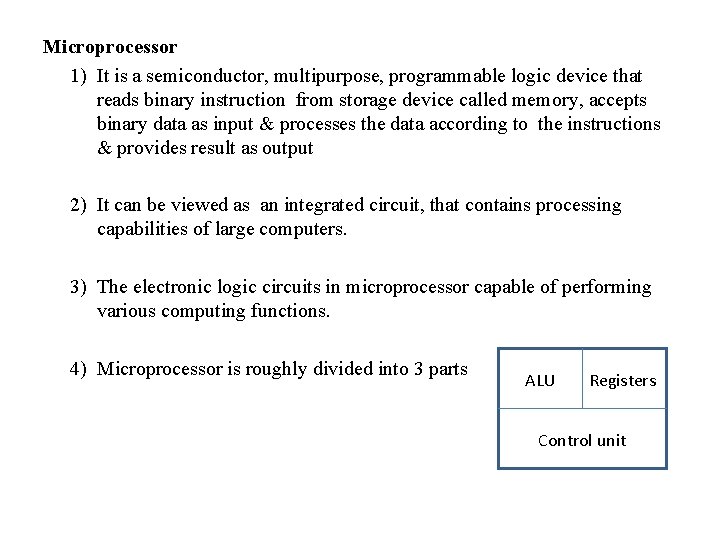
Microprocessor 1) It is a semiconductor, multipurpose, programmable logic device that reads binary instruction from storage device called memory, accepts binary data as input & processes the data according to the instructions & provides result as output 2) It can be viewed as an integrated circuit, that contains processing capabilities of large computers. 3) The electronic logic circuits in microprocessor capable of performing various computing functions. 4) Microprocessor is roughly divided into 3 parts ALU Registers Control unit

Functions 1) To fetch, decode & execute the instructions in proper order. 2) To transfer data from one block to another block or from one block to I/O lines 3) To give proper response to different external interrupts according to their priority. 4) To provide control & timing signals to the overall system according to the instructions

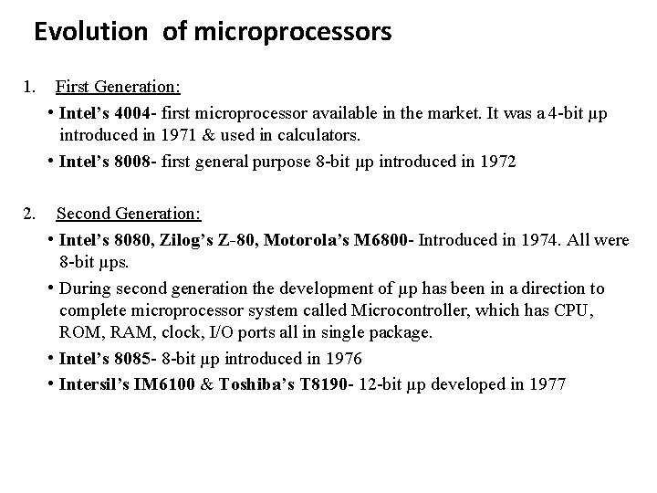
Evolution of microprocessors 1. First Generation: • Intel’s 4004 - first microprocessor available in the market. It was a 4 -bit µp introduced in 1971 & used in calculators. • Intel’s 8008 - first general purpose 8 -bit µp introduced in 1972 2. Second Generation: • Intel’s 8080, Zilog’s Z-80, Motorola’s M 6800 - Introduced in 1974. All were 8 -bit µps. • During second generation the development of µp has been in a direction to complete microprocessor system called Microcontroller, which has CPU, ROM, RAM, clock, I/O ports all in single package. • Intel’s 8085 - 8 -bit µp introduced in 1976 • Intersil’s IM 6100 & Toshiba’s T 8190 - 12 -bit µp developed in 1977

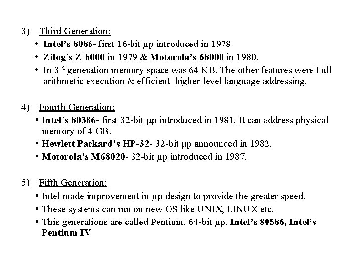
3) Third Generation: • Intel’s 8086 - first 16 -bit µp introduced in 1978 • Zilog’s Z-8000 in 1979 & Motorola’s 68000 in 1980. • In 3 rd generation memory space was 64 KB. The other features were Full arithmetic execution & efficient higher level language addressing. 4) Fourth Generation: • Intel’s 80386 - first 32 -bit µp introduced in 1981. It can address physical memory of 4 GB. • Hewlett Packard’s HP-32 - 32 -bit µp announced in 1982. • Motorola’s M 68020 - 32 -bit µp introduced in 1987. 5) Fifth Generation: • Intel made improvement in µp design to provide the greater speed. • These systems can run on new OS like UNIX, LINUX etc. • This generations are called Pentium. 64 -bit µp. Intel’s 80586, Intel’s Pentium IV


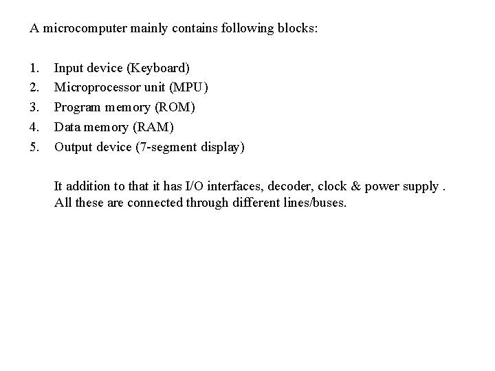
A microcomputer mainly contains following blocks: 1. 2. 3. 4. 5. Input device (Keyboard) Microprocessor unit (MPU) Program memory (ROM) Data memory (RAM) Output device (7 -segment display) It addition to that it has I/O interfaces, decoder, clock & power supply. All these are connected through different lines/buses.

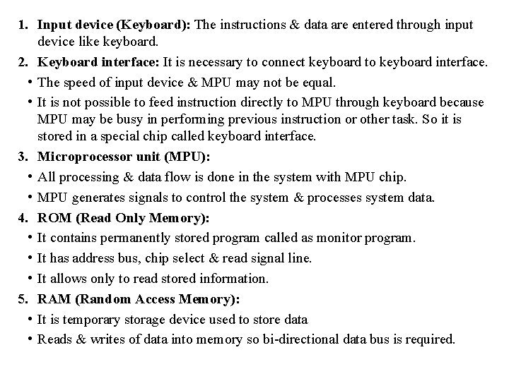
1. Input device (Keyboard): The instructions & data are entered through input device like keyboard. 2. Keyboard interface: It is necessary to connect keyboard to keyboard interface. • The speed of input device & MPU may not be equal. • It is not possible to feed instruction directly to MPU through keyboard because MPU may be busy in performing previous instruction or other task. So it is stored in a special chip called keyboard interface. 3. Microprocessor unit (MPU): • All processing & data flow is done in the system with MPU chip. • MPU generates signals to control the system & processes system data. 4. ROM (Read Only Memory): • It contains permanently stored program called as monitor program. • It has address bus, chip select & read signal line. • It allows only to read stored information. 5. RAM (Random Access Memory): • It is temporary storage device used to store data • Reads & writes of data into memory so bi-directional data bus is required.

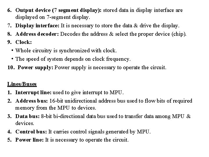
6. Output device (7 segment display): stored data in display interface are displayed on 7 -segment display. 7. Display interface: It is necessary to store the data & drive the display. 8. Address decoder: Decodes the address & select the proper device (chip). 9. Clock: • Whole circuitry is synchronized with clock. • The speed of system depends on clock frequency. 10. Power supply: Power supply is necessary to operate the circuit. Lines/Buses 1. Interrupt line: used to give interrupt to MPU. 2. Address bus: 16 -bit unidirectional address bus used to flow bits of required memory from the MPU to devices. 3. Data bus: 8 -bit bi-directional data bus used to transfer data among MPU & devices. 4. Control bus: It carries control signals generated by MPU. 5. Power line: It is necessary to operate the circuit.


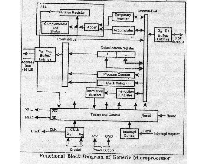
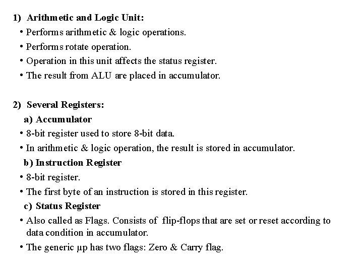
1) Arithmetic and Logic Unit: • Performs arithmetic & logic operations. • Performs rotate operation. • Operation in this unit affects the status register. • The result from ALU are placed in accumulator. 2) Several Registers: a) Accumulator • 8 -bit register used to store 8 -bit data. • In arithmetic & logic operation, the result is stored in accumulator. b) Instruction Register • 8 -bit register. • The first byte of an instruction is stored in this register. c) Status Register • Also called as Flags. Consists of flip-flops that are set or reset according to data condition in accumulator. • The generic µp has two flags: Zero & Carry flag.

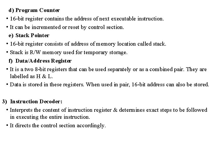
d) Program Counter • 16 -bit register contains the address of next executable instruction. • It can be incremented or reset by control section. e) Stack Pointer • 16 -bit register consists of address of memory location called stack. • Stack is R/W memory used for temporary storage. f) Data/Address Register • It is a two 8 -bit registers that can be used separately or as a combined pair. They are labelled as H & L. • Data is stored in these registers. When used in pair, 16 -bit address can also be stored. 3) Instruction Decoder: • Interprets the content of instruction register & determines exact steps to be followed in executing the entire instruction. • It directs the control section accordingly.

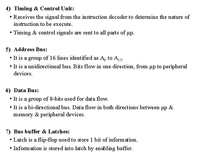
4) Timing & Control Unit: • Receives the signal from the instruction decoder to determine the nature of instruction to be execute. • Timing & control signals are sent to all parts of µp. 5) Address Bus: • It is a group of 16 lines identified as A 0 to A 15. • It is a unidirectional bus. Bits flow in one direction, from µp to peripheral devices. 6) Data Bus: • It is a group of 8 -bits used for data flow. • It is a bi-directional bus. Data flow in both directions between µp & memory & peripheral devices. 7) Bus buffer & Latches: • Latch is a flip-flop used to store 1 bit of information. • Information is stored into latch by enabling buffer.

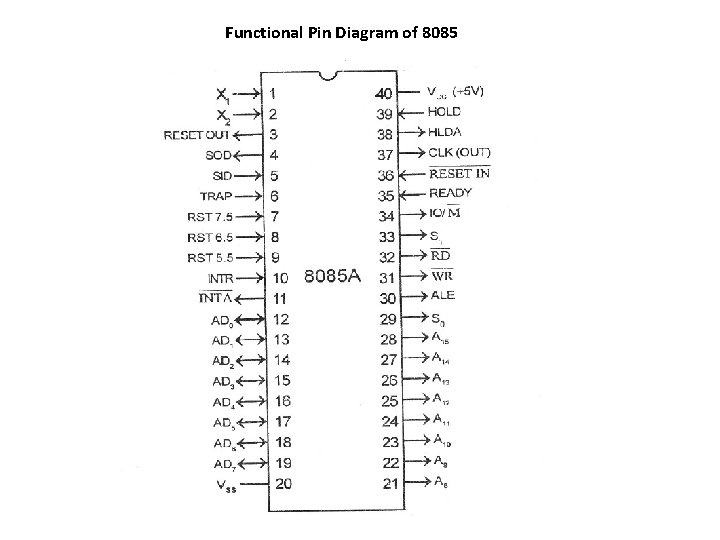
Functional Pin Diagram of 8085

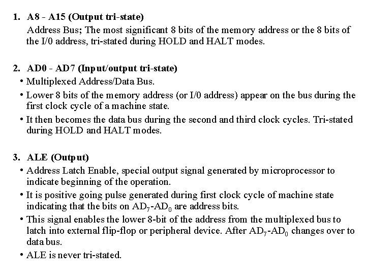
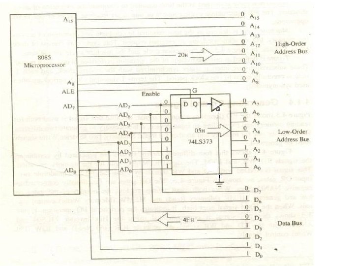
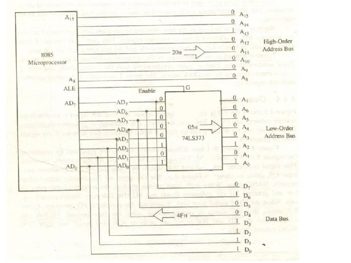
1. A 8 - A 15 (Output tri-state) Address Bus; The most significant 8 bits of the memory address or the 8 bits of the I/0 address, tri-stated during HOLD and HALT modes. 2. AD 0 - AD 7 (Input/output tri-state) • Multiplexed Address/Data Bus. • Lower 8 bits of the memory address (or I/0 address) appear on the bus during the first clock cycle of a machine state. • It then becomes the data bus during the second and third clock cycles. Tri-stated during HOLD and HALT modes. 3. ALE (Output) • Address Latch Enable, special output signal generated by microprocessor to indicate beginning of the operation. • It is positive going pulse generated during first clock cycle of machine state indicating that the bits on AD 7 -AD 0 are address bits. • This signal enables the lower 8 -bit of the address from the multiplexed bus to latch into external flip-flop or peripheral device. After AD 7 -AD 0 changes over to data bus. • ALE is never tri-stated.

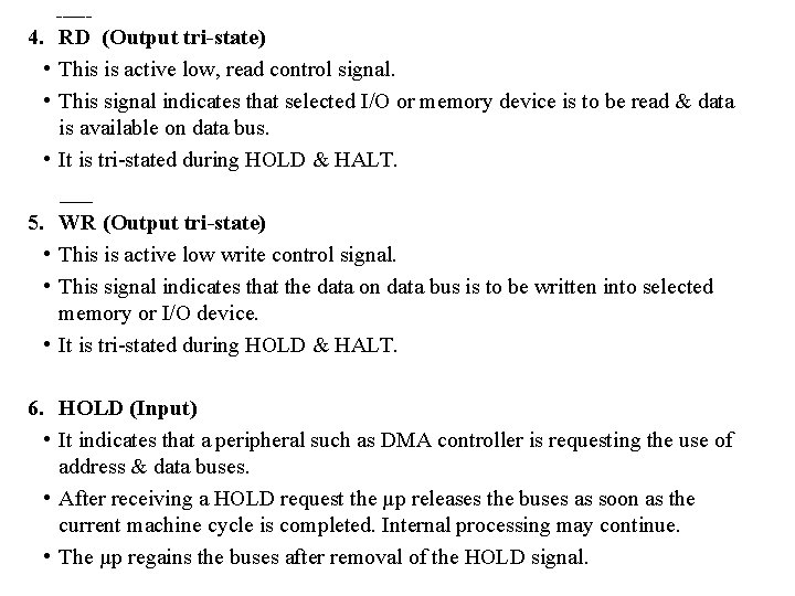
______ 4. RD (Output tri-state) • This is active low, read control signal. • This signal indicates that selected I/O or memory device is to be read & data is available on data bus. • It is tri-stated during HOLD & HALT. ___ 5. WR (Output tri-state) • This is active low write control signal. • This signal indicates that the data on data bus is to be written into selected memory or I/O device. • It is tri-stated during HOLD & HALT. 6. HOLD (Input) • It indicates that a peripheral such as DMA controller is requesting the use of address & data buses. • After receiving a HOLD request the µp releases the buses as soon as the current machine cycle is completed. Internal processing may continue. • The µp regains the buses after removal of the HOLD signal.

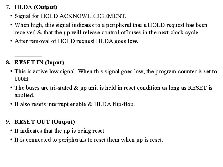
7. HLDA (Output) • Signal for HOLD ACKNOWLEDGEMENT. • When high, this signal indicates to a peripheral that a HOLD request has been received & that the µp will release control of buses in the next clock cycle. • After removal of HOLD request HLDA goes low. ___________ 8. RESET IN (Input) • This is active low signal. When this signal goes low, the program counter is set to 000 H • The buses are tri-stated & µp unit is held in reset condition as long as RESET is applied. • It also resets interrupt enable & HLDA flip-flop. 9. RESET OUT (Output) • It indicates that the µp is being reset. • It is connected to peripherals to reset them when µp is reset.

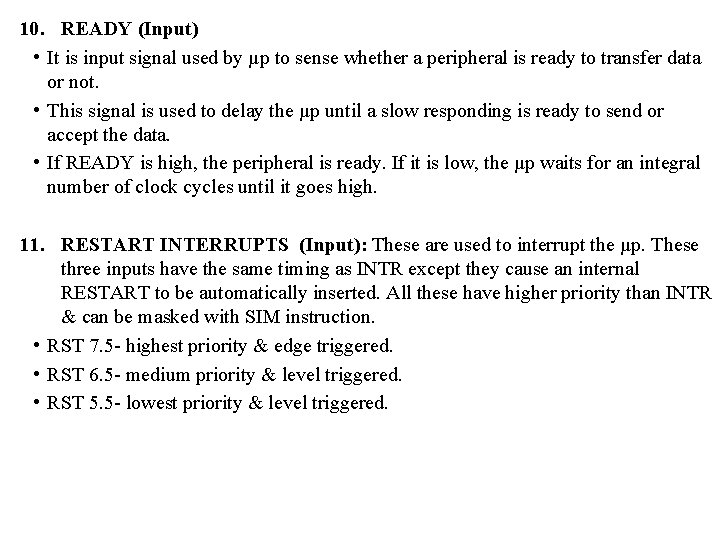
10. READY (Input) • It is input signal used by µp to sense whether a peripheral is ready to transfer data or not. • This signal is used to delay the µp until a slow responding is ready to send or accept the data. • If READY is high, the peripheral is ready. If it is low, the µp waits for an integral number of clock cycles until it goes high. 11. RESTART INTERRUPTS (Input): These are used to interrupt the µp. These three inputs have the same timing as INTR except they cause an internal RESTART to be automatically inserted. All these have higher priority than INTR & can be masked with SIM instruction. • RST 7. 5 - highest priority & edge triggered. • RST 6. 5 - medium priority & level triggered. • RST 5. 5 - lowest priority & level triggered.

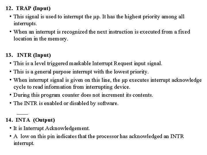
12. TRAP (Input) • This signal is used to interrupt the µp. It has the highest priority among all interrupts. • When an interrupt is recognized the next instruction is executed from a fixed location in the memory. 13. INTR (Input) • This is a level triggered maskable Interrupt Request input signal. • This is a general purpose interrupt with the lowest priority. • When interrupt signal is given on this line, the µp executes interrupt acknowledge cycle to read information from interrupting device. • During this program counter does not increment its contents. • The INTR is enabled or disabled by software. ____ 14. INTA (Output) • It is Interrupt Acknowledgement. • A low on this pin indicates that the processor has acknowledged an INTR interrupt.

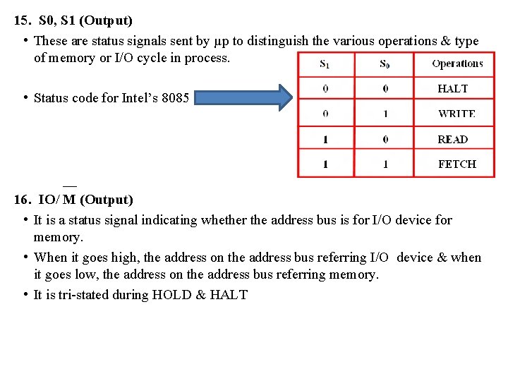
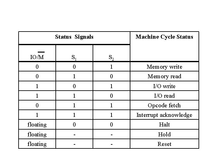
15. S 0, S 1 (Output) • These are status signals sent by µp to distinguish the various operations & type of memory or I/O cycle in process. • Status code for Intel’s 8085 __ 16. IO/ M (Output) • It is a status signal indicating whether the address bus is for I/O device for memory. • When it goes high, the address on the address bus referring I/O device & when it goes low, the address on the address bus referring memory. • It is tri-stated during HOLD & HALT

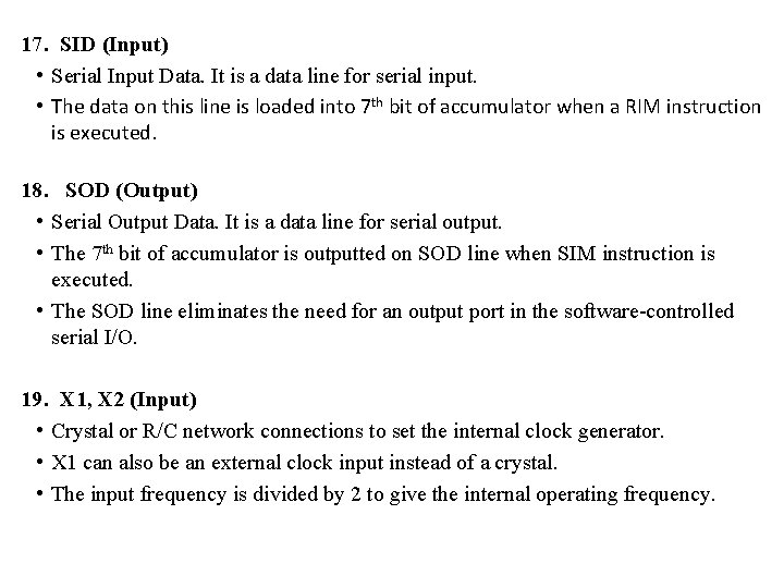
17. SID (Input) • Serial Input Data. It is a data line for serial input. • The data on this line is loaded into 7 th bit of accumulator when a RIM instruction is executed. 18. SOD (Output) • Serial Output Data. It is a data line for serial output. • The 7 th bit of accumulator is outputted on SOD line when SIM instruction is executed. • The SOD line eliminates the need for an output port in the software-controlled serial I/O. 19. X 1, X 2 (Input) • Crystal or R/C network connections to set the internal clock generator. • X 1 can also be an external clock input instead of a crystal. • The input frequency is divided by 2 to give the internal operating frequency.

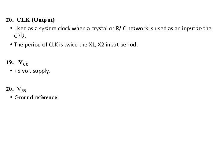
20. CLK (Output) • Used as a system clock when a crystal or R/ C network is used as an input to the CPU. • The period of CLK is twice the X 1, X 2 input period. 19. VCC • +5 volt supply. 20. VSS • Ground reference.


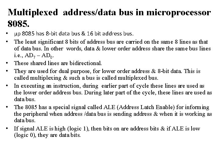
Multiplexed address/data bus in microprocessor 8085. • µp 8085 has 8 -bit data bus & 16 bit address bus. • The least significant 8 bits of address bus are carried on the same 8 lines as that of data bus. In other words, data & lower order address share the same bus lines i. e. , AD 7 – AD 0. • These shared lines are bidirectional. • They are used for dual purpose, for lower order address & 8 -bit data. This is called multiplexing & such a bus is called multiplexed bus. • In executing an instruction, during earlier part of cycle these lines are used as the lower order address bus. During later part of the cycle, these lines are used as data bus. • The 8085 has a special signal called ALE (Address Latch Enable) for informing the peripheral when address /data bus is sending address & when it is working as data bus. • If signal ALE is high (logic 1), then bits on are address bits & if ALE is low (logic 0), they are data bits.


MAIN PROGRAM Statement 1 Statement 2 Statement 3 Interrupt Statement 4 Statement 5 ISR

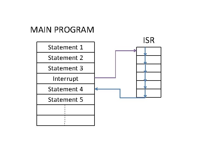
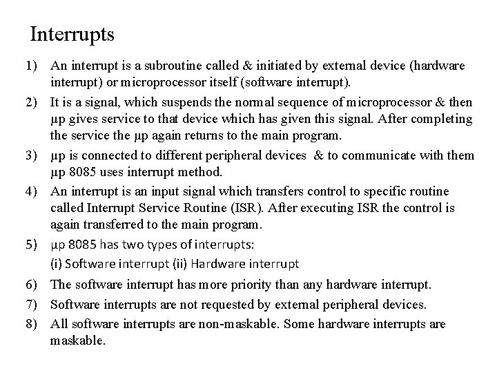
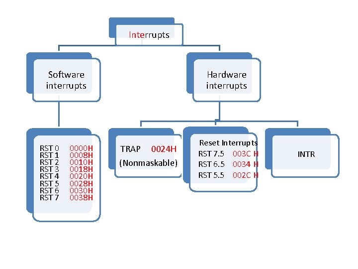
Interrupts 1) An interrupt is a subroutine called & initiated by external device (hardware interrupt) or microprocessor itself (software interrupt). 2) It is a signal, which suspends the normal sequence of microprocessor & then µp gives service to that device which has given this signal. After completing the service the µp again returns to the main program. 3) µp is connected to different peripheral devices & to communicate with them µp 8085 uses interrupt method. 4) An interrupt is an input signal which transfers control to specific routine called Interrupt Service Routine (ISR). After executing ISR the control is again transferred to the main program. 5) µp 8085 has two types of interrupts: (i) Software interrupt (ii) Hardware interrupt 6) The software interrupt has more priority than any hardware interrupt. 7) Software interrupts are not requested by external peripheral devices. 8) All software interrupts are non-maskable. Some hardware interrupts are maskable.

Interrupts Software interrupts RST 0 RST 1 RST 2 RST 3 RST 4 RST 5 RST 6 RST 7 0000 H 0008 H 0010 H 0018 H 0020 H 0028 H 0030 H 0038 H Hardware interrupts TRAP 0024 H (Nonmaskable) Reset Interrupts RST 7. 5 003 C H RST 6. 5 0034 H RST 5. 5 002 C H INTR

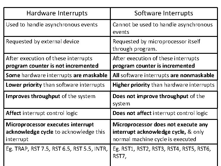
Hardware Interrupts Software Interrupts Used to handle asynchronous events Cannot be used to handle asynchronous events Requested by external device Requested by microprocessor itself through program. After execution of these interrupts program counter is not incremented After execution of these interrupts program counter is incremented Some hardware interrupts are maskable All software interrupts are nonmaskable Lower priority than software interrupts Higher priority than hardware interrupts Improves throughput of the system Does not improve throughput of the system Affect interrupt control logic Does not affect interrupt control logic Microprocessor executes interrupt acknowledge cycle to acknowledge this interrupt Microprocessor does not execute any interrupt acknowledge cycle, & only normal machine cycle is executed Eg. TRAP, RST 7. 5, RST 6. 5, RST 5. 5, INTR, Eg. RST 1, RST 2, RST 3, RST 4, RST 5, RST 6, RST 7,

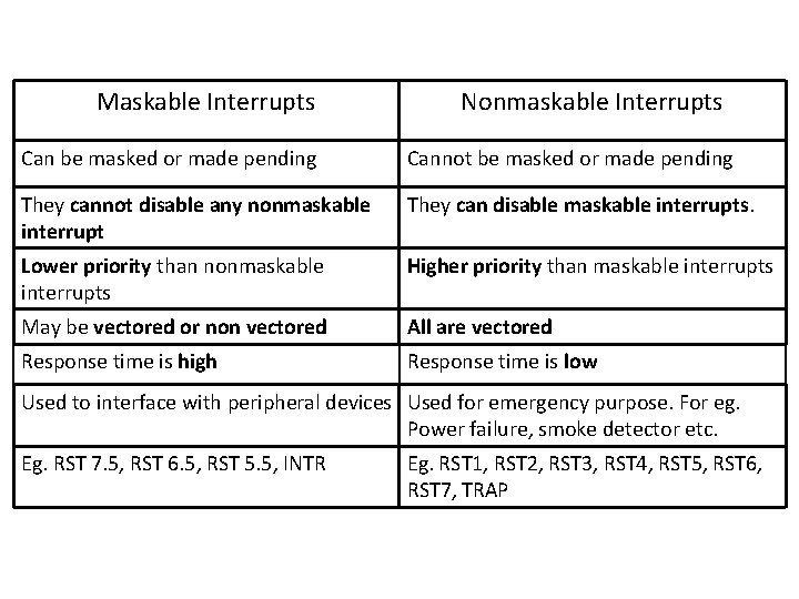
Maskable Interrupts Nonmaskable Interrupts Can be masked or made pending Cannot be masked or made pending They cannot disable any nonmaskable interrupt They can disable maskable interrupts. Lower priority than nonmaskable interrupts Higher priority than maskable interrupts May be vectored or non vectored All are vectored Response time is high Response time is low Used to interface with peripheral devices Used for emergency purpose. For eg. Power failure, smoke detector etc. Eg. RST 7. 5, RST 6. 5, RST 5. 5, INTR Eg. RST 1, RST 2, RST 3, RST 4, RST 5, RST 6, RST 7, TRAP

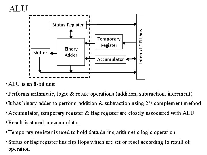
ALU Shifter Binary Adder Temporary Register Accumulator Internal CPU bus Status Register • ALU is an 8 -bit unit • Performs arithmetic, logic & rotate operations (addition, subtraction, increment) • It has binary adder to perform addition & subtraction using 2’s complement method • Accumulator, temporary register & flag register are closely associated with ALU • Result is stored in accumulator • Temporary register is used to hold data during arithmetic logic operation • Status or flag register has flip flops which are set or reset according to result of operation


• Shifter performs rotate left, rotate right operation. • Adder performs arithmetic operations like addition, subtraction, increment, decrement etc.

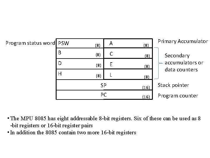
Program status word PSW (8) A (8) B (8) C (8) D (8) E (8) H (8) L (8) Primary Accumulator Secondary accumulators or data counters SP (16) Stack pointer PC (16) Program counter • The MPU 8085 has eight addressable 8 -bit registers. Six of these can be used as 8 -bit registers or 16 -bit register pairs • In addition the 8085 contain two more 16 -bit registers

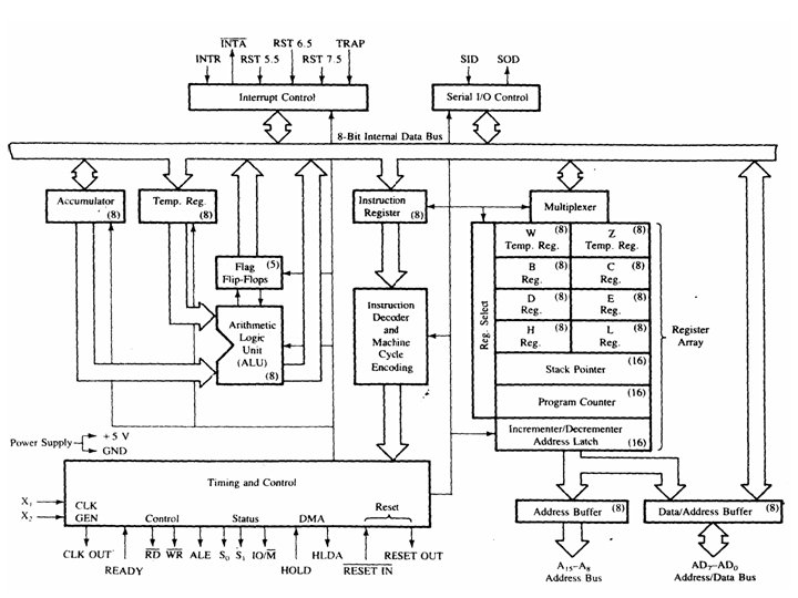
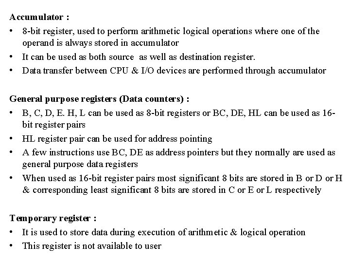
Accumulator : • 8 -bit register, used to perform arithmetic logical operations where one of the operand is always stored in accumulator • It can be used as both source as well as destination register. • Data transfer between CPU & I/O devices are performed through accumulator General purpose registers (Data counters) : • B, C, D, E. H, L can be used as 8 -bit registers or BC, DE, HL can be used as 16 bit register pairs • HL register pair can be used for address pointing • A few instructions use BC, DE as address pointers but they normally are used as general purpose data registers • When used as 16 -bit register pairs most significant 8 bits are stored in B or D or H & corresponding least significant 8 bits are stored in C or E or L respectively Temporary register : • It is used to store data during execution of arithmetic & logical operation • This register is not available to user

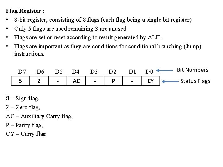
Flag Register : • 8 -bit register, consisting of 8 flags (each flag being a single bit register). • Only 5 flags are used remaining 3 are unused. • Flags are set or reset according to result generated by ALU. • Flags are important as they are conditions for conditional branching (Jump) instructions. D 7 D 6 D 5 D 4 D 3 D 2 D 1 D 0 S Z - AC - P - CY S – Sign flag, Z – Zero flag, AC – Auxiliary Carry flag, P – Parity flag, CY – Carry flag Bit Numbers Status Flags

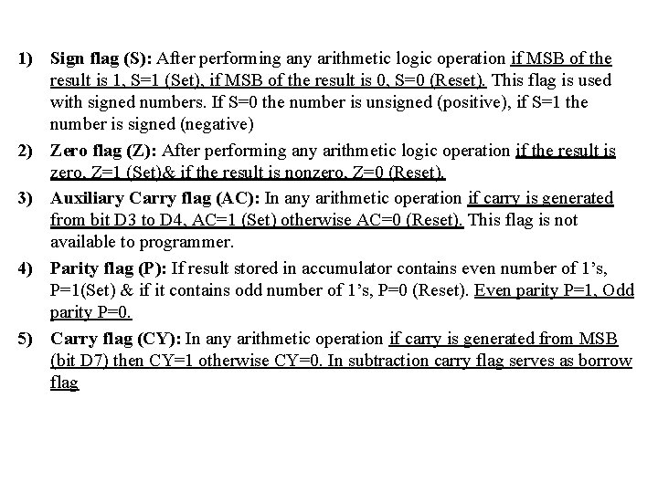
1) Sign flag (S): After performing any arithmetic logic operation if MSB of the result is 1, S=1 (Set), if MSB of the result is 0, S=0 (Reset). This flag is used with signed numbers. If S=0 the number is unsigned (positive), if S=1 the number is signed (negative) 2) Zero flag (Z): After performing any arithmetic logic operation if the result is zero, Z=1 (Set)& if the result is nonzero, Z=0 (Reset). 3) Auxiliary Carry flag (AC): In any arithmetic operation if carry is generated from bit D 3 to D 4, AC=1 (Set) otherwise AC=0 (Reset). This flag is not available to programmer. 4) Parity flag (P): If result stored in accumulator contains even number of 1’s, P=1(Set) & if it contains odd number of 1’s, P=0 (Reset). Even parity P=1, Odd parity P=0. 5) Carry flag (CY): In any arithmetic operation if carry is generated from MSB (bit D 7) then CY=1 otherwise CY=0. In subtraction carry flag serves as borrow flag

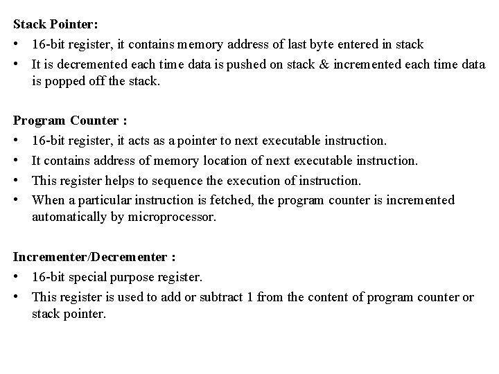
Stack Pointer: • 16 -bit register, it contains memory address of last byte entered in stack • It is decremented each time data is pushed on stack & incremented each time data is popped off the stack. Program Counter : • 16 -bit register, it acts as a pointer to next executable instruction. • It contains address of memory location of next executable instruction. • This register helps to sequence the execution of instruction. • When a particular instruction is fetched, the program counter is incremented automatically by microprocessor. Incrementer/Decrementer : • 16 -bit special purpose register. • This register is used to add or subtract 1 from the content of program counter or stack pointer.

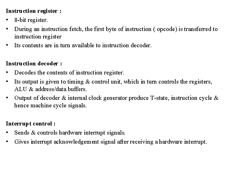
Instruction register : • 8 -bit register. • During an instruction fetch, the first byte of instruction ( opcode) is transferred to instruction register • Its contents are in turn available to instruction decoder. Instruction decoder : • Decodes the contents of instruction register. • Its output is given to timing & control unit, which in turn controls the registers, ALU & address/data buffers. • Output of decoder & internal clock generator produce T-state, instruction cycle & hence machine cycle signals. Interrupt control : • Sends & controls hardware interrupt signals. • Gives interrupt acknowledgement signal after receiving a hardware interrupt.

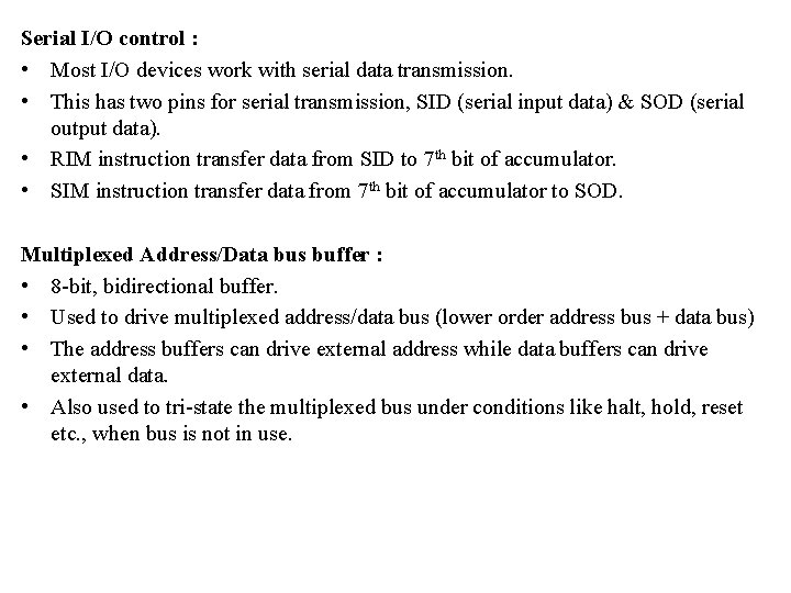
Serial I/O control : • Most I/O devices work with serial data transmission. • This has two pins for serial transmission, SID (serial input data) & SOD (serial output data). • RIM instruction transfer data from SID to 7 th bit of accumulator. • SIM instruction transfer data from 7 th bit of accumulator to SOD. Multiplexed Address/Data bus buffer : • 8 -bit, bidirectional buffer. • Used to drive multiplexed address/data bus (lower order address bus + data bus) • The address buffers can drive external address while data buffers can drive external data. • Also used to tri-state the multiplexed bus under conditions like halt, hold, reset etc. , when bus is not in use.

Status Signals Machine Cycle Status IO/M S 1 S 2 0 0 1 Memory write 0 1 0 Memory read 1 0 1 I/O write 1 1 0 I/O read 0 1 1 Opcode fetch 1 1 1 Interrupt acknowledge floating 0 0 Halt floating - - Hold floating - - Reset