ELEC 7770 Advanced VLSI Design Spring 2008 Verification
- Slides: 49

ELEC 7770 Advanced VLSI Design Spring 2008 Verification Vishwani D. Agrawal James J. Danaher Professor ECE Department, Auburn University Auburn, AL 36849 vagrawal@eng. auburn. edu http: //www. eng. auburn. edu/~vagrawal/COURSE/E 7770_Spr 10/course. html Spring 2010, Jan 15. . ELEC 7770: Advanced VLSI Design (Agrawal) 1

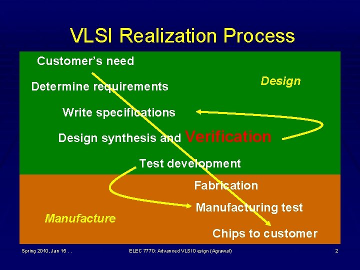
VLSI Realization Process Customer’s need Design Determine requirements Write specifications Design synthesis and Verification Test development Fabrication Manufacture Manufacturing test Chips to customer Spring 2010, Jan 15. . ELEC 7770: Advanced VLSI Design (Agrawal) 2

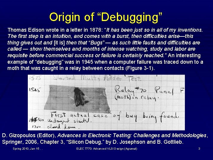
Origin of “Debugging” Thomas Edison wrote in a letter in 1878: “It has been just so in all of my inventions. The first step is an intuition, and comes with a burst, then difficulties arise—this thing gives out and [it is] then that “Bugs” — as such little faults and difficulties are called — show themselves and months of intense watching, study and labor are requisite before commercial success or failure is certainly reached. ” An interesting example of “debugging” was in 1945 when a computer failure was traced down to a moth that was caught in a relay between contacts (Figure 3 -1). D. Gizopoulos (Editor), Advances in Electronic Testing: Challenges and Methodologies, Springer, 2006, Chapter 3, “Silicon Debug, ” by D. Josephson and B. Gottlieb. Spring 2010, Jan 15. . ELEC 7770: Advanced VLSI Design (Agrawal) 3

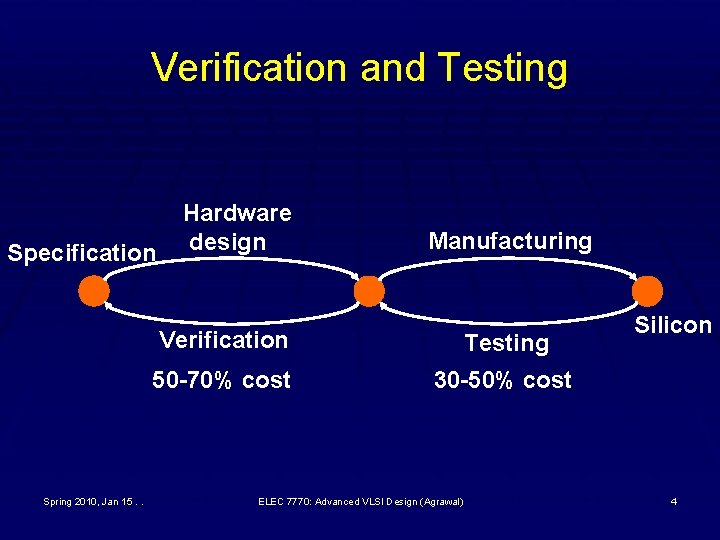
Verification and Testing Specification Spring 2010, Jan 15. . Hardware design Manufacturing Verification Testing 50 -70% cost 30 -50% cost ELEC 7770: Advanced VLSI Design (Agrawal) Silicon 4

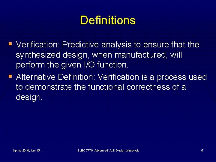
Definitions § Verification: Predictive analysis to ensure that the § synthesized design, when manufactured, will perform the given I/O function. Alternative Definition: Verification is a process used to demonstrate the functional correctness of a design. Spring 2010, Jan 15. . ELEC 7770: Advanced VLSI Design (Agrawal) 5

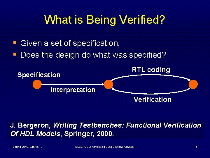
What is Being Verified? § Given a set of specification, § Does the design do what was specified? RTL coding Specification Interpretation Verification J. Bergeron, Writing Testbenches: Functional Verification Of HDL Models, Springer, 2000. Spring 2010, Jan 15. . ELEC 7770: Advanced VLSI Design (Agrawal) 6

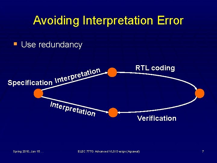
Avoiding Interpretation Error § Use redundancy r p r e t Specification In n o i t a t e Interp retati on Spring 2010, Jan 15. . RTL coding Verification ELEC 7770: Advanced VLSI Design (Agrawal) 7

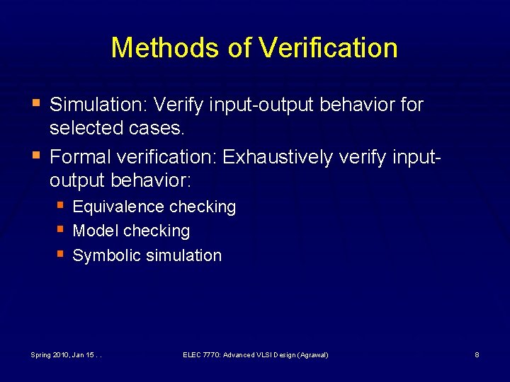
Methods of Verification § Simulation: Verify input-output behavior for § selected cases. Formal verification: Exhaustively verify inputoutput behavior: § Equivalence checking § Model checking § Symbolic simulation Spring 2010, Jan 15. . ELEC 7770: Advanced VLSI Design (Agrawal) 8

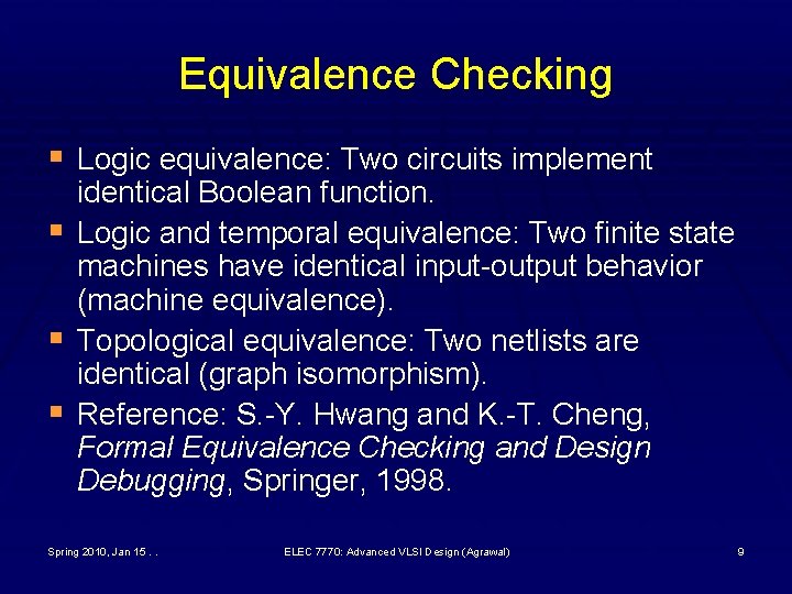
Equivalence Checking § Logic equivalence: Two circuits implement § § § identical Boolean function. Logic and temporal equivalence: Two finite state machines have identical input-output behavior (machine equivalence). Topological equivalence: Two netlists are identical (graph isomorphism). Reference: S. -Y. Hwang and K. -T. Cheng, Formal Equivalence Checking and Design Debugging, Springer, 1998. Spring 2010, Jan 15. . ELEC 7770: Advanced VLSI Design (Agrawal) 9

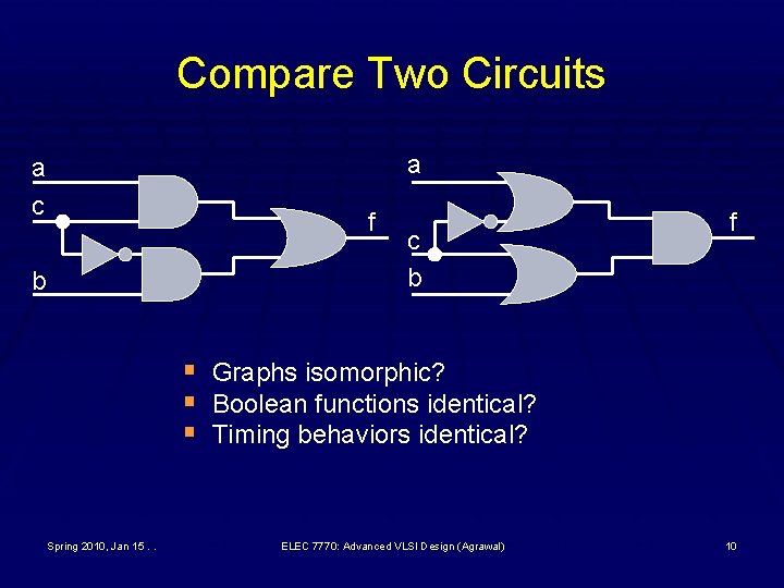
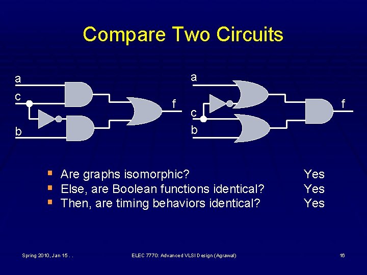
Compare Two Circuits a a c f b § § § Spring 2010, Jan 15. . c b f Graphs isomorphic? Boolean functions identical? Timing behaviors identical? ELEC 7770: Advanced VLSI Design (Agrawal) 10

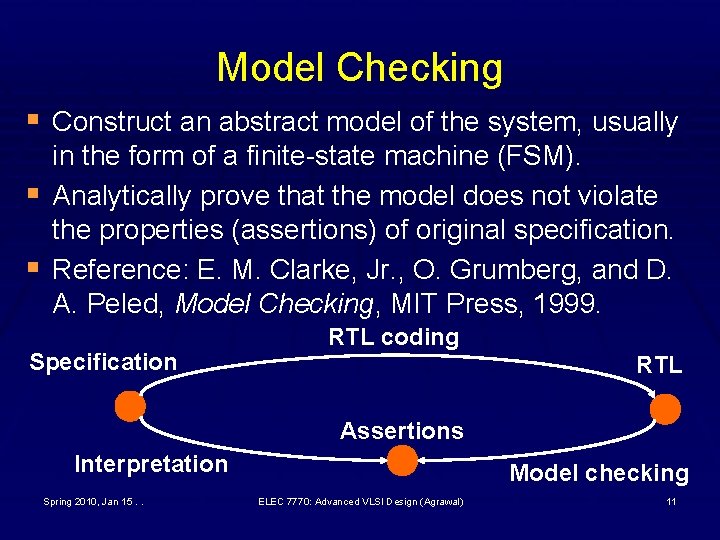
Model Checking § Construct an abstract model of the system, usually § § in the form of a finite-state machine (FSM). Analytically prove that the model does not violate the properties (assertions) of original specification. Reference: E. M. Clarke, Jr. , O. Grumberg, and D. A. Peled, Model Checking, MIT Press, 1999. Specification RTL coding RTL Assertions Interpretation Spring 2010, Jan 15. . Model checking ELEC 7770: Advanced VLSI Design (Agrawal) 11

Symbolic Simulation § Simulation with algebraic symbols rather than § § numerical values. Self-consistency: A complex (more advanced) design produces the same result as a much simpler (and previously verified) design. Reference: R. B. Jones, Symbolic Simulation Methods for Industrial Formal Verification, Springer, 2002. Spring 2010, Jan 15. . ELEC 7770: Advanced VLSI Design (Agrawal) 12

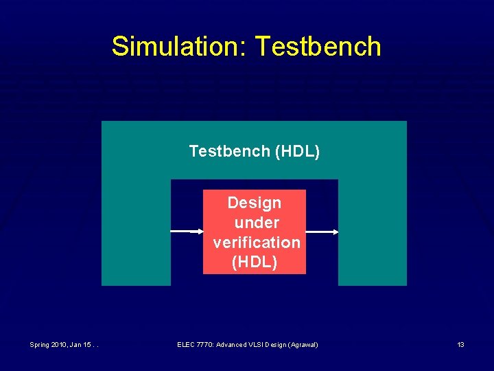
Simulation: Testbench (HDL) Design under verification (HDL) Spring 2010, Jan 15. . ELEC 7770: Advanced VLSI Design (Agrawal) 13

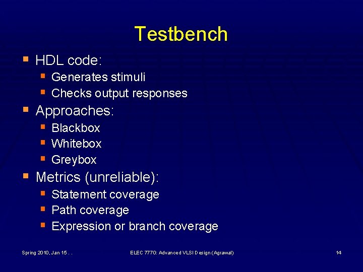
Testbench § HDL code: § Generates stimuli § Checks output responses § Approaches: § Blackbox § Whitebox § Greybox § Metrics (unreliable): § Statement coverage § Path coverage § Expression or branch coverage Spring 2010, Jan 15. . ELEC 7770: Advanced VLSI Design (Agrawal) 14

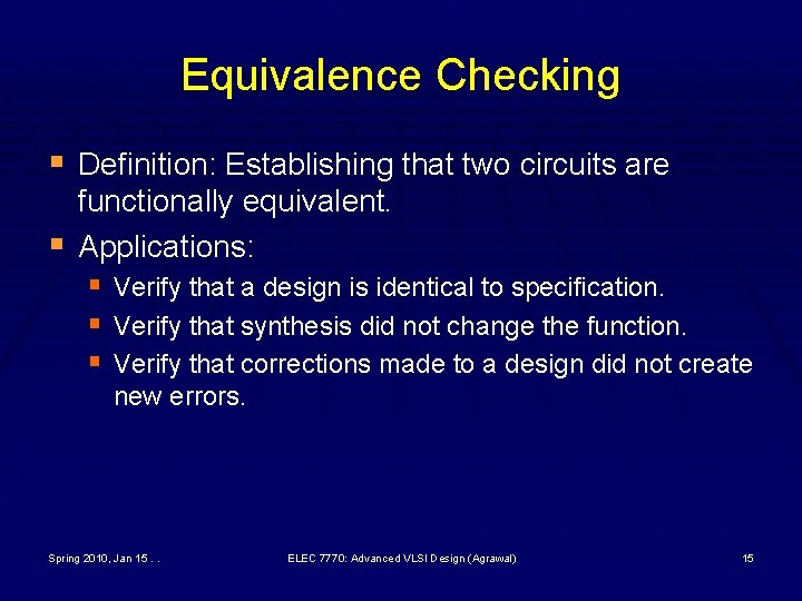
Equivalence Checking § Definition: Establishing that two circuits are § functionally equivalent. Applications: § Verify that a design is identical to specification. § Verify that synthesis did not change the function. § Verify that corrections made to a design did not create new errors. Spring 2010, Jan 15. . ELEC 7770: Advanced VLSI Design (Agrawal) 15

Compare Two Circuits a a c f b § § § c b Are graphs isomorphic? Else, are Boolean functions identical? Then, are timing behaviors identical? Spring 2010, Jan 15. . f ELEC 7770: Advanced VLSI Design (Agrawal) Yes Yes 16

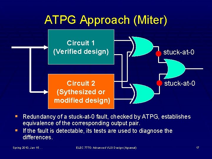
ATPG Approach (Miter) Circuit 1 (Verified design) Circuit 2 (Sythesized or modified design) stuck-at-0 § Redundancy of a stuck-at-0 fault, checked by ATPG, establishes § equivalence of the corresponding output pair. If the fault is detectable, its tests are used to diagnose the differences. Spring 2010, Jan 15. . ELEC 7770: Advanced VLSI Design (Agrawal) 17

Difficulties with Miter § ATPG is NP-complete. § When circuits are equivalent, proving § redundancy of faults is computationally expensive. When circuits are different, test vectors are quickly found, but diagnosis is difficult. Spring 2010, Jan 15. . ELEC 7770: Advanced VLSI Design (Agrawal) 18

A Heuristic Approach § Derive V 1, test vectors for all faults in C 1. § Derive V 2, test vectors for all faults in C 2. § If the combined set, V 1+V 2, produces the same § outputs from the two circuits, then they are probably equivalent. Reference: V. D. Agrawal, “Choice of Tests for Logic Verification and Equivalence Checking and the Use of Fault Simulation, ” Proc. 13 th International Conf. VLSI Design, January 2000, pp. 306 -311. Spring 2010, Jan 15. . ELEC 7770: Advanced VLSI Design (Agrawal) 19

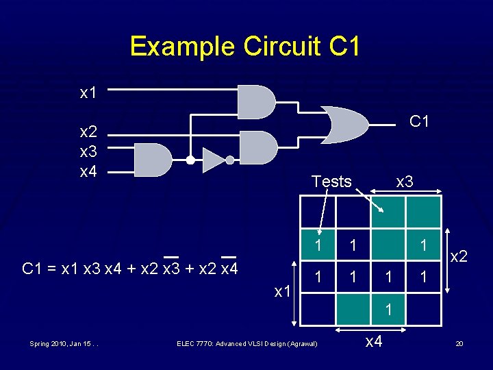
Example Circuit C 1 x 1 C 1 x 2 x 3 x 4 Tests C 1 = x 1 x 3 x 4 + x 2 x 3 + x 2 x 4 x 1 1 1 x 3 1 1 x 2 1 1 Spring 2010, Jan 15. . ELEC 7770: Advanced VLSI Design (Agrawal) x 4 20

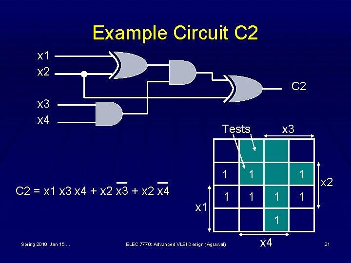
Example Circuit C 2 x 1 x 2 C 2 x 3 x 4 Tests C 2 = x 1 x 3 x 4 + x 2 x 3 + x 2 x 4 x 1 1 1 x 3 1 1 x 2 1 1 Spring 2010, Jan 15. . ELEC 7770: Advanced VLSI Design (Agrawal) x 4 21

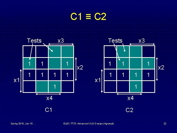
C 1 ≡ C 2 Tests x 1 1 1 x 3 Tests 1 1 1 x 2 x 1 1 1 x 3 1 1 1 Spring 2010, Jan 15. . x 2 1 1 x 4 C 1 C 2 ELEC 7770: Advanced VLSI Design (Agrawal) 22

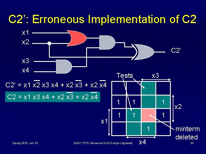
C 2’: Erroneous Implementation of C 2 x 1 x 2 C 2’ x 3 x 4 Tests x 3 C 2’ = x 1 x 2 x 3 x 4 + x 2 x 3 + x 2 x 4 C 2 = x 1 x 3 x 4 + x 2 x 3 + x 2 x 4 x 1 1 1 1 Spring 2010, Jan 15. . ELEC 7770: Advanced VLSI Design (Agrawal) x 4 x 2 minterm deleted 23

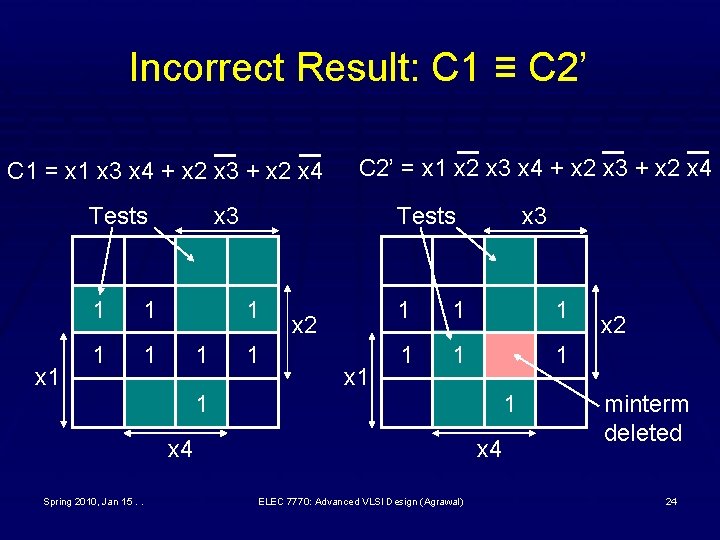
Incorrect Result: C 1 ≡ C 2’ C 1 = x 1 x 3 x 4 + x 2 x 3 + x 2 x 4 Tests x 1 1 1 C 2’ = x 1 x 2 x 3 x 4 + x 2 x 3 + x 2 x 4 x 3 Tests 1 1 1 x 2 x 1 x 3 1 1 1 1 x 4 Spring 2010, Jan 15. . x 4 ELEC 7770: Advanced VLSI Design (Agrawal) x 2 minterm deleted 24

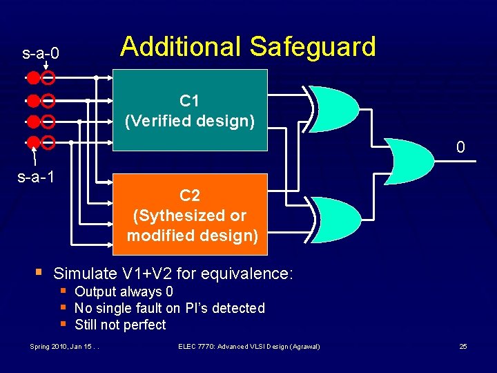
s-a-0 Additional Safeguard C 1 (Verified design) 0 s-a-1 C 2 (Sythesized or modified design) § Simulate V 1+V 2 for equivalence: § Output always 0 § No single fault on PI’s detected § Still not perfect Spring 2010, Jan 15. . ELEC 7770: Advanced VLSI Design (Agrawal) 25

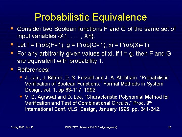
Probabilistic Equivalence § Consider two Boolean functions F and G of the same set of § § § input variables {X 1, . . . , Xn}. Let f = Prob(F=1), g = Prob(G=1), xi = Prob(Xi=1) For any arbitrarily given values of xi, if f = g, then F and G are equivalent with probability 1. References: § J. Jain, J. Bittner, D. S. Fussell and J. A. Abraham, “Probabilistic § Verification of Boolean Functions, ” Formal Methods in System Design, vol. 1, pp 63 -117, 1992. V. D. Agrawal and D. Lee, “Characteristic Polynomial Method for Verification and Test of Combinational Circuits, ” Proc. 9 th International Conf. VLSI Design, January 1996, pp. 341 -342. Spring 2010, Jan 15. . ELEC 7770: Advanced VLSI Design (Agrawal) 26

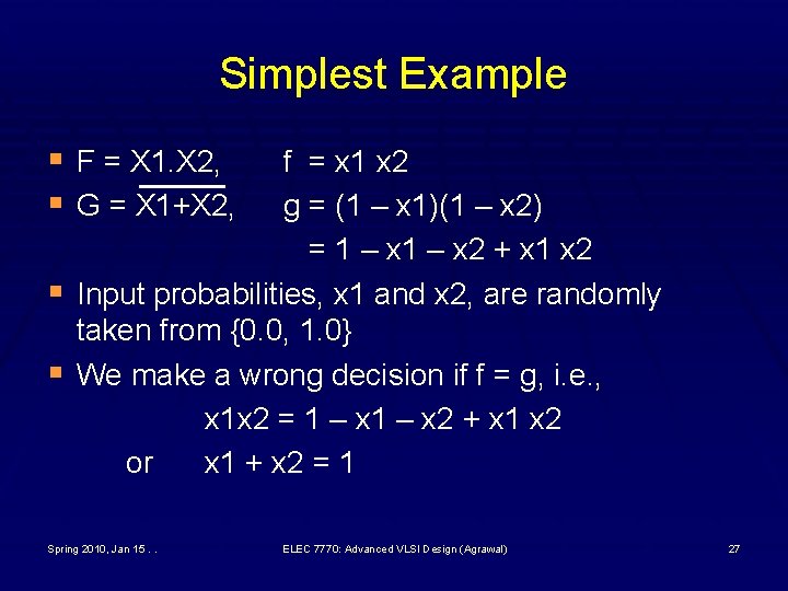
Simplest Example § F = X 1. X 2, § G = X 1+X 2, § § f = x 1 x 2 g = (1 – x 1)(1 – x 2) = 1 – x 2 + x 1 x 2 Input probabilities, x 1 and x 2, are randomly taken from {0. 0, 1. 0} We make a wrong decision if f = g, i. e. , x 1 x 2 = 1 – x 2 + x 1 x 2 or x 1 + x 2 = 1 Spring 2010, Jan 15. . ELEC 7770: Advanced VLSI Design (Agrawal) 27

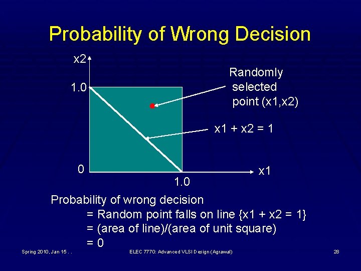
Probability of Wrong Decision x 2 Randomly selected point (x 1, x 2) 1. 0 x 1 + x 2 = 1 0 1. 0 x 1 Probability of wrong decision = Random point falls on line {x 1 + x 2 = 1} = (area of line)/(area of unit square) =0 Spring 2010, Jan 15. . ELEC 7770: Advanced VLSI Design (Agrawal) 28

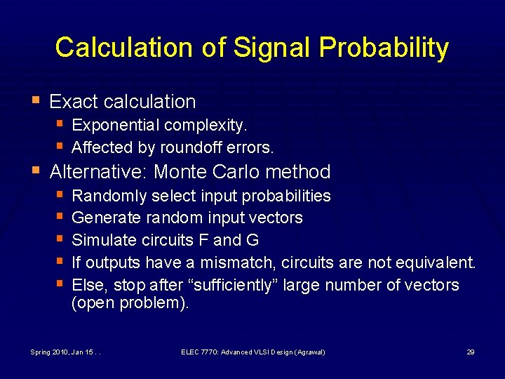
Calculation of Signal Probability § Exact calculation § Exponential complexity. § Affected by roundoff errors. § Alternative: Monte Carlo method § Randomly select input probabilities § Generate random input vectors § Simulate circuits F and G § If outputs have a mismatch, circuits are not equivalent. § Else, stop after “sufficiently” large number of vectors (open problem). Spring 2010, Jan 15. . ELEC 7770: Advanced VLSI Design (Agrawal) 29

References on Signal Probability § S. C. Seth and V. D. Agrawal, “A New Model for § Computation of Probabilistic Testability in Combinational Circuits, ” INTEGRATION, The VLSI Journal, vol. 7, pp. 49 -75, 1989. V. D. Agrawal and D. Lee and H. Woźniakowski, “Numerical Computation of Characteristic Polynomials of Boolean Functions and its Applications, ” Numerical Algorithms, vol. 17, pp. 261 -278, 1998. Spring 2010, Jan 15. . ELEC 7770: Advanced VLSI Design (Agrawal) 30

More on Equivalence Checking § Don’t cares § Sequential circuits § Time-frame expansion § Initial state § Design debugging (diagnosis) § Reference: S. -Y. Hwang and K. -T. Cheng, Formal Equivalence Checking and Design Debugging, Springer, 1998. Spring 2010, Jan 15. . ELEC 7770: Advanced VLSI Design (Agrawal) 31

Methods of Equivalence Checking § Satisfiability algorithms § ATPG methods § Binary decision diagrams (BDD) Spring 2010, Jan 15. . ELEC 7770: Advanced VLSI Design (Agrawal) 32

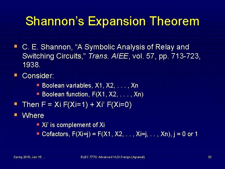
Shannon’s Expansion Theorem § C. E. Shannon, “A Symbolic Analysis of Relay and § § § Switching Circuits, ” Trans. AIEE, vol. 57, pp. 713 -723, 1938. Consider: § Boolean variables, X 1, X 2, . . . , Xn § Boolean function, F(X 1, X 2, . . . , Xn) Then F = Xi F(Xi=1) + Xi’ F(Xi=0) Where § Xi’ is complement of Xi § Cofactors, F(Xi=j) = F(X 1, X 2, . . , Xi=j, . . , Xn), j = 0 or 1 Spring 2010, Jan 15. . ELEC 7770: Advanced VLSI Design (Agrawal) 33

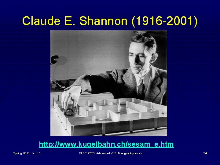
Claude E. Shannon (1916 -2001) http: //www. kugelbahn. ch/sesam_e. htm Spring 2010, Jan 15. . ELEC 7770: Advanced VLSI Design (Agrawal) 34

Shannon’s Legacy § A Symbolic Analysis of Relay and Switching Circuits, § § § Master’s Thesis, MIT, 1940. Perhaps the most influential master’s thesis of the 20 th century. An Algebra for Theoretical Genetics, Ph. D Thesis, MIT, 1940. Founded the field of Information Theory. C. E. Shannon and W. Weaver, The Mathematical Theory of Communication, University of Illinois Press, 1949. A “must read. ” Spring 2010, Jan 15. . ELEC 7770: Advanced VLSI Design (Agrawal) 35

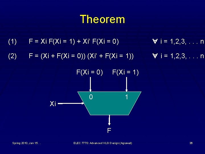
Theorem (1) F = Xi F(Xi = 1) + Xi’ F(Xi = 0) ∀ i = 1, 2, 3, . . . n (2) F = (Xi + F(Xi = 0)) (Xi’ + F(Xi = 1)) ∀ i = 1, 2, 3, . . . n Xi F(Xi = 0) F(Xi = 1) 0 1 F Spring 2010, Jan 15. . ELEC 7770: Advanced VLSI Design (Agrawal) 36

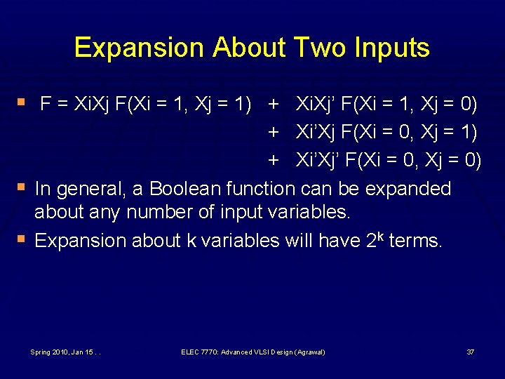
Expansion About Two Inputs § F = Xi. Xj F(Xi = 1, Xj = 1) + Xi. Xj’ F(Xi = 1, Xj = 0) § § + Xi’Xj F(Xi = 0, Xj = 1) + Xi’Xj’ F(Xi = 0, Xj = 0) In general, a Boolean function can be expanded about any number of input variables. Expansion about k variables will have 2 k terms. Spring 2010, Jan 15. . ELEC 7770: Advanced VLSI Design (Agrawal) 37

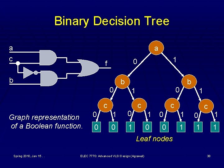
Binary Decision Tree a c a b 0 c Graph representation of a Boolean function. 1 0 f b 0 1 0 0 0 1 b c 1 0 0 0 c 1 0 1 1 Leaf nodes Spring 2010, Jan 15. . ELEC 7770: Advanced VLSI Design (Agrawal) 38

Binary Decision Diagrams § Binary decision diagram (BDD) is a graph representation § of a Boolean function, directly derivable from Shannon’s expansion. References: § C. Y. Lee, “Representation of Switching Circuits by Binary § Decision Diagrams, ” Bell Syst. Tech J. , vol. 38, pp. 985 -999, July 1959. S. Akers, “Binary Decision Diagrams, ” IEEE Trans. Computers, vol. C-27, no. 6, pp. 509 -516, June 1978. § Ordered BDD (OBDD) and Reduced Order BDD § (ROBDD). Reference: § R. E. Bryant, “Graph-Based Algorithms for Boolean Function Manipulation, ” IEEE Trans. Computers, vol. C-35, no. 8, pp. 677691, August 1986. Spring 2010, Jan 15. . ELEC 7770: Advanced VLSI Design (Agrawal) 39

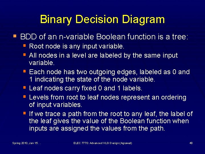
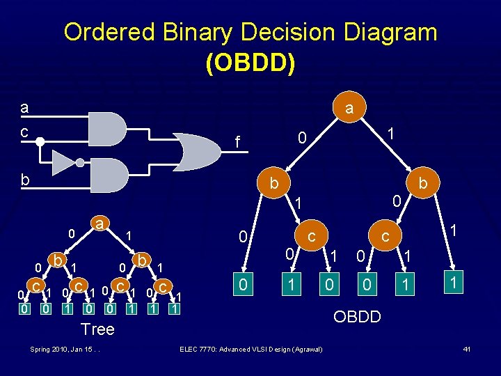
Binary Decision Diagram § BDD of an n-variable Boolean function is a tree: § Root node is any input variable. § All nodes in a level are labeled by the same input § § variable. Each node has two outgoing edges, labeled as 0 and 1 indicating the state of the node variable. Leaf nodes carry fixed 0 and 1 labels. Levels from root to leaf nodes represent an ordering of input variables. If we trace a path from the root to any leaf, the label of the leaf gives the value of the Boolean function when inputs are assigned the values from the path. Spring 2010, Jan 15. . ELEC 7770: Advanced VLSI Design (Agrawal) 40

Ordered Binary Decision Diagram (OBDD) a c a b 1 0 f b 0 1 0 b 0 0 0 a 1 0 c 1 0 1 b 1 0 c 1 0 0 1 1 1 0 0 c 1 Tree Spring 2010, Jan 15. . b ELEC 7770: Advanced VLSI Design (Agrawal) 1 c 1 0 0 0 1 1 1 OBDD 41

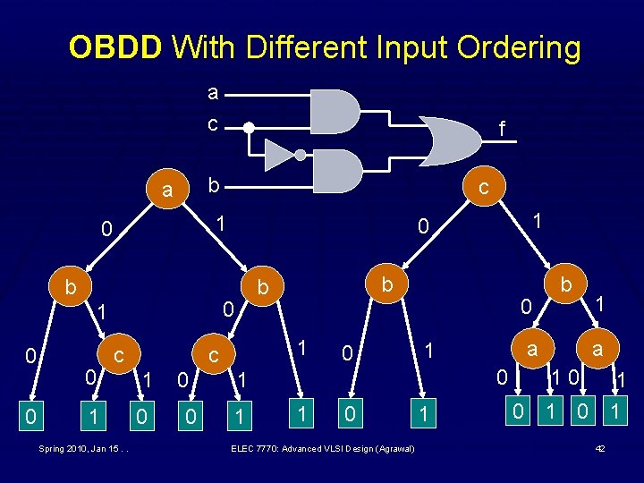
OBDD With Different Input Ordering a c b a b 0 c 1 Spring 2010, Jan 15. . 0 0 0 b b 1 c 1 1 0 0 1 0 c 1 0 0 f 0 0 1 a 1 0 1 1 0 ELEC 7770: Advanced VLSI Design (Agrawal) 1 b 1 a 10 1 0 1 42

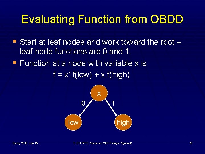
Evaluating Function from OBDD § Start at leaf nodes and work toward the root – § leaf node functions are 0 and 1. Function at a node with variable x is f = x’. f(low) + x. f(high) x 0 low Spring 2010, Jan 15. . 1 high ELEC 7770: Advanced VLSI Design (Agrawal) 43

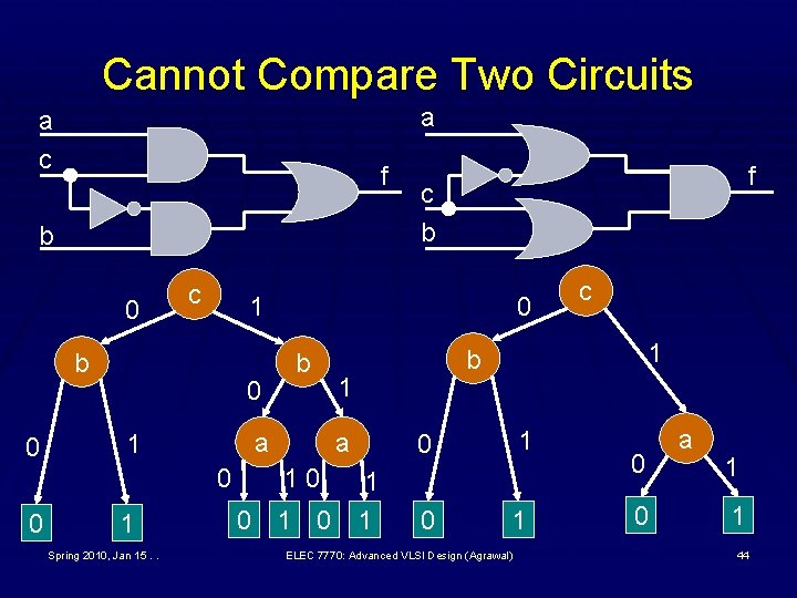
Cannot Compare Two Circuits a a c f b 0 c 0 1 Spring 2010, Jan 15. . 0 b a 1 0 0 c b 1 b 0 f 1 b 1 a 0 1 10 1 0 1 c ELEC 7770: Advanced VLSI Design (Agrawal) 0 0 a 1 1 44

OBDD Graph Isomorphism § Two OBDDs are isomorphic if there is one-to§ § § one mapping between the vertex sets with respect to adjacency, labels and leaf values. Two isomorphic OBDDs represent the same function. Two identical circuits may not have identical OBDDs even when same variable ordering is used. Comparison is possible if: § Same variable ordering is used. § Any redundancies in graphs are removed. Spring 2010, Jan 15. . ELEC 7770: Advanced VLSI Design (Agrawal) 45

Reduced Ordered BDD (ROBDD) § Directed acyclic graph (DAG) (*). § Contains just two leaf nodes labeled 0 and 1. § Variables are indexed, 1, 2, . . . n, such that the § § index of a node is greater than that of its child (*). A node has exactly two child nodes, low and high such that low ≠ high. Graph contains no pair of nodes such that subgraphs rooted in them are isomorphic. * Properties common to OBDD. Spring 2010, Jan 15. . ELEC 7770: Advanced VLSI Design (Agrawal) 46

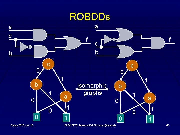
ROBDDs a a c f b 0 0 c 1 1 0 Spring 2010, Jan 15. . c b 0 f 0 a Isomorphic graphs 1 b 1 0 1 1 ELEC 7770: Advanced VLSI Design (Agrawal) 0 0 a 1 1 47

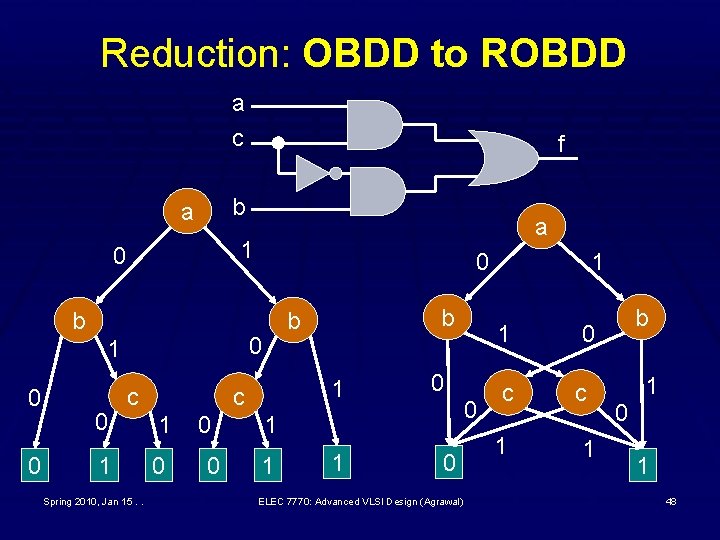
Reduction: OBDD to ROBDD a c b a b 0 0 c 1 Spring 2010, Jan 15. . 1 c 1 0 0 0 b b 0 1 0 a 1 0 0 f 0 0 1 1 1 0 ELEC 7770: Advanced VLSI Design (Agrawal) 1 1 0 c c 1 1 b 1 0 1 48

Properties of ROBDD § Unique for given variable ordering – graph isomorphism § § § verifies logic equivalence. Size (number of nodes) changes with variable ordering – worst-case size is exponential (e. g. , integer multiplier). Other applications: logic synthesis, testing. For algorithms to derive ROBDD, see § R. E. Bryant, “Graph-Based Algorithms for Boolean Function § § Manipulation, ” IEEE Trans. Computers, vol. C-35, no. 8, pp. 677691, August 1986. G. De Micheli, Synthesis and Optimization of Digital Circuits, New York: Mc. Graw-Hill, 1994. S. Devadas, A. Ghosh, and K. Keutzer, Logic Synthesis, New York: Mc. Graw-Hill, 1994. Spring 2010, Jan 15. . ELEC 7770: Advanced VLSI Design (Agrawal) 49