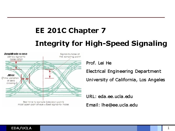
EE 201 C Chapter 7 Integrity for HighSpeed
![High-speed Links are Everywhere Backbone Router Rack PC or Console EDA/UCLA [Sredojevic: ICCAD’ 08] High-speed Links are Everywhere Backbone Router Rack PC or Console EDA/UCLA [Sredojevic: ICCAD’ 08]](https://slidetodoc.com/presentation_image_h/f21aec432f28f4a55316c53f83be3e94/image-2.jpg)
- Slides: 38

EE 201 C Chapter 7 Integrity for High-Speed Signaling Prof. Lei He Electrical Engineering Department University of California, Los Angeles URL: eda. ee. ucla. edu Email: lhe@ee. ucla. edu EDA/UCLA 1
![Highspeed Links are Everywhere Backbone Router Rack PC or Console EDAUCLA Sredojevic ICCAD 08 High-speed Links are Everywhere Backbone Router Rack PC or Console EDA/UCLA [Sredojevic: ICCAD’ 08]](https://slidetodoc.com/presentation_image_h/f21aec432f28f4a55316c53f83be3e94/image-2.jpg)
High-speed Links are Everywhere Backbone Router Rack PC or Console EDA/UCLA [Sredojevic: ICCAD’ 08] 2

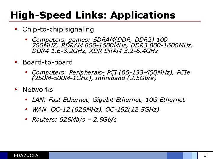
High-Speed Links: Applications • Chip-to-chip signaling • Computers, games: SDRAM(DDR, DDR 2) 100 - 700 MHZ, RDRAM 800 -1600 MHz, DDR 3 800 -1600 MHz, DDR 4 1. 6 -3. 2 GHz, XDR DRAM 3. 2 -6. 4 GHz • Board-to-board • Computers: Peripherals- PCI (66 -133 -400 MHz), PCIe (250 M-500 M-1 GHz), Infiniband (2. 5 Gb/s) • Networks • LAN: Fast Ethernet, Gigabit Ethernet, 10 G Ethernet • WAN: OC-12 (625 MHz), OC-192(12. 5 GHz) • Routers: 625 Mb/s – 2. 5 Gb/s EDA/UCLA 3

Outline • Link Design Basics • Signal Integrity • High Speed Signaling Architectures • Equalization EDA/UCLA 4

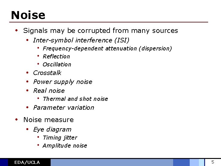
Noise • Signals may be corrupted from many sources • Inter-symbol interference (ISI) • Frequency-dependent attenuation (dispersion) • Reflection • Oscillation • Crosstalk • Power supply noise • Real noise • Thermal and shot noise • Parameter variation • Noise measure • Eye diagram • Timing jitter • Amplitude noise EDA/UCLA 5

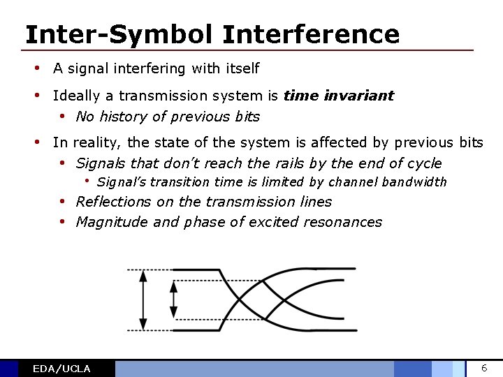
Inter-Symbol Interference • A signal interfering with itself • Ideally a transmission system is time invariant • No history of previous bits • In reality, the state of the system is affected by previous bits • Signals that don’t reach the rails by the end of cycle • Signal’s transition time is limited by channel bandwidth • Reflections on the transmission lines • Magnitude and phase of excited resonances EDA/UCLA 6

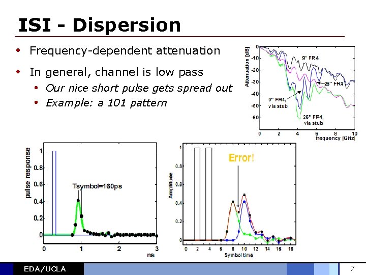
ISI - Dispersion • Frequency-dependent attenuation • In general, channel is low pass • Our nice short pulse gets spread out • Example: a 101 pattern EDA/UCLA 7

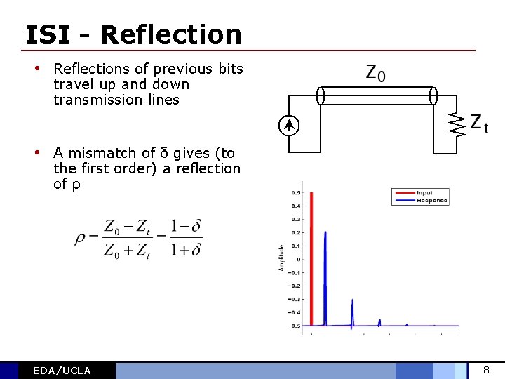
ISI - Reflection • Reflections of previous bits travel up and down transmission lines • A mismatch of δ gives (to the first order) a reflection of ρ EDA/UCLA 8

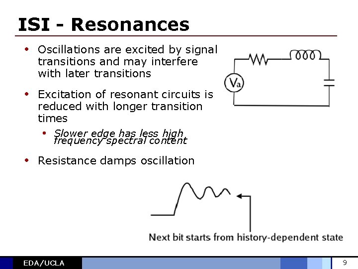
ISI - Resonances • Oscillations are excited by signal transitions and may interfere with later transitions • Excitation of resonant circuits is reduced with longer transition times • Slower edge has less high frequency spectral content • Resistance damps oscillation EDA/UCLA 9

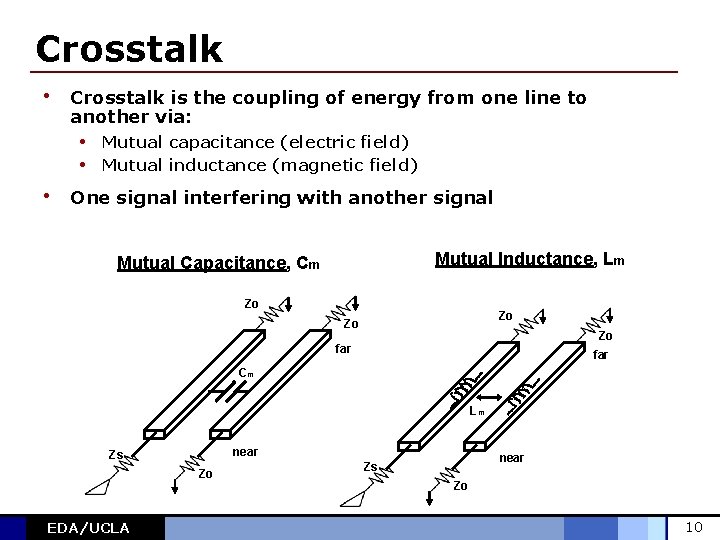
Crosstalk • Crosstalk is the coupling of energy from one line to another via: • Mutual capacitance (electric field) • Mutual inductance (magnetic field) • One signal interfering with another signal Mutual Inductance, Lm Mutual Capacitance, Cm Zo Zo far Cm Lm near Zs Zo EDA/UCLA near Zs Zo 10

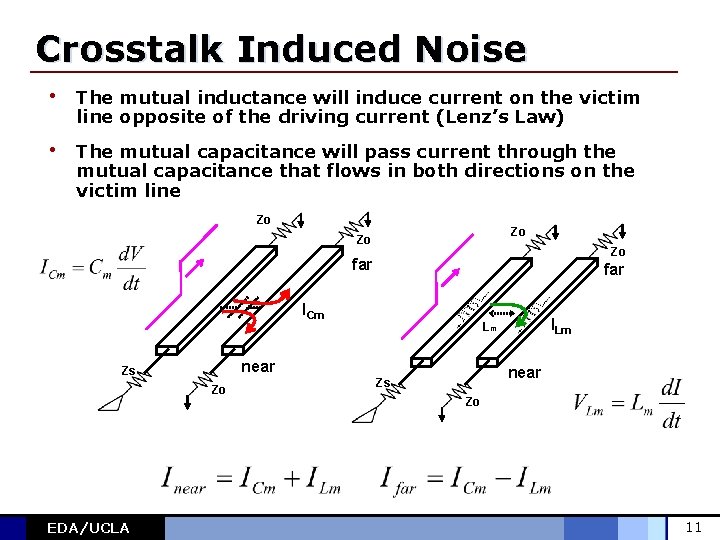
Crosstalk Induced Noise • The mutual inductance will induce current on the victim line opposite of the driving current (Lenz’s Law) • The mutual capacitance will pass current through the mutual capacitance that flows in both directions on the victim line Zo Zo far ICm near Zs Zo EDA/UCLA ILm Lm near Zs Zo 11

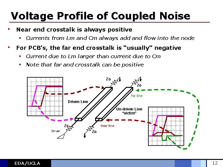
Voltage Profile of Coupled Noise • Near end crosstalk is always positive • Currents from Lm and Cm always add and flow into the node • For PCB’s, the far end crosstalk is “usually” negative • Current due to Lm larger than current due to Cm • Note that far and crosstalk can be positive Zo Zo Far End Driven Line Un-driven Line “victim” Zs Driver EDA/UCLA Near End Zo 12

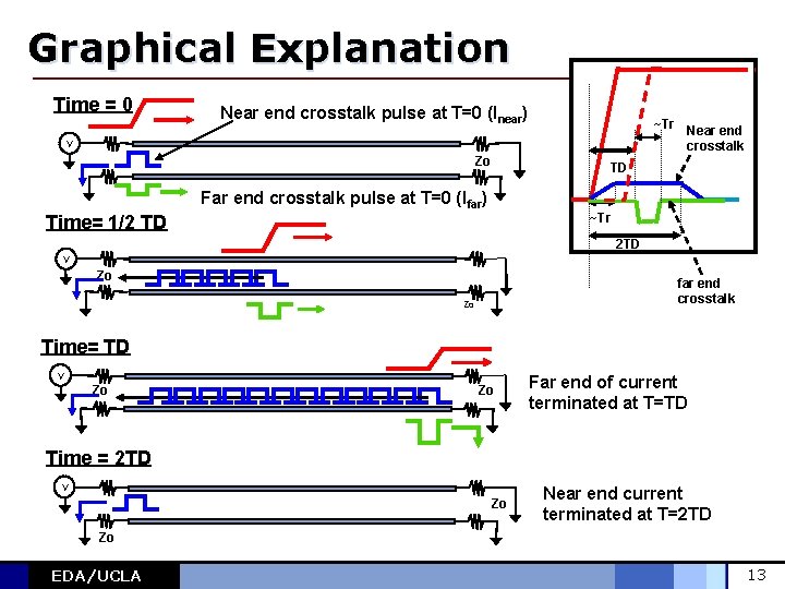
Graphical Explanation Time = 0 Near end crosstalk pulse at T=0 (Inear) ~Tr V Zo Time= 1/2 TD Near end crosstalk TD Far end crosstalk pulse at T=0 (Ifar) ~Tr 2 TD V Zo far end crosstalk Zo Time= TD V Zo Zo Far end of current terminated at T=TD Time = 2 TD V Zo Near end current terminated at T=2 TD Zo EDA/UCLA 13

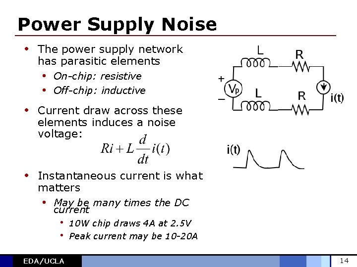
Power Supply Noise • The power supply network has parasitic elements • On-chip: resistive • Off-chip: inductive • Current draw across these elements induces a noise voltage: • Instantaneous current is what matters • May be many times the DC current • 10 W chip draws 4 A at 2. 5 V • Peak current may be 10 -20 A EDA/UCLA 14

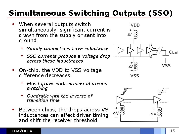
Simultaneous Switching Outputs (SSO) • When several outputs switch simultaneously, significant current is drawn from the supply or sent into ground • Supply connections have inductance • SSO currents produce a voltage drop across these inductances • On-chip, the VDD to VSS voltage difference decreases • Effect grows with number of drivers switching • Quadratic with the inverse of transition time • Between chips, the drops across VSS inductances can effect driver timing and shift the receiver threshold EDA/UCLA 15

Other Noise Sources • Alpha particles • 5 Me. V particle injects 730 f. C of charge into substrate • One node typically collects less than 50 f. C • Thermal and shot noise • Proportional to bandwidth – typically in the u. V • Parameter mismatch • VT and β have deviation proportional to 1/sqrt(WL) • Systematic variations depend on layout EDA/UCLA 16

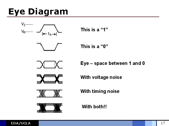
Eye Diagram This is a “ 1” This is a “ 0” Eye – space between 1 and 0 With voltage noise With timing noise With both!! EDA/UCLA 17

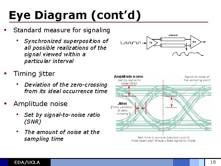
Eye Diagram (cont’d) • Standard measure for signaling • Synchronized superposition of all possible realizations of the signal viewed within a particular interval • Timing jitter • Deviation of the zero-crossing from its ideal occurrence time • Amplitude noise • Set by signal-to-noise ratio (SNR) • The amount of noise at the sampling time EDA/UCLA 18

Outline • Link Design Basics • Signal Integrity • High Speed Signaling Architectures • Equalization EDA/UCLA 19

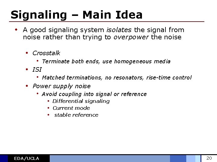
Signaling – Main Idea • A good signaling system isolates the signal from noise rather than trying to overpower the noise • Crosstalk • Terminate both ends, use homogeneous media • ISI • Matched terminations, no resonators, rise-time control • Power supply noise • Avoid coupling into signal or reference • Differential signaling • Current mode • stable reference EDA/UCLA 20

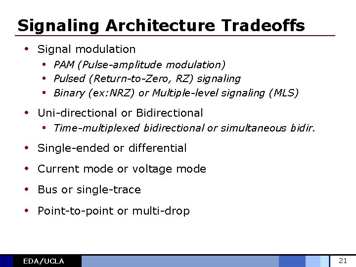
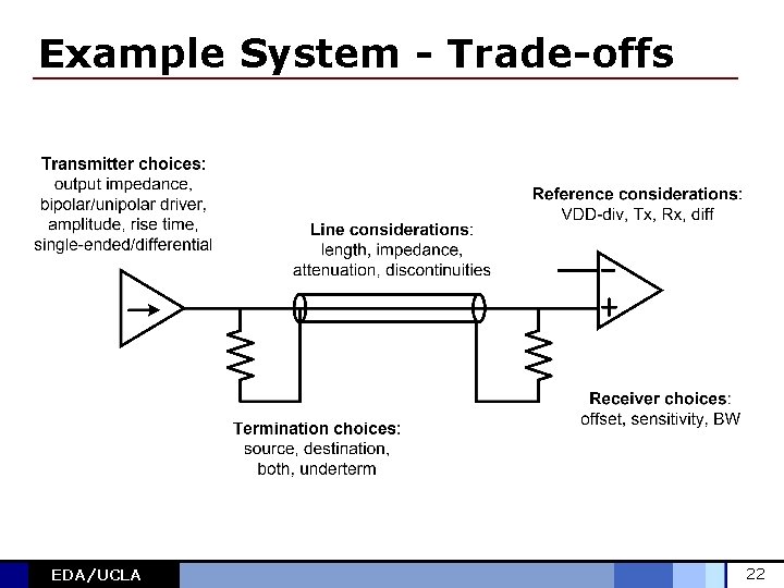
Signaling Architecture Tradeoffs • Signal modulation • PAM (Pulse-amplitude modulation) • Pulsed (Return-to-Zero, RZ) signaling • Binary (ex: NRZ) or Multiple-level signaling (MLS) • Uni-directional or Bidirectional • Time-multiplexed bidirectional or simultaneous bidir. • Single-ended or differential • Current mode or voltage mode • Bus or single-trace • Point-to-point or multi-drop EDA/UCLA 21

Example System - Trade-offs EDA/UCLA 22

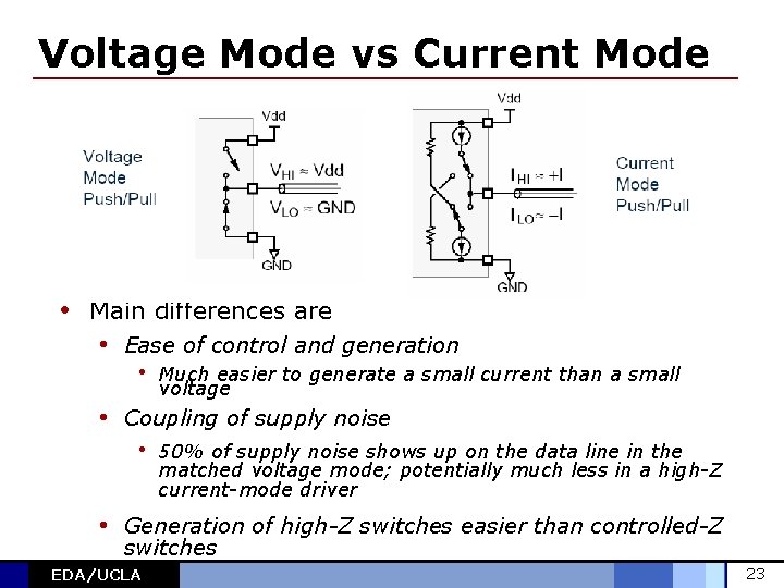
Voltage Mode vs Current Mode • Main differences are • Ease of control and generation • Much easier to generate a small current than a small voltage • Coupling of supply noise • 50% of supply noise shows up on the data line in the matched voltage mode; potentially much less in a high-Z current-mode driver • Generation of high-Z switches easier than controlled-Z switches EDA/UCLA 23

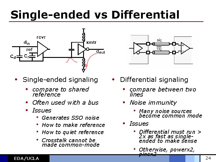
Single-ended vs Differential • Single-ended signaling • Differential signaling • compare to shared • compare between two • • • reference Often used with a bus Issues • • EDA/UCLA Generates SSO noise How to make reference How to quiet reference Crosstalk cannot be made common-mode lines Noise immunity • Many noise sources become common mode • Issues • Differential must run > 2 x as fast as singleended to make sense • Otherwise, powerx 2, pinsx 2 24

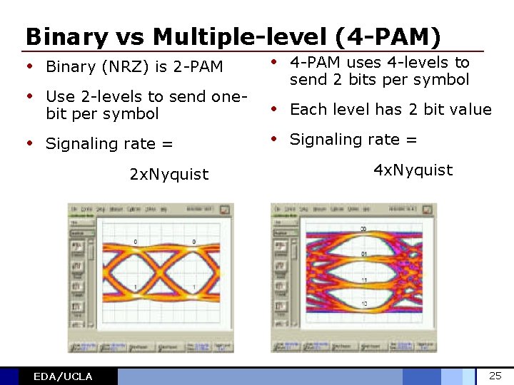
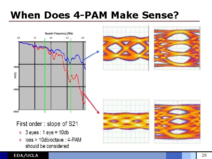
Binary vs Multiple-level (4 -PAM) • Binary (NRZ) is 2 -PAM • Use 2 -levels to send onebit per symbol • Signaling rate = 2 x. Nyquist EDA/UCLA • 4 -PAM uses 4 -levels to send 2 bits per symbol • Each level has 2 bit value • Signaling rate = 4 x. Nyquist 25

When Does 4 -PAM Make Sense? EDA/UCLA 26

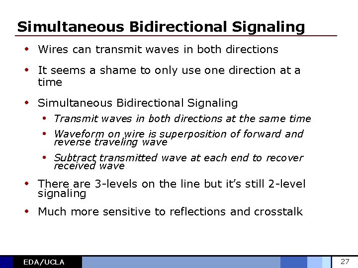
Simultaneous Bidirectional Signaling • Wires can transmit waves in both directions • It seems a shame to only use one direction at a time • Simultaneous Bidirectional Signaling • Transmit waves in both directions at the same time • Waveform on wire is superposition of forward and reverse traveling wave • Subtract transmitted wave at each end to recover received wave • There are 3 -levels on the line but it’s still 2 -level signaling • Much more sensitive to reflections and crosstalk EDA/UCLA 27

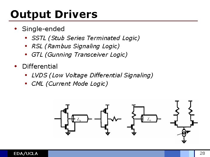
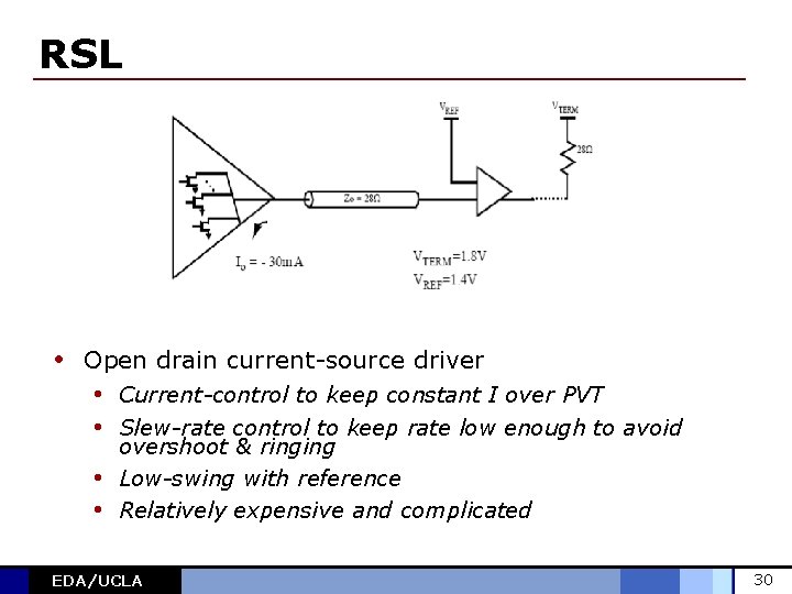
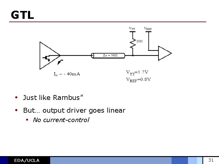
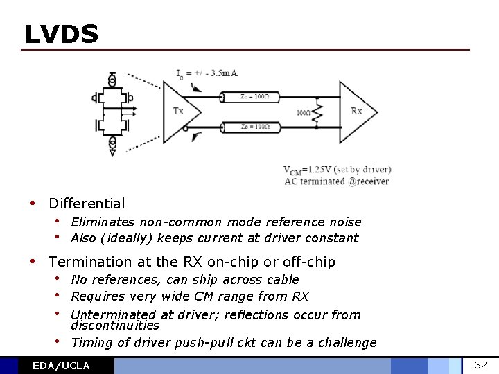
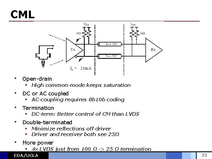
Output Drivers • Single-ended • SSTL (Stub Series Terminated Logic) • RSL (Rambus Signaling Logic) • GTL (Gunning Transceiver Logic) • Differential • LVDS (Low Voltage Differential Signaling) • CML (Current Mode Logic) EDA/UCLA 28

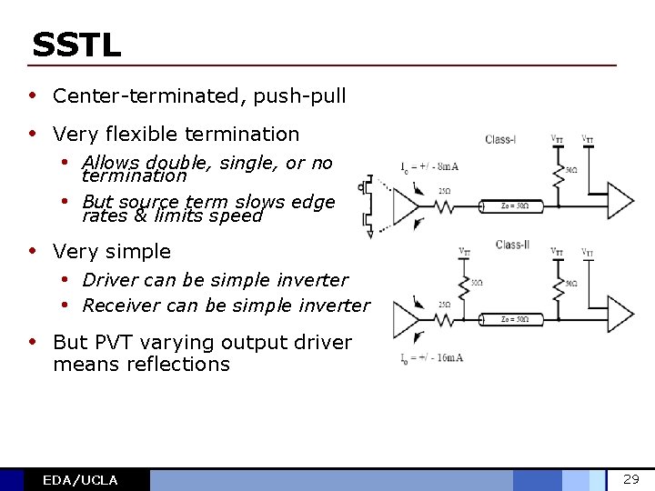
SSTL • Center-terminated, push-pull • Very flexible termination • Allows double, single, or no • termination But source term slows edge rates & limits speed • Very simple • Driver can be simple inverter • Receiver can be simple inverter • But PVT varying output driver means reflections EDA/UCLA 29

RSL • Open drain current-source driver • Current-control to keep constant I over PVT • Slew-rate control to keep rate low enough to avoid • • overshoot & ringing Low-swing with reference Relatively expensive and complicated EDA/UCLA 30

GTL • Just like Rambus” • But… output driver goes linear • No current-control EDA/UCLA 31

LVDS • Differential • Eliminates non-common mode reference noise • Also (ideally) keeps current at driver constant • Termination at the RX on-chip or off-chip • No references, can ship across cable • Requires very wide CM range from RX • Unterminated at driver; reflections occur from • discontinuities Timing of driver push-pull ckt can be a challenge EDA/UCLA 32

CML • Open-drain • High common-mode keeps saturation • DC or AC coupled • AC-coupling requires 8 b 10 b coding • Termination • DC-term: Better control of CM than LVDS • Double-terminated • Minimize reflections off driver • Driver and receiver both see 25Ω • More power • 4 x LVDS just from 100 Ω -> 25 Ω termination EDA/UCLA 33

Outline • Link Design Basics • Signal Integrity • High Speed Signaling Architectures • Equalization EDA/UCLA 34

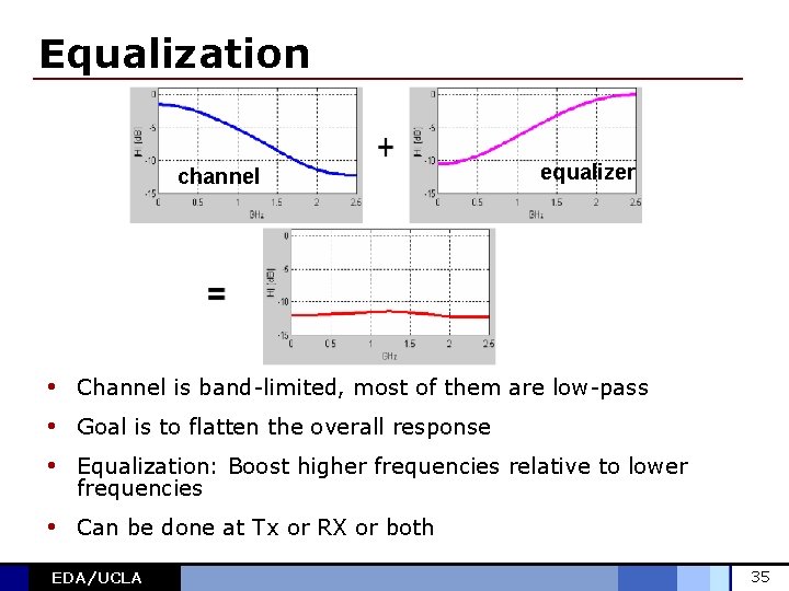
Equalization channel equalizer • Channel is band-limited, most of them are low-pass • Goal is to flatten the overall response • Equalization: Boost higher frequencies relative to lower frequencies • Can be done at Tx or RX or both EDA/UCLA 35

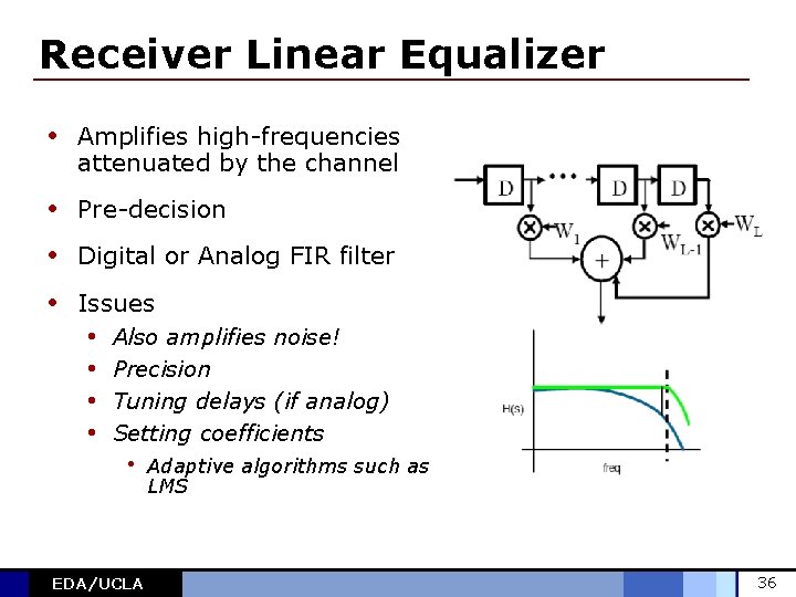
Receiver Linear Equalizer • Amplifies high-frequencies attenuated by the channel • Pre-decision • Digital or Analog FIR filter • Issues • • Also amplifies noise! Precision Tuning delays (if analog) Setting coefficients • Adaptive algorithms such as LMS EDA/UCLA 36

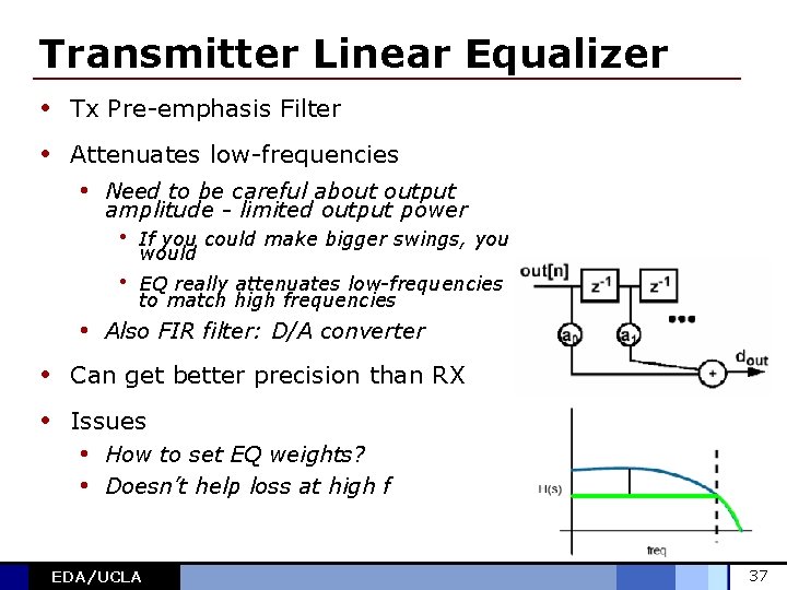
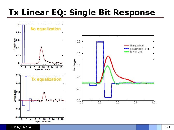
Transmitter Linear Equalizer • Tx Pre-emphasis Filter • Attenuates low-frequencies • Need to be careful about output amplitude - limited output power • If you could make bigger swings, you would • EQ really attenuates low-frequencies to match high frequencies • Also FIR filter: D/A converter • Can get better precision than RX • Issues • How to set EQ weights? • Doesn’t help loss at high f EDA/UCLA 37

Tx Linear EQ: Single Bit Response EDA/UCLA 38