ECE 545 Lecture 12 Design of Controllers using
 Charts George")


 Control & Status")


 Charts ECE 448 – FPGA and ASIC Design with VHDL")


 State name Output signals or actions (Moore type)")


 Inputs Next State function Next State clock reset concurrent statements")
 USE ieee. std_logic_1164. all ; ENTITY simple IS PORT")
 CASE y IS WHEN A => IF w =")
 END IF ; END PROCESS ; z <= '1'")


 Inputs Next State function Next State clock reset concurrent statements")
 LIBRARY ieee ; USE ieee. std_logic_1164. all ; ENTITY")
 CASE y IS WHEN A => IF w =")
 END IF ; END PROCESS ; z <= '1'")
 reset g 1 r 2 Arbiter g 2 g")
 000 Reset Idle 0 -- 1 -- gnt 1")
 35")

 Inputs Next State function Next State clock reset concurrent statements")
 LIBRARY ieee; USE ieee. std_logic_1164. all; ENTITY arbiter IS")
 BEGIN PROCESS ( Resetn, Clock ) BEGIN IF Resetn")
 WHEN gnt 3 => IF r(3) = '0' THEN")


 decision boxes: with")


 k: log 2(w) (constant) A,")


![Protocol (1) An external circuit first loads all round keys S[0], S[1], S[2], …,](https://slidetodoc.com/presentation_image_h/3728bf782063c7b97334e7ea1f340c2e/image-60.jpg "Protocol (1) An external circuit first loads all round keys S[0], S[1], S[2], …,")
 When the encryption is completed, signal DONE becomes active, and the output")


 Inputs Next State function Next State clock reset Present")
 Inputs Next State function Next State clock")


 Process(clk, reset) 83")


- Slides: 87
ECE 545 Lecture 12 Design of Controllers using Algorithmic State Machine (ASM) Charts George Mason University
Required reading • P. Chu, RTL Hardware Design using VHDL Chapter 11, Register Transfer Methodology: Principle 2
Recommended reading • P. Chu, RTL Hardware Design using VHDL Chapter 12, Register Transfer Methodology: Practice 3
Slides based partially on • S. Brown and Z. Vranesic, Fundamentals of Digital Logic with VHDL Design Chapter 8, Synchronous Sequential Circuits Sections 8. 1 -8. 5 Chapter 8. 10, Algorithmic State Machine (ASM) Charts Chapter 10. 2 Design Examples 4
Structure of a Typical Digital System Data Inputs Datapath (Execution Unit) Control & Status Inputs Control Signals Controller (Control Unit) Status Signals Data Outputs Control & Status Outputs
Hardware Design with RTL VHDL Pseudocode Datapath Interface Controller Block diagram VHDL code ASM chart VHDL code
Steps of the Design Process Introduced in Class Today 1. 2. 3. 4. 5. Text description Interface Pseudocode Block diagram of the Datapath Interface with the division into Datapath and Controller 6. ASM chart of the Controller 7. RTL VHDL code of the Datapath, Controller, and Top-Level Unit 8. Testbench of the Datapath, Controller, and Top-Level Unit 9. Functional simulation and debugging 10. Synthesis and post-synthesis simulation 11. Implementation and timing simulation 12. Experimental testing
Generalized FSM Based on RTL Hardware Design by P. Chu 8
Generalized FSM Inputs Next State function Next State clock reset Present State Register Mealy Output function Moore Output function Mealy Outputs Moore Outputs Present State 9
Algorithmic State Machine (ASM) Charts ECE 448 – FPGA and ASIC Design with VHDL 10
Algorithmic State Machine – representation of a Finite State Machine suitable for FSMs with a larger number of inputs and outputs compared to FSMs expressed using state diagrams and state tables. 11
ASM Chart – Flowchart-like diagram – Provides the same info as a state diagram – More descriptive, better for complex description 12
Elements used in ASM charts (1) State name Output signals or actions (Moore type) 0 (False) (a) State box Condition expression 1 (True) (b) Decision box Conditional outputs or actions (Mealy type) (c) Conditional output box 13
State Box • State box – represents a state. • Equivalent to a node in a state diagram or a row in a state table. • Contains register transfer actions or output signals • Moore-type outputs are listed inside of the box. • It is customary to write only the name of the signal that has to be asserted in the given state, e. g. , z instead of z<=1. • Also, it might be useful to write an action to be taken, e. g. , count <= count + 1, and only later translate it to asserting a control signal that causes a given action to take place (e. g. , enable signal of a counter). State name Output signals or actions (Moore type) 14
Decision Box • Decision box – indicates that a given condition is to be tested and the exit path is to be chosen accordingly. The condition expression may include one or more inputs to the FSM. 0 (False) Condition expression 1 (True) 15
Conditional Output Box • Conditional output box • Denotes output signals that are of the Mealy type. • The condition that determines whether such outputs are generated is specified in the decision box. Conditional outputs or actions (Mealy type) 16
Counting: Block diagram + ASM ECE 448 – FPGA and ASIC Design with VHDL 17
Counting: Timing waveforms ECE 448 – FPGA and ASIC Design with VHDL 18
ASMs representing simple FSMs • Algorithmic state machines can model both Mealy and Moore Finite State Machines • They can also model machines that are of the mixed type 19
Moore FSM – Example 1: State diagram Reset w = 1 w = 0 A¤z=0 B¤z= 0 w = 1 w = 0 C¤z = 1 w = 1 20
Moore FSM – Example 1: State table Next state Present state w = 0 w = 1 A B C A A A B C C Output z 0 0 1 21
ASM Chart for Moore FSM – Example 2 22
Moore FSM process(clock, reset) Inputs Next State function Next State clock reset concurrent statements Present State Register Present State Output function Outputs 23
Example 1: VHDL code (1) USE ieee. std_logic_1164. all ; ENTITY simple IS PORT ( clock resetn w z END simple ; : IN STD_LOGIC ; : OUT STD_LOGIC ) ; ARCHITECTURE Behavior OF simple IS TYPE State_type IS (A, B, C) ; SIGNAL y : State_type ; BEGIN PROCESS ( resetn, clock ) BEGIN IF resetn = '0' THEN y <= A ; ELSIF rising_edge(clock) THEN 24
Example 1: VHDL code (2) CASE y IS WHEN A => IF w = ‘ 1' THEN y <= B ; ELSE y <= A ; END IF ; WHEN B => IF w = ‘ 1' THEN y <= C ; ELSE y <= A ; END IF ; WHEN C => IF w = '0' THEN y <= A ; ELSE y <= C ; END IF ; END CASE ; 25
Example 1: VHDL code (3) END IF ; END PROCESS ; z <= '1' WHEN y = C ELSE '0' ; END Behavior ; 26
Mealy FSM – Example 2: State diagram Reset w = 1¤z= 0 w = 0¤z= 0 A B w = 1¤z= 1 w = 0¤z= 0 27
ASM Chart for Mealy FSM – Example 2 28
Mealy FSM process(clock, reset) Inputs Next State function Next State clock reset concurrent statements Present State Register Output function Outputs 29
Example 3: VHDL code (1) LIBRARY ieee ; USE ieee. std_logic_1164. all ; ENTITY Mealy IS PORT ( clock : IN resetn : IN w : IN z : OUT END Mealy ; STD_LOGIC ; STD_LOGIC ) ; ARCHITECTURE Behavior OF Mealy IS TYPE State_type IS (A, B) ; SIGNAL y : State_type ; BEGIN PROCESS ( resetn, clock ) BEGIN IF resetn = '0' THEN y <= A ; ELSIF rising_edge(clock) THEN 30
Example 3: VHDL code (2) CASE y IS WHEN A => IF w = ‘ 1' THEN y <= B ; ELSE y <= A ; END IF ; WHEN B => IF w = '0' THEN y <= A ; ELSE y <= B ; END IF ; END CASE ; 31
Example 3: VHDL code (3) END IF ; END PROCESS ; z <= '1' WHEN (y = B) AND (w=‘ 1’) ELSE '0' ; END Behavior ; 32
Control Unit Example: Arbiter (1) reset g 1 r 2 Arbiter g 2 g 3 r 3 clock 33
Control Unit Example: Arbiter (2) 000 Reset Idle 0 -- 1 -- gnt 1 ¤ g 1 = 1 -0 - 1 -- 01 - gnt 2 ¤ g 2 = 1 --0 -1 - 001 gnt 3 ¤ g 3 = 1 --1 34
Control Unit Example: Arbiter (3) 35
ASM Chart for Control Unit - Example 4 36
Moore FSM process(clock, reset) Inputs Next State function Next State clock reset concurrent statements Present State Register Present State Output function Outputs 37
Example 4: VHDL code (1) LIBRARY ieee; USE ieee. std_logic_1164. all; ENTITY arbiter IS PORT ( Clock, Resetn r g END arbiter ; : IN : OUT STD_LOGIC ; STD_LOGIC_VECTOR(1 TO 3) ) ; ARCHITECTURE Behavior OF arbiter IS TYPE State_type IS (Idle, gnt 1, gnt 2, gnt 3) ; SIGNAL y : State_type ; 38
Example 4: VHDL code (2) BEGIN PROCESS ( Resetn, Clock ) BEGIN IF Resetn = '0' THEN y <= Idle ; ELSIF rising_edge(Clock) THEN CASE y IS WHEN Idle => IF r(1) = '1' THEN y <= gnt 1 ; ELSIF r(2) = '1' THEN y <= gnt 2 ; ELSIF r(3) = '1' THEN y <= gnt 3 ; ELSE y <= Idle ; END IF ; WHEN gnt 1 => IF r(1) = '0' THEN y <= Idle ; ELSE y <= gnt 1 ; END IF ; WHEN gnt 2 => IF r(2) = '0' THEN y <= Idle ; ELSE y <= gnt 2 ; END IF ; 39
Example 4: VHDL code (3) WHEN gnt 3 => IF r(3) = '0' THEN y <= Idle ; ELSE y <= gnt 3 ; END IF ; END CASE ; END IF ; END PROCESS ; g(1) <= '1' WHEN y = gnt 1 ELSE '0' ; g(2) <= '1' WHEN y = gnt 2 ELSE '0' ; g(3) <= '1' WHEN y = gnt 3 ELSE '0' ; END Behavior ; 40
Exercise Assuming ASM chart given on the next slide, supplement timing waveforms given in the answer sheet with the correct values of signals State, g 1, g 2, g 3, in the interval from 0 to 575 ns.
ASM Chart 42
Reset Clk r 1 r 2 r 3 State g 1 g 2 g 3 0 ns 100 ns 200 ns 300 ns 400 ns 500 ns
ASM Block • One state box • One or more (optional) decision boxes: with T (1) or F (0) exit paths • One or more (optional) conditional output boxes: for Mealy outputs 44
ASM Chart Rules • Difference between a regular flowchart and an ASM chart: – Transition governed by clock – Transition occurs between ASM blocks • Basic rules: – For a given input combination, there is one unique exit path from the current ASM block – Any closed loop in an ASM chart must include a state box Based on RTL Hardware Design by P. Chu 45
Incorrect ASM Charts Based on RTL Hardware Design by P. Chu 46
Class Exercise 1 STATISTICS
Pseudocode no_1 = no_2 = no_3 = sum = 0 for i=0 to k-1 do sum = sum + din if din > no_1 then no_3 = no_2 = no_1 = din elseif (din > no_2) then no_3 = no_2 = din elseif (din > no_3) then no_3 = din end if end for avr = sum / k
Circuit Interface clk done reset din go n n Statistics 2 dout_mode
Interface Table Port Width Meaning clk 1 System clock. reset 1 System reset. din n Input Data. go 1 Control signal indicating that the first input will be ready in the next clock cycle. Active for one clock cycle. done 1 Signal set to high after the output is ready. dout n Output dependent on the dout_mode input. dout_mode 2 Control signal determining value available at the output. 00: avr, 01: no_1, 10: no_2, 11: no_3.
din n en 1 n+m clk n+m esum clk en clk rst no_1 n n reset 1 sum n+m en 2 clk 0 rst n n clk avr no_1 no_2 no_3 n n 01 gt 1 B enc clk no_2 A A>B en clk rst gt 2 0 reset m B 1 en 3 A>B reset n >> m A s 2 en clk n+m 00 reset i s 3 = k-1 en clk rst n reset no_3 A B A>B gt 3 zi n 10 11 dout_mode 2 n dout Block diagram of the Datapath
Interface with the division into the Datapath and the Controller din dout_mode n clk reset go 2 Datapath gt 1 gt 2 gt 3 zi Controller en 1 en 2 en 3 esum enc s 2 s 3 n dout done
ASM Charts
Class Exercise 2 CIPHER
Pseudocode Split input I into four words, I 3, I 2, I 1, I 0, of the size of w bits each A = I 3; B = I 2; C = I 1; D=I 0 B = B + S[0] D = D + S[1] for i = 1 to r do { T = (B*(2 B + 1)) <<< k U = (D*(2 D + 1)) <<< k A = ((A ⊕ T) <<< U) + S[2 i] C = ((C ⊕ U) <<< T) + S[2 i + 1] (A, B, C, D) = (B, C, D, A) } A = A + S[2 r + 2] C = C + S[2 r + 3] O = (A, B, C, D)
Notation w: word size, e. g. , w=8 (constant) k: log 2(w) (constant) A, B, C, D, U, T: w-bit variables I 3, I 2, I 1, I 0: Four w-bit words of the input I r: number of rounds (constant) O: output of the size of 4 w bits S[j] : 2 r+4 round keys stored in two RAMs. Each key is a w-bit word. The first RAM stores values of S[j=2 i], i. e. , only round keys with even indices. The second memory stores values of S[j=2 i+1], i. e. , only round keys with odd indices.
Operations ⊕ : XOR + : addition modulo 2 w – : subtraction modulo 2 w * : multiplication modulo 2 w X <<< Y : rotation of X to the left by the number of positions given in Y X >>> Y : rotation of X to the right by the number of positions given in Y (A, B, C, D) : Concatenation of A, B, C, and D.
Circuit Interface clk reset 4 w 4 w I CIPHER write_I Sj w Write_Sj j m O DONE
Interface Table Note: m is a size of index j. It is a minimum integer, such that 2 m -1 2 r+3.
Protocol (1) An external circuit first loads all round keys S[0], S[1], S[2], …, S[2 r+2], [2 r+3] to the two internal memories of the CIPHER unit. The first memory stores values of S[j=2 i], i. e. , only round keys with even indices. The second memory stores values of S[j=2 i+1], i. e. only round keys with odd indices. Loading round keys is performed using inputs: Sj, j, write_Sj, clk. Then, the external circuits, loads an input block I to the CIPHER unit, using inputs: I, write_I, clk. After the input block I is loaded to the CIPHER unit, the encryption starts automatically.
Protocol (2) When the encryption is completed, signal DONE becomes active, and the output O changes to the new value of the ciphertext. The output O keeps the last value of the ciphertext at the output, until the next encryption is completed. Before the first encryption is completed, this output should be equal to zero.
Assumptions • 2 r+4 clock cycles are used to load round keys to internal RAMs • one round of the main for loop of the pseudocode executes in one clock cycle • you can access only one position of each internal memory of round keys per clock cycle As a result, the encryption of a single input block I should last r+2 clock cycles.
=2 D+1
Memories of Round Keys – Contents Case of r=2
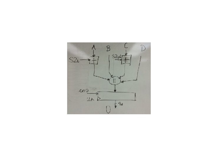
Memories of Round Keys – Circuit S 2 i
Counter 0 m-1 eni en ldi ld reset rst clk m-1 i ==r zi
Interface with the Division into the Datapath and Controller
Pseudocode Split input I into four words, I 3, I 2, I 1, I 0, of the size of w bits each A = I 3; B = I 2; C = I 1; D=I 0 B = B + S[0] D = D + S[1] for i = 1 to r do { T = (B*(2 B + 1)) <<< k U = (D*(2 D + 1)) <<< k A = ((A ⊕ T) <<< U) + S[2 i] C = ((C ⊕ U) <<< T) + S[2 i + 1] (A, B, C, D) = (B, C, D, A) } A = A + S[2 r + 2] C = C + S[2 r + 3] O = (A, B, C, D)
Pseudocode Split input I into four words, I 3, I 2, I 1, I 0, of the size of w bits each A = I 3 B = I 2 + S[0] C = I 1 D = I 0 + S[1] for i = 1 to r do { T = (B*(2 B + 1)) <<< k U = (D*(2 D + 1)) <<< k A’ = ((A ⊕ T) <<< U) + S[2 i] C’ = ((C ⊕ U) <<< T) + S[2 i + 1] (A, B, C, D) = (B, C’, D, A’) } A = A + S[2 r + 2] C = C + S[2 r + 3] O = (A, B, C, D)
Pseudocode Split input I into four words, I 3, I 2, I 1, I 0, of the size of w bits each A = I 3; B = I 2 + S 2 i; C = I 1; D = I 0 + S 2 ip 1 for i = 1 to r do { T = (B*(2 B + 1)) <<< k U = (D*(2 D + 1)) <<< k A’ = ((A ⊕ T) <<< U) + S[2 i] C’ = ((C ⊕ U) <<< T) + S[2 i + 1] (A, B, C, D) = (B, C’, D, A’) } O = (A + S 2 i, B, C + S 2 ip 1, D)
reset S_wait i=0 F S_wait ldi write_I F write_I T T A=I 3; B=I 2+S 2 i C=I 1; D=I 0+S 2 ip 1 i++ S_loop A=B; B=C’ C=D; D=A’ i==r init, enr eni S_loop enr i++ F T i++ S_done O=(A+S 2 i, B, C+S 2 ip 1, D) DONE F zi T eni S_done eno DONE
reset S_wait i=0 F S_wait ldi write_I F write_I T T A=I 3; B=I 2+S 2 i C=I 1; D=I 0+S 2 ip 1 i++ S_loop A=B; B=C’ C=D; D=A’ i++ i==r init, enr eni F T T S_done O=(A+S 2 i, B, C+S 2 ip 1, D) DONE F zi S_done eno DONE
Alternative Coding Styles 74
Traditional Coding Style process(clock, reset) Inputs Next State function Next State clock reset Present State Register Mealy Output function Moore Output function Mealy Outputs Moore Outputs Present State concurrent statements 75
Alternative Coding Style 1 Process(Present State, Inputs) Inputs Next State function Next State clock reset Process(Present State, Inputs) Process(clock, reset) Present State Register Present State Process(Present State) Mealy Output function Moore Output function Mealy Outputs Moore Outputs 76
oe <= 1 RTL Hardware Design by P. Chu Chapter 10 77
78
79
80
81
82
Alternative Coding Style 2 Process(Present State, Inputs) Process(clk, reset) 83
oe <= 1 RTL Hardware Design by P. Chu Chapter 10 84
85
86
87