ECE 545 Lecture 10 FPGA Memories ATHENa Automated


 Block RAM-based (BRAM-based) Memory Inferred")

 RAM blocks DSP units Logic resources")

 32 -bit SR 64 x 1 RAM 64 x 1")


 RAM blocks DSP units Logic resources")

 1 2 0 4 0")


 constraint files testbench database entries (machine-")
 • synthesis, implementation, and timing analysis in batch mode •")
 • automated verification of designs through simulation in batch mode")


 Similar Tools Explore. Ahead (part of Plan. Ahead) Design Space Explorer (DSE)")


 # FUNCTIONAL_VERFICATION_MODE = <on | off> FUNCTIONAL_VERIFICATION_MODE =")
 # MAX_TIME_FUNCTIONAL_VERIFICATION = <$time $unit> # supported unit")


 – K.")


")


")
- Slides: 113
ECE 545 Lecture 10 FPGA Memories ATHENa - Automated Tool for Hardware Evaluatio. N George Mason University
Recommended reading • Spartan-6 FPGA Block RAM Resources: User Guide Google search: UG 383 • Spartan-6 FPGA Configurable Logic Block: User Guide Google search: UG 384 • Xilinx FPGA Embedded Memory Advantages: White Paper Google search: WP 360 2
Recommended reading • XST User Guide for Virtex-6, Spartan-6, and 7 Series Devices Chapter 7, HDL Coding Techniques Sections: • RAM HDL Coding Techniques • ROM HDL Coding Techniques • ISE In-Depth Tutorial, Section: Creating a CORE Generator Tool Module 3
Memory Types 4
Memory Types Memory RAM ROM Memory Single port Dual port Memory With asynchronous read With synchronous read 5
Memory Types specific to Xilinx FPGAs Memory Distributed (MLUT-based) Block RAM-based (BRAM-based) Memory Inferred Instantiated Manually Using CORE Generator 6
FPGA Distributed Memory 7
Location of Distributed RAM Logic resources (CLB slices) RAM blocks DSP units Logic resources (#Logic resources, #Multipliers/DSP units, #RAM_blocks) Graphics based on The Design Warrior’s Guide to FPGAs Devices, Tools, and Flows. ISBN 0750676043 Copyright © 2004 Mentor Graphics Corp. (www. mentor. com) 8
Three Different Types of Slices 50% 25% 9
Spartan-6 Multipurpose LUT (MLUT) 32 -bit SR 64 x 1 RAM 64 x 1 ROM (logic) The Design Warrior’s Guide to FPGAs Devices, Tools, and Flows. ISBN 0750676043 Copyright © 2004 Mentor Graphics Corp. (www. mentor. com) 10
Single-port 64 x 1 -bit RAM 11
Memories Built of Neighboring MLUTs Memories built of 2 MLUTs: • Single-port 128 x 1 -bit RAM: • Dual-port 64 x 1 -bit RAM : RAM 128 x 1 S RAM 64 x 1 D Memories built of 4 MLUTs: • • Single-port 256 x 1 -bit RAM: RAM 256 x 1 S Dual-port 128 x 1 -bit RAM: RAM 128 x 1 D Quad-port 64 x 1 -bit RAM: RAM 64 x 1 Q Simple-dual-port 64 x 3 -bit RAM: RAM 64 x 3 SDP (one address for read, one address for write) 12
Dual-port 64 x 1 RAM • • Dual-port 64 x 1 -bit RAM : Single-port 128 x 1 -bit RAM: 64 x 1 D 128 x 1 S 13
Total Size of Distributed RAM 14
FPGA Block RAM 15
Location of Block RAMs Logic resources (CLB slices) RAM blocks DSP units Logic resources (#Logic resources, #Multipliers/DSP units, #RAM_blocks) Graphics based on The Design Warrior’s Guide to FPGAs Devices, Tools, and Flows. ISBN 0750676043 Copyright © 2004 Mentor Graphics Corp. (www. mentor. com) 16
Spartan-6 Block RAM Amounts 17
Block RAM can have various configurations (port aspect ratios) 1 2 0 4 0 0 4 k x 4 8 k x 2 4, 095 16 k x 1 8, 191 8+1 0 2 k x (8+1) 2047 16+2 0 1023 1024 x (16+2) 16, 383 18
19
20
Block RAM Port Aspect Ratios 21
Block RAM Interface 22
Block RAM Ports 23
Block RAM Waveforms – READ_FIRST mode 24
Block RAM with synchronous read in Read-First Mode CE 25
Block RAM Waveforms – WRITE_FIRST mode 26
Block RAM Waveforms – NO_CHANGE mode 27
Features of Block RAMs in Spartan-6 FPGAs 28
Inference vs. Instantiation 29
30
Using CORE Generator 31
CORE Generator 32
CORE Generator 33
Generic Inferred ROM 34
Distributed ROM with asynchronous read LIBRARY ieee; USE ieee. std_logic_1164. all; USE ieee. std_logic_arith. all; Entity ROM is generic ( w : integer : = 12; -- number of bits per ROM word r : integer : = 3); -- 2^r = number of words in ROM port (addr : in std_logic_vector(r-1 downto 0); dout : out std_logic_vector(w-1 downto 0)); end ROM; 35
Distributed ROM with asynchronous read architecture behavioral of rominfr is type rom_type is array (2**r-1 downto 0) of std_logic_vector (w-1 downto 0); constant ROM_array : rom_type : = ("000011000100", "010011010010", "010011011011", "011011000010", "000011110001", "011111010110", "010011010000", "111110011111"); begin dout <= ROM_array(conv_integer(unsigned(addr))); end behavioral; 36
Distributed ROM with asynchronous read architecture behavioral of rominfr is type rom_type is array (2**r-1 downto 0) of std_logic_vector (w-1 downto 0); constant ROM_array : rom_type : = (X"0 C 4", X"4 D 2", X"4 DB", X"6 C 2", X"0 F 1", X"7 D 6", X"4 D 0", X"F 9 F"); begin dout <= ROM_array(conv_integer(unsigned(addr))); end behavioral; 37
Generic Inferred RAM 38
Distributed versus Block RAM Inference Examples: 1. Distributed single-port RAM with asynchronous read 2. Distributed dual-port RAM with asynchronous read 1. Block RAM with synchronous read (no version with asynchronous read!) More excellent RAM examples from XST Coding Guidelines. 39
Distributed single-port RAM with asynchronous read LIBRARY ieee; USE ieee. std_logic_1164. all; USE ieee. std_logic_arith. all; entity raminfr is generic ( w : integer : = 32; -- number of bits per RAM word r : integer : = 6); -- 2^r = number of words in RAM port (clk : in std_logic; we : in std_logic; a : in std_logic_vector(r-1 downto 0); di : in std_logic_vector(w-1 downto 0); do : out std_logic_vector(w-1 downto 0)); end raminfr; 40
Distributed single-port RAM with asynchronous read architecture behavioral of raminfr is type ram_type is array (2**r-1 downto 0) of std_logic_vector (w-1 downto 0); signal RAM : ram_type; begin process (clk) begin if (clk'event and clk = '1') then if (we = '1') then RAM(conv_integer(unsigned(a))) <= di; end if; end process; do <= RAM(conv_integer(unsigned(a))); end behavioral; 41
Distributed dual-port RAM with asynchronous read library ieee; use ieee. std_logic_1164. all; use ieee. std_logic_unsigned. all; use ieee. std_logic_arith. all; entity raminfr is generic ( w : integer : = 32; -- number of bits per RAM word r : integer : = 6); -- 2^r = number of words in RAM port (clk : in std_logic; we : in std_logic; a : in std_logic_vector(r-1 downto 0); dpra : in std_logic_vector(r-1 downto 0); di : in std_logic_vector(w-1 downto 0); spo : out std_logic_vector(w-1 downto 0); dpo : out std_logic_vector(w-1 downto 0)); end raminfr; 42
Distributed dual-port RAM with asynchronous read architecture syn of raminfr is type ram_type is array (2**r-1 downto 0) of std_logic_vector (w-1 downto 0); signal RAM : ram_type; begin process (clk) begin if (clk'event and clk = '1') then if (we = '1') then RAM(conv_integer(unsigned(a))) <= di; end if; end process; spo <= RAM(conv_integer(unsigned(a))); dpo <= RAM(conv_integer(unsigned(dpra))); end syn; 43
Block RAM with synchronous read in Read-First Mode 44
Block RAM Waveforms – READ_FIRST mode 45
Block RAM with synchronous read LIBRARY ieee; USE ieee. std_logic_1164. all; USE ieee. std_logic_arith. all; entity raminfr is generic ( w : integer : = 32; -- number of bits per RAM word r : integer : = 9); -- 2^r = number of words in RAM port (clk : in std_logic; we : in std_logic; en : in std_logic; addr : in std_logic_vector(r-1 downto 0); di : in std_logic_vector(w-1 downto 0); do : out std_logic_vector(w-1 downto 0)); end raminfr; 46
Block RAM with synchronous read Read-First Mode - cont'd architecture behavioral of raminfr is type ram_type is array (2**r-1 downto 0) of std_logic_vector (w-1 downto 0); signal RAM : ram_type; begin process (clk) begin if (clk'event and clk = '1') then if (en = '1') then do <= RAM(conv_integer(unsigned(addr))); if (we = '1') then RAM(conv_integer(unsigned(addr))) <= di; end if; end process; end behavioral; 47
Block RAM Waveforms – WRITE_FIRST mode 48
Block RAM with synchronous read Write-First Mode - cont'd architecture behavioral of raminfr is type ram_type is array (2**r-1 downto 0) of std_logic_vector (w-1 downto 0); signal RAM : ram_type; begin process (clk) begin if (clk'event and clk = '1') then if (en = '1') then if (we = '1') then RAM(conv_integer(unsigned(addr))) <= di; do <= di; else do <= RAM(conv_integer(unsigned(addr))); end if; end process; end behavioral; 49
Block RAM Waveforms – NO_CHANGE mode 50
Block RAM with synchronous read No-Change Mode - cont'd architecture behavioral of raminfr is type ram_type is array (2**r-1 downto 0) of std_logic_vector (w-1 downto 0); signal RAM : ram_type; begin process (clk) begin if (clk'event and clk = '1') then if (en = '1') then if (we = '1') then RAM(conv_integer(unsigned(addr))) <= di; else do <= RAM(conv_integer(unsigned(addr))); end if; end process; end behavioral; 51
Criteria for Implementing Inferred RAM in BRAMs 52
ATHENa George Mason University
Resources • ATHENa website http: //cryptography. gmu. edu/athena 54
ATHENa – Automated Tool for Hardware Evaluatio. N 55 Supported in part by the National Institute of Standards & Techno
ATHENa Team Venkata “Vinny” MS Cp. E student Ekawat “Ice” Ph. D Cp. E student Marcin John Ph. D ECE student MS Cp. E student Michal Ph. D exchange Ph. D ECE student from Slovakia student Rajesh
ATHENa – Automated Tool for Hardware Evaluatio. N http: //cryptography. gmu. edu/athena Benchmarking open-source tool, written in Perl, aimed at an AUTOMATED generation of OPTIMIZED results for MULTIPLE hardware platforms Currently under development at George Mason University. 57
Why Athena? "The Greek goddess Athena was frequ called upon to settle disputes between the gods or various mortals. Athena G known for her superb logic and intellec Her decisions were usually well-consid highly ethical, and seldom motivated by self-interest. ” from "Athena, Greek Goddess of Wisdom and Craftsmanship" 58
Basic Dataflow of ATHENa User FPGA Synthesis and Implementation 6 5 Database query ATHENa Server 2 Ranking of designs HDL + scripts + configuration files 3 Result Summary + Database Entries 1 Download scripts and configuration files 8 HDL + FPGA Tools 4 Designer Database Entries 0 Interfaces + Testbenches 59
configuration files synthesizable source files result summary (user-friendly) constraint files testbench database entries (machine- friendly) 60
ATHENa Major Features (1) • synthesis, implementation, and timing analysis in batch mode • support for devices and tools of multiple FPGA vendors: • generation of results for multiple families of FPGAs of a given vendor • automated choice of a best-matching device within a given family 61
ATHENa Major Features (2) • automated verification of designs through simulation in batch mode OR • support for multi-core processing • automated extraction and tabulation of results • several optimization strategies aimed at finding – optimum options of tools – best target clock frequency – best starting point of placement 62
Generation of Results Facilitated by ATHENa • batch mode of FPGA tools vs. • ease of extraction and tabulation of results • Text Reports, Excel, CSV (Comma-Separated Values) • optimized choice of tool options • GMU_optimization_1 strategy 63
Relative Improvement of Results from Using ATHENa Virtex 5, 256 -bit Variants of Hash Functions 2. 5 2 1. 5 Area 1 Thr/Area 0. 5 G JH ro e Sh s av tl ite -3 Lu f Ke fa cc a H k am si Ec ho Sk ei Fu n gu e Sh a 2 B C ub MW e. H as h Bl ak Sh e ab a SI l M D 0 Ratios of results obtained using ATHENa suggested options vs. default options of FPGA tools 64
Other (Somewhat) Similar Tools Explore. Ahead (part of Plan. Ahead) Design Space Explorer (DSE) Boldport Flow EDAx 10 Cloud Platform 65
Distinguishing Features of ATHENa • Support for multiple tools from multiple vendors • Optimization strategies aimed at the best possible performance rather than design closure • Extraction and presentation of results • Seamless integration with the ATHENa database of results 66
How To Start Working With ATHENa? One-Time Tasks Download and unzip ATHENa http: //cryptography. gmu. edu/athena/ Read the Tutorial! Install the Required Tools (see Tutorial - Part 1 – Tools Installation) Run ATHENa_setup
How To Start Working With ATHENa? Repetitive Tasks Prepare or modify your source files & source_list. txt Modify design. config. txt + possibly other configuration files Run ATHENa
design. config. txt Your Design # directory containing synthesizable source files for the project SOURCE_DIR = <examples/sha 256_rs> # A file list containing list of files in the order suitable for synthesis and implementation # low level modules first, top level entity last SOURCE_LIST_FILE = source_list. txt # project name # it will be used in the names of result directories PROJECT_NAME = SHA 256 # name of top level entity TOP_LEVEL_ENTITY = sha 256 # name of top level architecture TOP_LEVEL_ARCH = rs_arch # name of clock net CLOCK_NET = clk
design. config. txt Timing Formulas #formula for latency LATENCY = TCLK*65 #formula for throughput THROUGHPUT = 512/(TCLK*65)
design. config. txt Application & Optimization Target # OPTIMIZATION_TARGET = speed | area | balanced OPTIMIZATION_TARGET = speed # OPTIONS = default | user OPTIONS = default # APPLICATION = single_run | exhaustive_search | placement_search | frequency_search | # GMU_Optimization_1 | GMU_Xilinx_optimization_1 APPLICATION = single_run # TRIM_MODE = off | zip | delete TRIM_MODE = zip
design. config. txt FPGA Families # commenting the next line removes all families of Xilinx FPGA_VENDOR = xilinx #commenting the next line removes a given family FPGA_FAMILY = spartan 3 # FPGA_DEVICES = <list of devices> | best_match | all FPGA_DEVICES = best_match SYN_CONSTRAINT_FILE = default IMP_CONSTRAINT_FILE = default REQ_SYN_FREQ = 120 REQ_IMP_FREQ = 100 MAX_SLICE_UTILIZATION = 0. 8 MAX_BRAM_UTILIZATION = 0. 8 MAX_MUL_UTILIZATION = 1 MAX_PIN_UTILIZATION = 0. 9 END FAMILY END VENDOR
design. config. txt FPGA Families # commenting the next line removes all families of Altera FPGA_VENDOR = altera #commenting the next line removes a given family FPGA_FAMILY = Stratix III # FPGA_DEVICES = <list of devices> | best_match | all FPGA_DEVICES = best_match SYN_CONSTRAINT_FILE = default IMP_CONSTRAINT_FILE = default REQ_IMP_FREQ = 120 MAX_LOGIC_UTILIZATION = 0. 8 MAX_MEMORY_UTILIZATION = 0. 8 MAX_DSP_UTILIZATION = 0 MAX_MUL_UTILIZATION = 0 MAX_PIN_UTILIZATION = 0. 8 END FAMILY END VENDOR
Library Files device_lib/xilinx_device_lib. txt device_lib/altera_device_lib. txt • Files created during ATHENa setup • Characterize FPGA families and devices available in the version of Xilinx and Altera tools installed on your computer • Currently supported tool versions: – Xilinx Web. PACK 9. 1, 9. 2, 10. 1, 11. 5, 12. 1, 12. 2, 12. 3, 12. 4, 13. 1, 13. 2, 13. 3, 14. 1, 14. 2, 14. 3 – Xilinx Design Suite 11. 1, 12. 2, 12. 3, 12. 4, 13. 1, 13. 2, 13. 3, 14. 1, 14. 2, 14. 3 – Altera Quartus II Web Edition 8. 1, 8. 2, 9. 0, 9. 1, 10. 0, 10. 1, 11. 0, 11. 1, 12. 0, 12. 1 – Altera Quartus II Subscription Edition 9. 1, 10. 0, 10. 1, 11. 0, 11. 1, 12. 0, 12. 1 • In case a library for a given version not available yet, use a library from the closest available version
Library Files device_lib/xilinx_device_lib. txt VENDOR = Xilinx #Device, Total Slices, Block RAMs, DSP, Dedicated Multipliers, Maximum User I/O Pins ITEM_ORDER = SLICE, BRAM, DSP, MULT, IO FAMILY = spartan 3 xc 3 s 50 pq 208 -5, 768, 4, 0, 4, 124 xc 3 s 200 ft 256 -5, 1920, 12, 173 xc 3 s 400 fg 456 -5, 3584, 16, 0, 16, 264 xc 3 s 1000 fg 676 -5, 7680, 24, 391 xc 3 s 1500 fg 676 -5, 13312, 32, 0, 32, 487 END_FAMILY = virtex 5 xc 5 vlx 30 ff 676 -3, xc 5 vfx 30 tff 665 -3, xc 5 vlx 50 ff 1153 -3, xc 5 vlx 50 tff 1136 -3, END_FAMILY 4800, 32, 5120, 68, 4800, 36, 7200, 48, 7200, 60, 32, 64, 32, 48, 0, 0, 0, 400 360 560 480
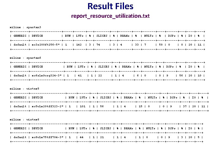
Result Files report_timing. txt REQ SYN REQ IMP LATENCY TP/Area FREQ TCLK - Requested synthesis clk freq. - Requested synthesis clk period - Requested implement. clk freq. - Requested implement. clk period - Latency [ns] - Throughput/Area [(Mbits/s)/CLB slices SYN FREQ – Achieved synthesis clk. freq. SYN TCLK – Achieved synthesis clk. period IMP FREQ – Achieved implement. clk. freq. IMP TCLK – Achieved implement clk. period THROUGHPUT – Throughput [Mbits/s] Latency*Area – Latency*Area [ns*CLB slices] xilinx : spartan 3 +-------------+--------------+----------+--------------+----------+---------+------------+-------+ | GENERIC | DEVICE | RUN | REQ SYN FREQ | REQ SYN TCLK | REQ IMP FREQ | REQ IMP TCLK | LATENCY | THROUGHPUT | TP/Area | Latency*Area | +-------------+--------------+----------+--------------+----------+---------+------------+-------+ | default | xc 3 s 200 ft 256 -5* | 1 | default | 207. 370 | default | 4. 822 | default | 112. 448 | default | 8. 893 | 17. 786 | 449. 792 | 6. 078 | 1316. 164 | +-------------+--------------+----------+--------------+----------+---------+------------+-------+ xilinx : spartan 6 +--------------+--------------+----------+--------------+----------+---------+------------+-------+ | GENERIC | DEVICE | RUN | REQ SYN FREQ | REQ SYN TCLK | REQ IMP FREQ | REQ IMP TCLK | LATENCY | THROUGHPUT | TP/Area | Latency*Area | +--------------+--------------+----------+--------------+----------+---------+------------+-------+ | default | xc 6 slx 9 csg 324 -3* | 1 | default | 75. 751 | default | 13. 201 | default | 78. 119 | default | 12. 801 | 25. 602 | 312. 476 | 14. 203 | 563. 244 | +--------------+--------------+----------+--------------+----------+---------+------------+-------+ xilinx : virtex 5 +--------------+--------------+----------+--------------+----------+---------+------------+-------+ | GENERIC | DEVICE | RUN | REQ SYN FREQ | REQ SYN TCLK | REQ IMP FREQ | REQ IMP TCLK | LATENCY | THROUGHPUT | TP/Area | Latency*Area | +--------------+--------------+----------+--------------+----------+---------+------------+-------+ | default | xc 5 vlx 20 tff 323 -2* | 1 | default | 156. 347 | default | 6. 396 | default | 126. 952 | default | 7. 877 | 15. 754 | 507. 808 | 9. 068 | 882. 224 | +--------------+--------------+----------+--------------+----------+---------+------------+-------+ xilinx : virtex 6 +--------------+--------------+----------+--------------+----------+---------+------------+-------+ | GENERIC | DEVICE | RUN | REQ SYN FREQ | REQ SYN TCLK | REQ IMP FREQ | REQ IMP TCLK | LATENCY | THROUGHPUT | TP/Area | Latency*Area | +--------------+--------------+----------+--------------+----------+---------+------------+-------+ | default | xc 6 vlx 75 tff 784 -3* | 1 | default | 158. 053 | default | 6. 327 | default | 135. 410 | default | 7. 385 | 14. 770 | 541. 638 | 25. 792 | 310. 170 | +--------------+--------------+----------+--------------+----------+---------+------------+-------+
Result Files report_options. txt COST TABLE - parameter determining the starting point of placement Synthesis Options – options of the synthesis tool Map Options – Options of the mapping tool PAR Options – Options of the place & route tool xilinx : spartan 3 +-------------+------------+-------------------------+-------+ | GENERIC | DEVICE | RUN | COST TABLE | Synthesis Options | Map Options | PAR Options | +-------------+------------+-------------------------+-------+ | default | xc 3 s 200 ft 256 -5* | 1 | -opt_level 1 -opt_mode speed | -c 100 -pr b -cm speed | -w -ol std | +-------------+------------+-------------------------+-------+ xilinx : spartan 6 +--------------+--------+---------------+--------+-------+ | GENERIC | DEVICE | RUN | COST TABLE | Synthesis Options | Map Options | PAR Options | +--------------+--------+---------------+--------+-------+ | default | xc 6 slx 9 csg 324 -3* | 1 | -opt_level 1 -opt_mode speed | -c 100 -pr b | -w -ol std | +--------------+--------+---------------+--------+-------+ xilinx : virtex 5 +--------------+------------+-------------------------+-------+ | GENERIC | DEVICE | RUN | COST TABLE | Synthesis Options | Map Options | PAR Options | +--------------+------------+-------------------------+-------+ | default | xc 5 vlx 20 tff 323 -2* | 1 | -opt_level 1 -opt_mode speed | -c 100 -pr b -cm speed | -w -ol std | +--------------+------------+-------------------------+-------+ xilinx : virtex 6 +--------------+------------+---------------+--------+-------+ | GENERIC | DEVICE | RUN | COST TABLE | Synthesis Options | Map Options | PAR Options | +--------------+------------+---------------+--------+-------+ | default | xc 6 vlx 75 tff 784 -3* | 1 | -opt_level 1 -opt_mode speed | -c 100 -pr b | -w -ol std | +--------------+------------+---------------+--------+-------+
Result Files report_execution_time. txt Synthesis Time Implementation Time Elapsed Time - Time of Synthesis - Time of Implementation - Total Time xilinx : spartan 3 +-------------+----------------+--------------+ | GENERIC | DEVICE | RUN | Synthesis Time | Implementation Time | Elapsed Time | +-------------+----------------+--------------+ | default | xc 3 s 200 ft 256 -5* | 1 | 0 d 0 h: 0 m: 12 s | 0 d 0 h: 0 m: 36 s | 0 d 0 h: 0 m: 48 s | +-------------+----------------+--------------+ xilinx : spartan 6 +--------------+----------------+--------------+ | GENERIC | DEVICE | RUN | Synthesis Time | Implementation Time | Elapsed Time | +--------------+----------------+--------------+ | default | xc 6 slx 9 csg 324 -3* | 1 | 0 d 0 h: 0 m: 21 s | 0 d 0 h: 1 m: 13 s | 0 d 0 h: 1 m: 34 s | +--------------+----------------+--------------+ xilinx : virtex 5 +--------------+----------------+--------------+ | GENERIC | DEVICE | RUN | Synthesis Time | Implementation Time | Elapsed Time | +--------------+----------------+--------------+ | default | xc 5 vlx 20 tff 323 -2* | 1 | 0 d 0 h: 0 m: 39 s | 0 d 0 h: 1 m: 50 s | 0 d 0 h: 2 m: 29 s | +--------------+----------------+--------------+ xilinx : virtex 6 +--------------+----------------+--------------+ | GENERIC | DEVICE | RUN | Synthesis Time | Implementation Time | Elapsed Time | +--------------+----------------+--------------+ | default | xc 6 vlx 75 tff 784 -3* | 1 | 0 d 0 h: 0 m: 22 s | 0 d 0 h: 3 m: 44 s | +--------------+----------------+--------------+
design. config. txt Functional Simulation (1) # FUNCTIONAL_VERFICATION_MODE = <on | off> FUNCTIONAL_VERIFICATION_MODE = <off> # directory containing source files of the testbench VERIFICATION_DIR = <examples/sha 256_rs/tb> # A file containing a list of testbench files in the order suitable for compilation; # low level modules first, top level entity last. # Test vector files should be located in the same directory and listed # in the same file, unless fixed path is used. Please refer to tutorial for more detail. VERIFICATION_LIST_FILE = <tb_srcs. txt> # name of testbench's top level entity TB_TOP_LEVEL_ENTITY = <sha_tb> # name of testbench's top level architecture TB_TOP_LEVEL_ARCH = <behavior>
design. config. txt Functional Simulation (2) # MAX_TIME_FUNCTIONAL_VERIFICATION = <$time $unit> # supported unit are : ps, ns, us, and ms # if blank, simulation will run until it finishes = # = no changes in signals, i. e. , clock is stopped and no more inputs coming in. MAX_TIME_FUNCTIONAL_VERIFICATION = <> # Perform only verification (synthesis and implementation parameters are ignored) # VERIFICATION_ONLY = <ON | OFF> VERIFICATION_ONLY = <off>
ATHENa – Database of Results 82
ATHENa Database http: //cryptography. gmu. edu/athenadb 83
ATHENa Database – Result View • Algorithm parameters • Design parameters § Optimization target § Architecture type § Datapath width § I/O bus widths § Availability of source code § Platform § Vendor, Family, Device § Timing § Maximum clock frequency § Maximum throughput § Resource utilization § Logic blocks (Slices/LEs/ALUTs) § Multipliers/DSP units § Tools § Names & versions § Detailed options § Credits § Designers & contact information 84
ATHENa Database – Compare Feature Matching fields in grey Non-matching fields in red and blue 85
Possible Future Customizations The same basic database can be customized and adapted for other domains, such as • Digital Signal Processing • Bioinformatics • Communications • Scientific Computing, etc. 86
ATHENa - Website 87
ATHENa Website http: //cryptography. gmu. edu/athena/ • Download of ATHENa Tool • Links to related tools SHA-3 Competition in FPGAs & ASICs • Specifications of candidates • Interface proposals • RTL source codes • Testbenches • ATHENa database of results • Related papers & presentations 88
GMU Source Codes and Block Diagrams • GMU Source Codes for all Round 3 SHA-3 Candidates & SHA-2 made available at the ATHENa website at: http: //cryprography. gmu. edu/athena • Included in this release: • Basic architectures • Folded architectures • Unrolled architectures • Each code supports two variants: with 256 -bit and 512 -bit output. • Each source code accompanied by comprehensive hierarchical block diagrams 89
ATHENa Result Replication Files • Scripts and configuration files sufficient to easily reproduce all results (without repeating optimizations) • Automatically created by ATHENa for all results generated using ATHENa • Stored in the ATHENa Database In the same spirit of Reproducible Research as: • J. Claerbout (Stanford University) “Electronic documents give reproducible research a new meaning, ” in Proc. 62 nd Ann. Int. Meeting of the Soc. of Exploration Geophysics, 1992, http: //sepwww. stanford. edu/doku. php? id=sep: research: reproducible: seg 92. . . • Patrick Vandewalle 1, Jelena Kovacevic 2, and Martin Vetterli 1 (1 EPFL, 2 CMU) Reproducible research in signal processing - what, why, and how. IEEE Signal Processing Magazine, May 2009. http: //rr. epfl. ch/17/ 90
Benchmarking Goals Facilitated by ATHENa Comparing multiple: 1. cryptographic algorithms 2. hardware architectures or implementations of the same cryptographic algorithm 3. hardware platforms from the point of view of their suitability for the implementation of a given algorithm, (e. g. , choice of an FPGA device or FPGA board) 4. tools and languages in terms of quality of results they generate (e. g. Verilog vs. VHDL, Synplicity Synplify Premier vs. Xilinx XST, ISE v. 13. 1 vs. ISE v. 12. 3) 91
Modern FPGA Families George Mason University
Major FPGA Vendors SRAM-based FPGAs ~ 51% of the market • Xilinx, Inc. ~ 85% • Altera Corp. ~ 34% of the market • Lattice Semiconductor • Atmel • Achronix • Tabula Flash & antifuse FPGAs • Actel Corp. (Microsemi So. C Products Group) • Quick Logic Corp. ECE 448 – FPGA and ASIC Design with VHDL 93
Xilinx FPGA Devices Technology Low-cost High-performance 220 nm Spartan II Virtex 120/150 nm 90 nm Virtex II, II Pro Spartan 3 65 nm 45 nm Virtex 5 Spartan 6 40 nm 28 nm Virtex 4 Virtex 6 Artix 7 Virtex 7
Altera FPGA Devices Technology Low-cost Mid-range Highperformance 130 nm Cyclone Stratix 90 nm Cyclone II Stratix II 65 nm Cyclone III Arria I Stratix III 40 nm Cyclone IV Arria II Stratix IV 28 nm Cyclone V Arria V Stratix V
Resources Xcell Journal available for FREE on line @ http: //www. xilinx. com/about/xcell-publications/xcell-journal. html Electronic Engineering Journal available for FREE by e-mail after subscribing @ http: //www. eejournal. com/subscribe or on the web @ http: //www. eejournal. com/design/fpga 96
Follow-up Courses George Mason University
ECE Department Programs MS in Electrical Engineering MS EE MS in Computer Engineering MS Cp. E BIOENGINEERING DIGITAL SYSTEMS DESIGN COMMUNICATIONS & NETWORKING MICROPROCESSORS & EMBEDDED SYSTEMS SIGNAL PROCESSING DIGITAL SIGNAL PROCESSING CONTROL & ROBOTICS COMPUTER NETWORKS MICROELECTRONICS/ NANOELECTRONICS NETWORK & SYSTEM SECURITY SYSTEM DESIGN Specializations
DIGITAL SYSTEMS DESIGN 1. ECE 545 Digital System Design with VHDL (Fall) – K. Gaj, project, FPGA design with VHDL, Aldec/Synplicity/Xilinx/Altera 2. ECE 645 Computer Arithmetic (Spring) – K. Gaj, project, FPGA design with VHDL or Verilog, Aldec/Synplicity/Xilinx/Altera 3. ECE 586 Digital Integrated Circuits (Spring) – D. Ioannou 4. ECE 681 VLSI Design for ASICs (Fall) – H. Homayoun, project/lab, front-end and back-end ASIC design with Synopsys tools 1. 5. ECE 682 VLSI Test Concepts (Spring) – T. Storey, homework 2. 6. ECE 699 Digital Signal Processing Hardware Architectures (Spring) – A. Cohen, project, FPGA design with VHDL or Verilog
DIGITAL SIGNAL PROCESSING Concentration advisors: Aaron Cohen, Kris Gaj, Ken Hintz, Jill Nelson, Kathleen Wage 1. ECE 535 Digital Signal Processing – L. Griffiths, J. Nelson, Matlab 2. ECE 545 Digital System Design with VHDL – K. Gaj, project, FPGA design with VHDL 3. ECE 645 Computer Arithmetic – K. Gaj, project, FPGA design with VHDL 4. ECE 699 Digital Signals Processing Hardware Architectures – A. Cohen, project, FPGA design with VHDL and Matlab/Simulink 5 a. ECE 537 Introduction to Digital Image Processing – K. Hintz 5 b. ECE 738 Advanced Digital Signal Processing – K. Wage
Possible New Graduate Computer Engineering Courses • 5 xx Digital System Design with Verilog • 6 xx Reconfigurable Computing (looking for instructors)
NETWORK AND SYSTEM SECURITY 1. ECE 542 Computer Network Architectures and Protocols (Fall, Spring) – S. -C. Chang, et al. 2. ECE 646 Cryptography and Computer Network Security (Fall) – K. Gaj, J-P. Kaps – lab, project: software/hardware/analytical 3. ECE 746 Advanced Applied Cryptography (every 2 nd Spring, 2015) – K. Gaj, J-P. Kaps – lab, project: software/hardware/analytical 4. ECE 699 Cryptographic Engineering (every 2 nd Spring, 2014) – J-P. Kaps – lectures + student/invited guests seminars 5. ISA 656 Network Security (Fall, Spring) – A. Stavrou
ECE 645 Computer Arithmetic Instructor: Dr. Kris Gaj
Advanced digital circuit design course covering Efficient architectures for • addition and subtraction • multiplication • division and modular reduction • exponentiation Integers unsigned and signed Real numbers Elements of the Galois field GF(2 n) • fixed point • single and double precision floating point • polynomial base
Course Objectives At the end of this course you should be able to: • Understand mathematical and gate-level algorithms for computer addition, subtraction, multiplication, division, and exponentiation • Understand tradeoffs involved with different arithmetic architectures between performance, area, latency, scalability, etc. • Synthesize and implement computer arithmetic blocks on FPGAs • Be comfortable with different number systems, and have familiarity with floating-point and Galois field arithmetic for future study • Understand sources of error in computer arithmetic and basics of error analysis This knowledge will come about through homework, project and practice exams.
Lecture topics INTRODUCTION 1. Applications of computer arithmetic algorithms. Initial Discussion of Project Topics.
ADDITION AND SUBTRACTION 1. Basic addition, subtraction, and counting 2. Addition in Xilinx and Altera FPGAs 3. Carry-lookahead, carry-select, and hybrid adders 4. Adders based on Parallel Prefix Networks 5. Pipelined Adders 6. Modular addition and subtraction
MULTIOPERAND ADDITION 1. Carry-save adders 2. Wallace and Dadda Trees 3. Adding multiple unsigned and signed numbers
NUMBER REPRESENTATIONS • Unsigned Integers • Signed Integers • Fixed-point real numbers • Floating-point real numbers • Elements of the Galois Field GF(2 n)
LONG INTEGER ARITHMETIC 1. Modular Exponentiation 2. Montgomery Multipliers and Exponentiation Units
MULTIPLICATION 1. Tree and array multipliers 2. Sequential multipliers 3. Multiplication of signed numbers and squaring 4. Multiplication in Xilinx and Altera FPGAs - using distributed logic - using embedded multipliers - using DSP blocks 5. Multiple clock systems
DIVISION 1. Basic restoring and non-restoring sequential dividers 2. SRT and high-radix dividers 3. Array dividers 4. Division by Convergence
FLOATING POINT AND GALOIS FIELD ARITHMETIC 1. Floating-point units 2. Galois Field GF(2 n) units