Combinational Logic Design Using VHDL Decoders Introduction A
")
Combinational Logic Design (Using VHDL)

Decoders

Introduction • A decoder is a multiple-input, multiple-output logic circuit that converts coded inputs into coded outputs, where the input and output codes are different. • The input code generally has fewer bits than the output code, and there is a one-to -one mapping from input code words into output code words. In a one-to-one mapping, each input code word produces a different output code word. • The enable inputs, if present, must be asserted for the decoder to perform its normal mapping function. • The most commonly used input code is an n-bit binary code, where an n-bit word represents one of 2 n different coded values, normally the integers from 0 through 2 n-1. • Sometimes an n-bit binary code is truncated to represent fewer than 2 n values. For example, in the BCD code, the 4 -bit combinations 0000 through 1001 represent the decimal digits 0– 9, and combinations 1010 through 1111 are not used. • The most commonly used output code is a 1 -out-of-m code, which contains m bits, where one bit is asserted at any time. In a 1 -out-of-4 code with active-high outputs, the code words are 0001, 0010, 0100, and 1000. • With active-low outputs, the code words are 1110, 1101, 1011, and 0111.

Decoder Circuit Structure and its truth table • The most common decoder circuit is an n-to-2 n decoder or binary decoder. Such a decoder has an n-bit binary input code and a 1 -out-of-2 n output code. A binary decoder is used when you need to activate exactly one of 2 n outputs based on an n-bit input value.

VHDL Program
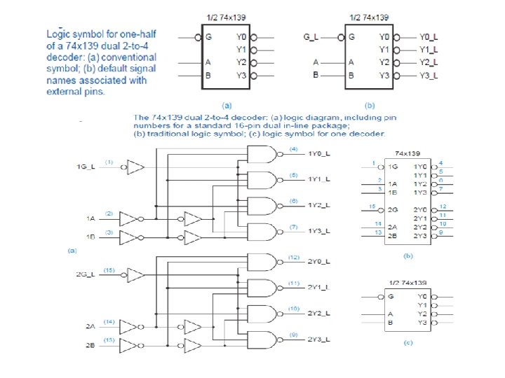

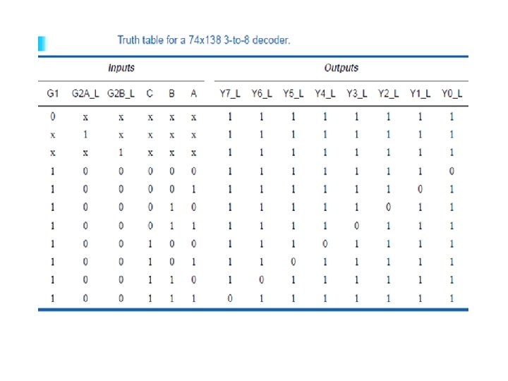
74 x 138 Decoder – an MSI 3 -to-8 decoder
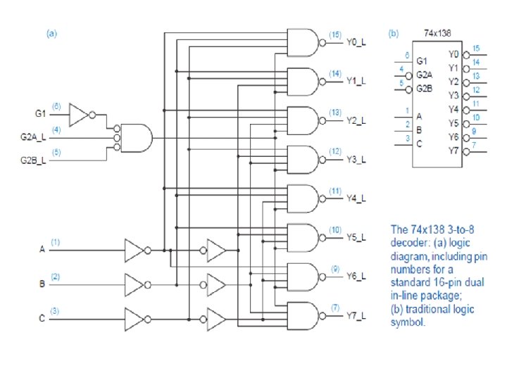

VHDL Program for IC 74 x 138 Process(G 1, G 2 A_L, G 2 B_L, A) Begin case A is when "000" => Y_L_i <= “ 01111111"; when "001" => Y_L_i <= “ 10111111"; when "010" => Y_L_i <= “ 11011111"; when "011" => Y_L_i <= “ 11101111"; when "100" => Y_L_i <= “ 11110111"; when "101" => Y_L_i <= “ 11111011"; when "110" => Y_L_i <= “ 11111101"; when "111" => Y_L_i <= “ 11111110"; when others => Y_L_i <= “ 1111"; end case; if (G 1 and G 2 and G 3)='1' then Y_L <= Y_L_i; else Y <= “ 1111"; end if; end process;
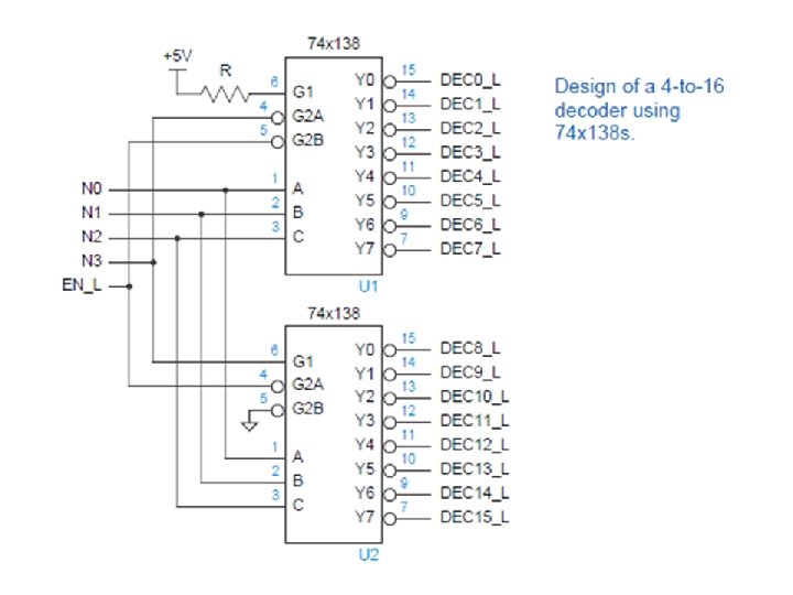

Design of 5 -to-32 decoder using 74 x 138 s and a 74 x 139

Encoders

Introduction • If the device’s output code has fewer bits than the input code, the device is usually called an encoder. • Probably the simplest encoder to build is a 2 nto-n or binary encoder.

Priority Encoder • The 1 -out-of-2 n coded outputs of an n-bit binary decoder are generally used to control a set of 2 n devices, where at most one device is supposed to be active at any time. Conversely, consider a system with 2 n inputs, each of which indicates a request for service. • when multiple requests are asserted, assign priority to the input lines, the encoding device produces the number of the highest-priority requestor. Such a device is called a priority encoder. • Input I 7 has the highest priority. Outputs A 2–A 0 contain the number of the highest-priority asserted input, if any. The IDLE output is asserted if no inputs are asserted. First define eight intermediate variables H 0–H 7, such that Hi is 1 if and only if Ii is the highest priority 1 input: • H 7=I 7 H 6=I 6∙I 7’ H 5=I 5∙I 6’∙I 7’ H 4=I 4∙ I 5’∙I 6’∙I 7’ H 3=I 3∙I 4’∙ I 5’∙I 6’∙I 7’ H 2=I 2∙I 3’∙I 4’∙ I 5’∙I 6’∙I 7’ H 1=I 1∙I 2’∙I 3’∙I 4’∙ I 5’∙I 6’∙I 7’ H 0=I 0∙I 1’∙I 2’∙I 3’∙I 4’∙ I 5’∙I 6’∙I 7’
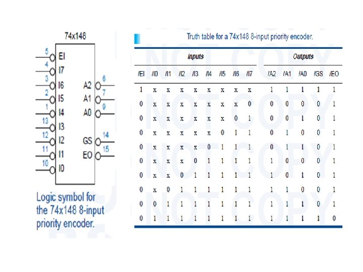

Logic Diagram for the 74 x 148 8 -input priority encoder, including pin numbers for a standard 16 -pin dual-in -line package

MULTIPLEXERS
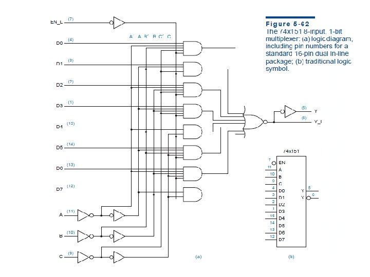

VHDL Program for a 8 -input, 1 -bit multiplexer Library ieee; Use ieee. std_logic_1164. all; Entity mux 8 in 1 bit is Port( EN_L: in std_logic; S: in std_logic_vector(2 downto 0); D: in std_logic_vector(7 downto 0); Y: out std_logic); End mux 8 in 1 bit; Architecture dataflow of mux 8 in 4 bit is Signal y 1: std_logic; Begin with S select Y 1<= D(7) when “ 111”, D(6) when “ 110”, D(5) when “ 101”, D(4) when “ 100”, D(3) when “ 011”, D(2) when “ 010”, D(1) when “ 001”, D(0) when “ 000”, ‘ 0’ when others; y<=y 1 when EN_L=‘ 0’ else ‘ 0’; End dataflow; Library ieee; Use ieee. std_logic_1164. all; Entity mux 8 in 1 bit is Port( EN_L: in std_logic; S: in std_logic_vector(2 downto 0); D: in std_logic_vector(7 downto 0); Y: out std_logic); End mux 8 in 1 bit; Architecture behav of mux 8 in 4 bit is Begin Process(EN_L, S, D) Begin Case S is When “ 111” => Y 1<= D(7) ; When “ 110” => Y 1<= D(6) ; When “ 101” => Y 1<= D(5) ; When “ 100” => Y 1<= D(4) ; When “ 011” => Y 1<= D(3) ; When “ 010” => Y 1<= D(2) ; When “ 001” => Y 1<= D(1) ; When “ 000” => Y 1<= D(0) ; when others => Y 1<=‘ 0’; End case; If(EN_L=‘ 0’) then Y<=Y 1; Else Y<=‘ 0’; End behav;

VHDL behavioral description of a 6 -function barrel shifter: use IEEE. std_logic_1164. all; use IEEE. std_logic_arith. all; entity barrel 16 is port ( DIN: in STD_LOGIC_VECTOR (15 downto 0); -Data inputs S: in UNSIGNED (3 downto 0); -- Shift amount, 015 C: in STD_LOGIC_VECTOR (2 downto 0); -- Mode control DOUT: out STD_LOGIC_VECTOR (15 downto 0) -Data bus output); constant Lrotate: STD_LOGIC_VECTOR : = "000"; - Define the coding of constant Rrotate: STD_LOGIC_VECTOR : = "001"; -- different shift modes constant Llogical: STD_LOGIC_VECTOR : = "010"; constant Rlogical: STD_LOGIC_VECTOR : = "011"; constant Larith: STD_LOGIC_VECTOR : = "100"; constant Rarith: STD_LOGIC_VECTOR : = "101"; end barrel 16; architecture barrel 16_behavioral of barrel 16 is subtype DATAWORD is STD_LOGIC_VECTOR(15 downto 0); function Vrol (D: DATAWORD; S: UNSIGNED) return DATAWORD is variable N: INTEGER; variable TMPD: DATAWORD; begin N : = CONV_INTEGER(S); TMPD : = D; for i in 1 to N loop TMPD : = TMPD(14 downto 0) & TMPD(15); end loop; return TMPD; end Vrol; . . . begin process(DIN, S, C) begin case C is when Lrotate => DOUT <= Vrol(DIN, S); when Rrotate => DOUT <= Vror(DIN, S); when Illogical => DOUT <= Vsll(DIN, S); when Rlogical => DOUT <= Vsrl(DIN, S); when Larith => DOUT <= Vsla(DIN, S); when Rarith => DOUT <= Vsra(DIN, S); when others => DOUT <= DIN; end case; end process; end barrel 16_behavioral;

VHDL program for a 16 -bit barrel shifter for left circular shifts only: library IEEE; use IEEE. std_logic_1164. all; entity rol 16 is port ( DIN: in STD_LOGIC_VECTOR(15 downto 0); -- Data inputs S: in STD_LOGIC_VECTOR (3 downto 0); -- Shift amount, 0 -15 DOUT: out STD_LOGIC_VECTOR(15 downto 0) -- Data bus output); end rol 16; architecture rol 16_arch of rol 16 is begin process(DIN, S) variable X, Y, Z: STD_LOGIC_VECTOR(15 downto 0); begin if S(0)='1' then X : = DIN(14 downto 0) & DIN(15); else X : = DIN; end if; if S(1)='1' then Y : = X(13 downto 0) & X(15 downto 14); else Y : = X; end if; if S(2)='1' then Z : = Y(11 downto 0) & Y(15 downto 12); else Z : = Y; end if; if S(3)='1' then DOUT <= Z(7 downto 0) & Z(15 downto 8); else DOUT <= Z; end if; end process; end rol 16_arch;
")
Sequential Logic Design (Using VHDL)

Difference between combinational and sequential logic circuits A combinational logic circuit is one whose outputs depend only on its current inputs. A sequential logic circuit is one whose outputs depend not only on its current inputs, but also on the past sequence of inputs, possibly arbitrarily far back in time. Eg: The rotary channel selector knob on an old-fashioned TV is like a combinational circuit—its “output” selects a channel based only on its current “input”—the position of the knob. Eg: The circuit controlled by the channel-up and channeldown pushbuttons on a TV or VCR is a sequential circuit—the channel selection depends on the past sequence of up/down pushes, at least since when you started viewing 10 hours before, and perhaps as far back as when you first plugged the device into the wall. It is convenient to describe the behavior of a sequential circuit by means of a table that lists outputs as a function of the input sequence. It is inconvenient, and often impossible, to describe the behavior of a sequential circuit by means of a table that lists outputs as a function of the input sequence that has been received up until the current time.

Clock signals

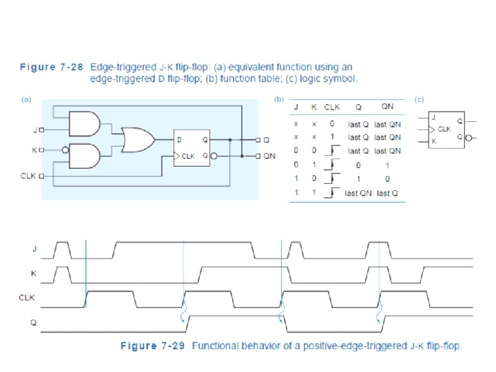
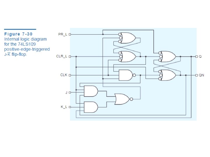
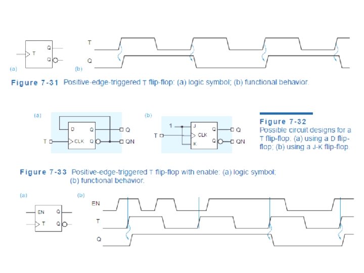
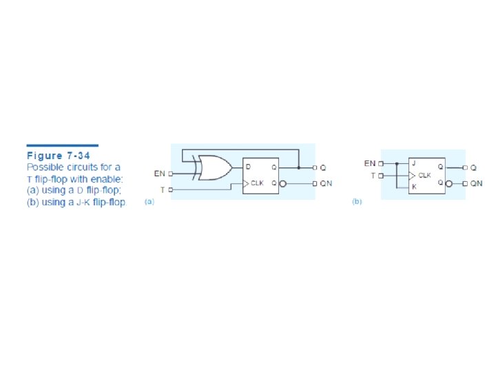
Latches and Flip-Flops Latches Flip-Flops Latch is a device which is used as switch Flip-flop is a storing element They are sensitive to the duration of pulse and can transfer data until they are switched on. They hold the last logic at the output if we put it off(bring the strobe pin to low). They are sensitive to signal change(low to high or high to low) and not the level. Hence they transfer data only at that instant and it cannot be changed until next signal change. They are used as temporary buffers. They are used as registers Latch works without clock signal, but works with a control signal and it is level triggered device. Flip flop is a 1 bit storage element and works with a clock signal. its a edge triggered device. Latches are avoided. Flip flops are preferred. Latch is an asynchronous device and does not need to be synchronized with a clock input. It may have an enable (low or high) and the latch will store the input to the latch when the enable is in its active state. Flip-flop is synchronous and will change states in synch with a clock on either the low-high edge or high-low edge of the clock, depending if the flip-flop is positive or negative edge triggered. By level sensitive we mean that output will respond to change in input as long as the control signal is high. Control signal can be a clock in case of flip flop or any other asynchronous signal in case of latch. By edge sensitive we mean that output will only respond to input at the point when the control signal goes to high from low. Now when the control signal is high the output will not change with change in input. It will again change at the next rising edge of the clock.

Basic SR latch

SR latch with enable

Contd. ,

D latch

Positive edge triggered D Flip-Flop

Negative edge triggered D Flip-Flop

Positive edge triggered D flip-Flop – IC 74 LS 74

Shift Registers

MSI Shift Registers
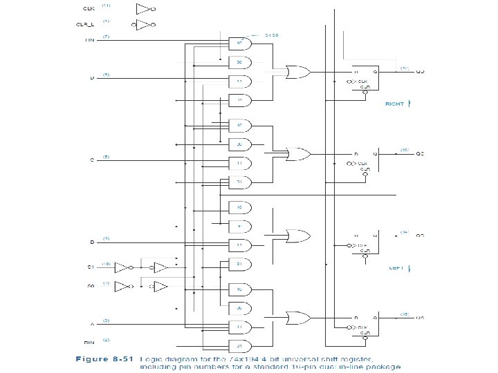

case s is when “ 00” => qn 1<=q ; When “ 01” => qn 1<= RIN & q(3 downto 1); When “ 10” => qn 1<= q(2 downto 0) & LIN; When “ 11” => qn 1<= d; end case;
- Slides: 43