UNITIII COMBINATIONAL LOGIC DESIGN Decoders Introduction A decoder

UNIT-III COMBINATIONAL LOGIC DESIGN

Decoders

Introduction • A decoder is a multiple-input, multiple-output logic circuit that converts coded inputs into coded outputs, where the input and output codes are different. • The input code generally has fewer bits than the output code, and there is a one-to -one mapping from input code words into output code words. In a one-to-one mapping, each input code word produces a different output code word. • The enable inputs, if present, must be asserted for the decoder to perform its normal mapping function. • The most commonly used input code is an n-bit binary code, where an n-bit word represents one of 2 n different coded values, normally the integers from 0 through 2 n-1. • Sometimes an n-bit binary code is truncated to represent fewer than 2 n values. For example, in the BCD code, the 4 -bit combinations 0000 through 1001 represent the decimal digits 0– 9, and combinations 1010 through 1111 are not used. • The most commonly used output code is a 1 -out-of-m code, which contains m bits, where one bit is asserted at any time. In a 1 -out-of-4 code with active-high outputs, the code words are 0001, 0010, 0100, and 1000. • With active-low outputs, the code words are 1110, 1101, 1011, and 0111.

Decoder Circuit Structure and its truth table • The most common decoder circuit is an n-to-2 n decoder or binary decoder. Such a decoder has an n-bit binary input code and a 1 -out-of-2 n output code. A binary decoder is used when you need to activate exactly one of 2 n outputs based on an n-bit input value.

VHDL Program
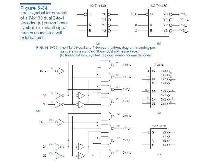

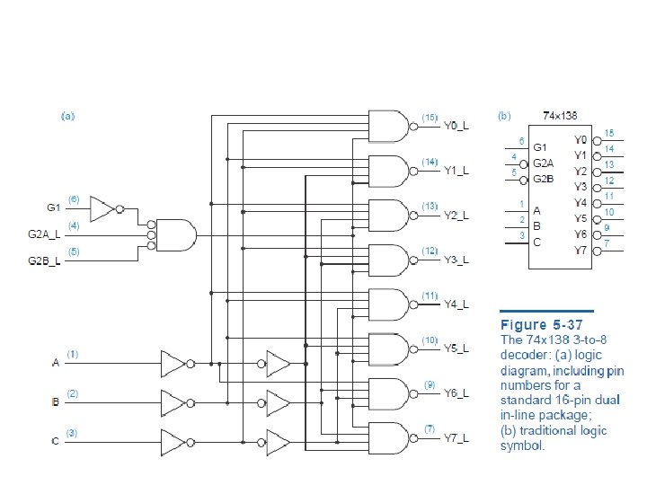
74 x 138 Decoder – an MSI 3 -to-8 decoder
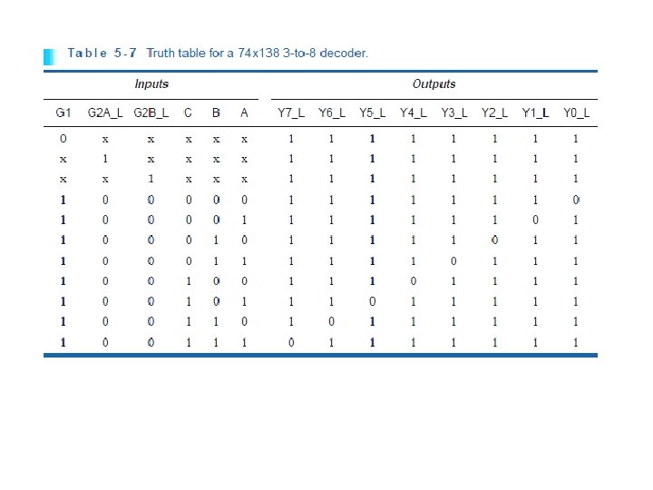

VHDL Program for IC 74 x 138 Process(G 1, G 2 A_L, G 2 B_L, A) Begin case A is when "000" => Y_L_i <= “ 01111111"; when "001" => Y_L_i <= “ 10111111"; when "010" => Y_L_i <= “ 11011111"; when "011" => Y_L_i <= “ 11101111"; when "100" => Y_L_i <= “ 11110111"; when "101" => Y_L_i <= “ 11111011"; when "110" => Y_L_i <= “ 11111101"; when "111" => Y_L_i <= “ 11111110"; when others => Y_L_i <= “ 1111"; end case; if (G 1 and G 2 and G 3)='1' then Y_L <= Y_L_i; else Y <= “ 1111"; end if; end process;
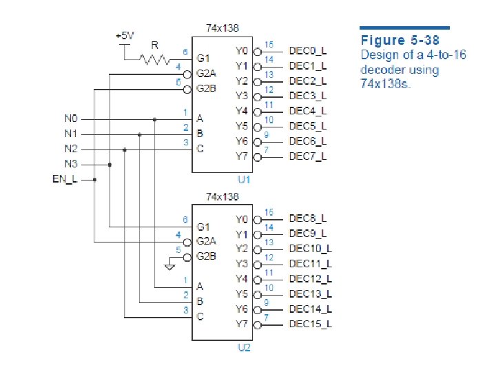

Design of 5 -to-32 decoder using 74 x 138 s and a 74 x 139

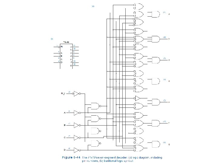
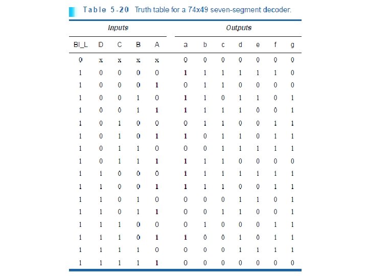
Seven Segment Decoders • A seven-segment decoder has 4 -bit BCD as its input code and the “seven segment code”. • The “blanking input” BI_L, each output of the 74 x 49 is a minimal product-of-sums realization for the corresponding segment, assuming “don’t-cares” for the non-decimal input combinations.

Encoders

Introduction • If the device’s output code has fewer bits than the input code, the device is usually called an encoder. • Probably the simplest encoder to build is a 2 nto-n or binary encoder.

Priority Encoder • The 1 -out-of-2 n coded outputs of an n-bit binary decoder are generally used to control a set of 2 n devices, where at most one device is supposed to be active at any time. Conversely, consider a system with 2 n inputs, each of which indicates a request for service. • when multiple requests are asserted, assign priority to the input lines, the encoding device produces the number of the highest-priority requestor. Such a device is called a priority encoder. • Input I 7 has the highest priority. Outputs A 2–A 0 contain the number of the highest-priority asserted input, if any. The IDLE output is asserted if no inputs are asserted. First define eight intermediate variables H 0–H 7, such that Hi is 1 if and only if Ii is the highest priority 1 input: • H 7=I 7 H 6=I 6∙I 7’ H 5=I 5∙I 6’∙I 7’ H 4=I 4∙ I 5’∙I 6’∙I 7’ H 3=I 3∙I 4’∙ I 5’∙I 6’∙I 7’ H 2=I 2∙I 3’∙I 4’∙ I 5’∙I 6’∙I 7’ H 1=I 1∙I 2’∙I 3’∙I 4’∙ I 5’∙I 6’∙I 7’ H 0=I 0∙I 1’∙I 2’∙I 3’∙I 4’∙ I 5’∙I 6’∙I 7’
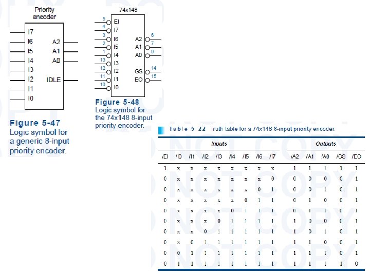

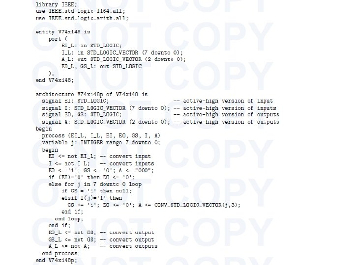
Logic Diagram for the 74 x 148 8 -input priority encoder, including pin numbers for a standard 16 -pin dual-in -line package

Four 74 x 148 s cascaded to handle 32 requests

Three-State Devices

Three-State Buffers • The most basic three-state device is a three-state buffer, or a three-state driver. • When the enable input is asserted, the device behaves like an ordinary buffer or inverter. When the enable input is negated, the device output “floats”; that is, it goes to a high-impedance (Hi-Z), disconnected state and functionally behaves as if it weren’t even there.

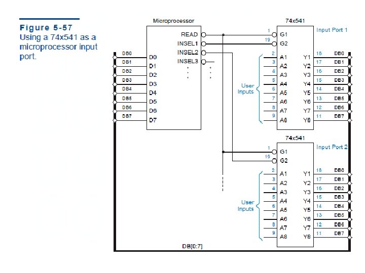
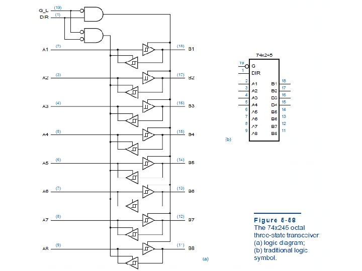
Standard SSI and MSI Three-State Buffers • Like logic gates, several independent three-state buffers may be packaged in a single SSI IC. The pinouts of 74 x 125 and 74 x 126, each of which contains four independent noninverting three-state buffers in a 14 -pin package. • The three-state enable inputs in the ’ 125 are active low, and in the ’ 126 they are active high. • Most party-line applications use a bus with more than one bit of data. • For example, in an 8 -bit microprocessor system, the data bus is eight bits wide, and peripheral devices normally place data on the bus eight bits at a time. • Thus, a peripheral device enables eight three-state drivers to drive the bus, all at the same time. Independent enable inputs, as in the ’ 125 and ’ 126, are not necessary. • Thus, to reduce the package size in wide-bus applications, most commonly used MSI parts contain multiple three-state buffers with common enable inputs.

* 74 x 540 is identical to 74 x 541 except that it has inverting buffers

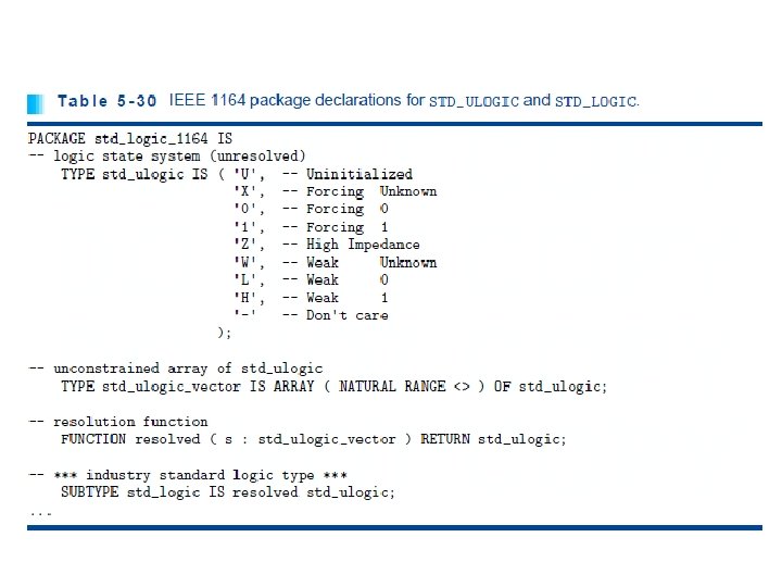
VHDL Program Library ieee; Use ieee. std_logic_1164. all; Entity IC 74541 is Port(a: in std_logic_vector(7 downto 0); G 1_L, G 2_L: in std_logic; y: out std_logic_vector(7 downto 0)); End IC 74541; Architecture behav of IC 74541 is Begin Process(a, G 1_L, G 2_L) Begin If(G 1_L=‘ 0’ and G 2_L=‘ 0’ ) then y<=a; else Y<=“ZZZZ”; End if; End process; End behav;

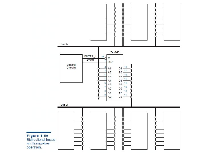
Library ieee; Use ieee. std_logic_1164. all; VHDL Program Entity IC 74245 is Port(G_L, DIR: in std_logic; A, B: inout std_logic_vector(7 downto 0); y: out std_logic_vector(7 downto 0)); End IC 74245; Architecture behav of IC 74245 is Begin Process(G_L, DIR, A, B) Begin If(G_L=‘ 0’) then If(DIR=‘ 0’ ) then A<=B; Elsif (DIR=‘ 1’) then B<=A; End if; Else if (G_L=‘ 1’) then If(DIR=‘ 0’ ) then y<=A; Elsif (DIR=‘ 1’) then y<=B; End if; End process; End behav; * neither bus is ever driven simultaneously by two devices. However, independent transfers where both buses are driven at the same time may occur when the transceiver is disabled, as indicated in the last row of the table.

VHDL Program with four 8 -bit three state drivers library IEEE; use IEEE. std_logic_1164. all; entity V 3 statex is port ( G_L: in STD_LOGIC; -- Global output enable SEL: in STD_LOGIC_VECTOR (1 downto 0); -- Input select 0, 1, 2, 3 ==> A, B, C, D: in STD_LOGIC_VECTOR (1 to 8); -- Input buses X: out STD_ULOGIC_VECTOR (1 to 8) -- Output bus (three-state) ); end V 3 statex; architecture V 3 states of V 3 statex is constant ZZZZ: STD_ULOGIC_VECTOR : = ('Z', 'Z', 'Z'); begin process (G_L, SEL, A) begin if G_L='0' and SEL = "00" then X <= To_Std. ULogic. Vector(A); else X <= ZZZZ; end if; end process; process (G_L, SEL, B) begin if G_L='0' and SEL = "01" then X <= To_Std. ULogic. Vector(B); else X <= ZZZZ; end if; end process; process (G_L, SEL, C) begin if G_L='0' and SEL = "10" then X <= To_Std. ULogic. Vector(C); else X <= ZZZZ; end if; end process; process (G_L, SEL, D) begin if G_L='0' and SEL = "11" then X <= To_Std. ULogic. Vector(D); else X <= ZZZZ; end if; end process; end V 3 states;

MULTIPLEXERS

Multiplexers • A multiplexer is a digital switch—it connects data from one of n sources to its output. • There are n sources of data, each of which is b bits wide, and there are b output bits. In typical commercially available multiplexers, n = 1, 2, 4, 8, or 16, and b = 1, 2, or 4. There are s inputs that select among the n sources, so s = [log 2 n]. An enable input EN allows the multiplexer to “do its thing”; when EN = 0, all of the outputs are 0. • Applications: in computers between the processor’s registers and its arithmetic logic unit.

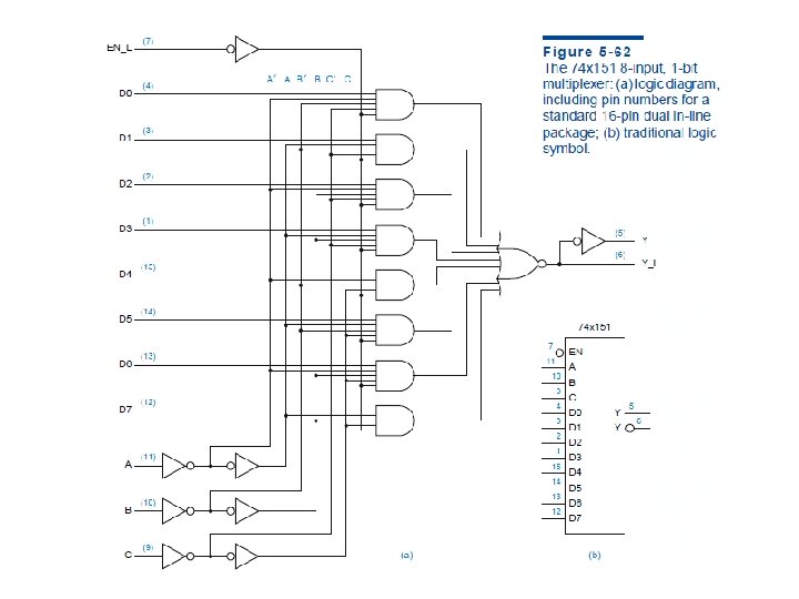
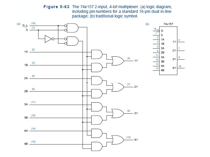
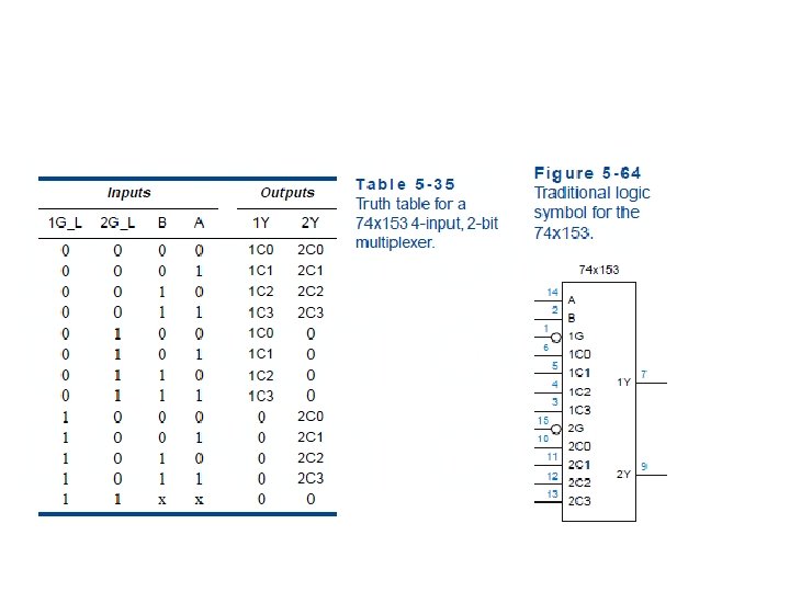
Standard MSI Multiplexers • The sizes of commercially available MSI multiplexers are limited by the number of pins available in an inexpensive IC package. • Commonly used muxes come in 16 -pin packages. Eg: IC 74 x 151

VHDL Program for a 8 -input, 1 -bit multiplexer Library ieee; Use ieee. std_logic_1164. all; Entity mux 8 in 1 bit is Port( EN_L: in std_logic; S: in std_logic_vector(2 downto 0); D: in std_logic_vector(7 downto 0); Y: out std_logic); End mux 8 in 1 bit; Architecture dataflow of mux 8 in 4 bit is Signal y 1: std_logic; Begin with S select Y 1<= D(7) when “ 111”, D(6) when “ 110”, D(5) when “ 101”, D(4) when “ 100”, D(3) when “ 011”, D(2) when “ 010”, D(1) when “ 001”, D(0) when “ 000”, ‘ 0’ when others; y<=y 1 when EN_L=‘ 0’ else ‘ 0’; End dataflow; Library ieee; Use ieee. std_logic_1164. all; Entity mux 8 in 1 bit is Port( EN_L: in std_logic; S: in std_logic_vector(2 downto 0); D: in std_logic_vector(7 downto 0); Y: out std_logic); End mux 8 in 1 bit; Architecture behav of mux 8 in 4 bit is Begin Process(EN_L, S, D) Begin Case S is When “ 111” => Y 1<= D(7) ; When “ 110” => Y 1<= D(6) ; When “ 101” => Y 1<= D(5) ; When “ 100” => Y 1<= D(4) ; When “ 011” => Y 1<= D(3) ; When “ 010” => Y 1<= D(2) ; When “ 001” => Y 1<= D(1) ; When “ 000” => Y 1<= D(0) ; when others => Y 1<=‘ 0’; End case; If(EN_L=‘ 0’) then Y<=Y 1; Else Y<=‘ 0’; End behav;

VHDL Program for 2 -input 4 -bit multiplexer Library ieee; Use ieee. std_logic_1164. all; Entity mux 2 in 4 bit is Port( EN_L, S: in std_logic; A, B: in std_logic_vector(4 downto 1); Y: out std_logic_Vector(4 downto 1)); End mux 2 in 4 bit; Architecture dataflow of mux 2 in 4 bit is Signal y 1: std_logic_vector(4 down to 1); Begin with S select Y 1<= A when ‘ 0’, B when ‘ 1’, “ 0000” when others; y<=y 1 when G_L=‘ 1’ else “ 0000”; End dataflow;

VHDL Program for 4 -input 2 -bit multiplexer Library ieee; Use ieee. std_logic_1164. all; Entity mux 4 in 2 bit is Port( G_L, S: in std_logic_vector(1 downto 0); C 1, C 2: in std_logic_vector(3 downto 0); Y: out std_logic_Vector(1 downto 0)); End mux 4 in 2 bit; Architecture dataflow of mux 2 in 4 bit is Signal y 1: std_logic_vector(1 downto 0); Begin Process(G_L, S, C 1, C 2) Begin If (G_L=“ 00”) then If (S=“ 00”) then Y 1(1)<= C 1(0); Y 1(0)<= C 2(0); Elsif (S=“ 01” ) then Y 1(1)<= C 1(1); Y 1(0)<= C 2(1); Elsif (S=“ 10” ) then Y 1(1)<= C 1(2); Y 1(0)<= C 2(2); Elsif (S=“ 11” ) then Y 1(1)<= C 1(3); Y 1(0)<= C 2(3); End if; Els if(G_L=“ 01” ) then If (S=“ 00”) then Y 1(1)<= C 1(0); Y 1(0)<= ‘ 0’; Elsif (S=“ 01” ) then Y 1(1)<= C 1(1); Y 1(0)<= ‘ 0’; Elsif (S=“ 10” ) then Y 1(1)<= C 1(2); Y 1(0)<= ‘ 0’; Elsif (S=“ 11” ) then Y 1(1)<= C 1(3); Y 1(0)<= ‘ 0’; End if; Els if(G_L=“ 10” ) then If (S=“ 00”) then Y 1(1)<= ‘ 0’; Y 1(0)<= C 2(0); Elsif (S=“ 01” ) then Y 1(1)<= ‘ 0’; Y 1(0)<= C 2(1); Elsif (S=“ 10” ) then Y 1(1)<= ‘ 0’; Y 1(0)<= C 2(2); Elsif (S=“ 11” ) then Y 1(1)<= ‘ 0’; Y 1(0)<= C 2(3); End if; Elsif (G_L=“ 11”) then Y 1=“ 00”; end if; End process; End dataflow;

Library ieee; Use ieee. std_logic_1164. all; Entity mux 32 in is Port( XEN_L: in std_logic; X: in std_logic_vector(31 downto 0); Y: out std_logic); End mux 4 in 2 bit; Architecture structural of mux 32 in is Component IC 74139 is Port(G_L: in std_logic; A, B: in std_logic_vector(1 downto 0); Y 1, y 2: out std_logic_vector(3 downto 0)); End component;

VHDL Program for 32 -bit multiplexer Component IC 74 x 151 is Port(EN_L: in std_logic; S: in std_logic_vector(2 downto 0); D: in std_logic_vector(7 downto 0); Y_L: out std_logic); End component; Component IC 74 x 20 is Port(D_L: in std_logic_vector(3 downto 0); Y: out std_logic); End component; Signal Z_L, Z 1_L, Z 2_L: std_logic_vector(3 downto 0); Begin U 1: IC 74139 port map(XEN_L, S(3), ‘ 0’, S(4), ‘ 0’, Z_L, Z 1_L ); U 2: IC 74 x 151 port map(Z_L(0), S(2), S(1), S(0), X(7 downto 0), Z 2_L(0)); U 3: IC 74 x 151 port map(Z_L(1), S(2), S(1), S(0), X(15 downto 8), Z 2_L(1)); U 4: IC 74 x 151 port map(Z_L(2), S(2), S(1), S(0), X(23 downto 16), Z 2_L(2)); U 5: IC 74 x 151 port map(Z_L(3), S(2), S(1), S(0), X(31 downto 24), Z 2_L(3)); U 6: IC 74 x 20 port map(Z 2_L, Y); End structural;

Code Converters

Binary Codes • A symbolic representation of data/ information is called code. • The base or radix of the binary number is 2. It has two independent symbols. The symbols used are 0 and 1. • A binary digit is called as a bit. A binary number consists of sequence of bits, each of which is either a 0 or 1. • Each bit carries a weight based on its position relative to the binary point. • The weight of each bit position is one power of 2 greater than the weight of the position to its immediate right. • e g. , of binary number is 100011 which is equivalent to decimal number 35.

BCD Codes • Numeric codes represent numeric information i. e. only numbers as a series of 0’s and 1’s. • Numeric codes used to represent decimal digits are called Binary Coded Decimal (BCD) codes. • A BCD code is one, in which the digits of a decimal number are encoded-one at a time into group of four binary digits. • There a large number of BCD codes in order to represent decimal digits 0, 1, 2 … 9, it is necessary to use a sequence of at least four binary digits. • Such a sequence of binary digits which represents a decimal digit is called code word.

Gray Codes • It is a non-weighted code; therefore, it is not a suitable for arithmetic operations. • It is a cyclic code because successive code words in this code differ in one bit position only i. e. it is a unit distance code. Applications of Gray Code: • In instrumentation and data acquisition systems, where linear or angular displacement is measured. • In shaft encoders, input-output devices, A/D converters and the other peripheral equipment.

Excess-3 code • It is a non-weighted code. It is also a selfcomplementing BCD code used in decimal arithmetic units. • The Excess-3 code for the decimal number is performed in the same manner as BCD except that decimal number 3 is added to the each decimal unit before encoding it to binary.

Code Converters • The availability of a large variety of codes for the same discrete elements of information results in the use of different codes by different digital systems. • It is some time necessary to use the output of one system as the input to the other. • The conversion circuit must be inserted between the two systems if each uses different codes for the same information. • A code converter is a circuit that makes the two systems compatible even though each uses the different code.

Binary to Gray code Binary Gray Decimal No D C B A G 3 G 2 G 1 G 0 0 0 0 0 1 2 0 0 1 0 0 0 1 1 3 0 0 1 1 0 0 1 0 4 0 1 0 0 0 1 1 0 5 0 1 0 1 1 1 6 0 1 1 0 0 1 7 0 1 1 1 0 8 1 0 0 0 1 1 0 0 9 1 0 0 1 1 1 0 1 10 1 0 1 1 11 1 0 12 1 1 0 0 1 0 13 1 1 0 1 1 14 1 1 1 0 0 1 15 1 1 1 0 0 0

Output Equations and Logic Diagram

VHDL Program Library ieee; Use ieee. std_logic_1164. all; Entity binary 2 gray is Port( A, B, C, D: in std_logic; G: out std_logic_vector(3 downto 0)); End binary 2 gray; Architecture dataflow of binary 2 gray is Begin G(0)<=B xor A; G(1)<= C xor B; G(2)<= D xor C; G(3)<= D; End dataflow;

Gray to Binary Converter Gray Decimal No Binary G 3 G 2 G 1 G 0 D C B A 0 1 2 3 4 5 6 7 8 9 0 0 0 0 1 1 1 0 0 1 1 0 1 0 0 0 1 1 0 0 0 0 1 1 0 0 1 1 0 0 0 1 0 1 0 1 1 1 1 1 0 11 1 0 1 1 12 1 0 1 1 0 0 13 1 0 1 14 1 0 0 1 1 0 15 1 0 0 0 1 1

Equations and Logic Diagram

VHDL Program Library ieee; Use ieee. std_logic_1164. all; Entity gray 2 binary is Port( G: in std_logic_vector(3 downto 0); A, B, C, D: out std_logic); End gary 2 binary; Architecture dataflow of gray 2 binary is Begin A<=(G(3) xor G(2) ) xor (G(1) xor G(0)); B<= G(3) xor G(2) xor G(1); C<= G(3) xor G(2); D<= G(3); End dataflow;

BCD to Excess-3 Converter Decimal Digit BCD Excess-3 B 2 B 1 B 0 E 3 E 2 E 1 E 0 0 0 0 1 1 1 0 0 0 1 0 0 2 0 0 1 0 1 3 0 0 1 1 0 4 0 1 0 0 0 1 1 0 5 0 1 1 0 0 1 6 0 1 1 0 0 1 7 0 1 1 0 1 0 8 1 0 0 0 1 0 9 1 0 0 1 1 1 0 1 z = D y = CD+C’D’=CD(C+D)’ x = B’C+B’D+BC’D’= B’(C+D) +BC’D’ x = B’(C+D) +B(C+D)’ w= A+BC+BD=A+B(C+D)

Logic Diagram

VHDL Program Library ieee; Use ieee. std_logic_1164. all; Entity bcd 2 excess 3 is Port( A, B, C, D: in std_logic; W, X, Y, Z: out std_logic); End bcd 2 excess 3; Architecture dataflow of bcd 2 excess 3 is Begin Z<=D; Y<= (C and D) and (not(C or D)); X<=((not B) and (C or D)) or (B and (not(C or D))); W<=A or (B and (C or D)); End dataflow;

Excess-3 to BCD Converter Decimal Digit 0 1 2 3 4 5 6 7 8 9 E 3 0 0 0 1 1 1 Excess-3 E 2 E 1 0 1 0 1 1 0 0 0 1 1 0 BCD E 0 1 0 0 1 B 3 0 0 0 0 1 1 B 2 0 0 1 1 0 0 B 1 0 0 1 1 0 0 B 0 0 1 0 1 0 1

Logic Diagram

VHDL Program Library ieee; Use ieee. std_logic_1164. all; Entity excess 3 tobcd is Port( E: in std_logic_vector(3 downto 0); B: out std_logic_vector(3 downto 0)); End excess 3 tobcd; Architecture dataflow of excess 3 tobcd is Begin B(0)<=E(0) xor ((not E(1)) and (not(E(2) and E(3))); B(1)<=E(1) xor (not(E(2) and E(3))); B(2)<=E(2) xor E(3); B(3)<=E(3) xor ‘ 1’; End dataflow;

EXCLUSIVE OR Gates and Parity Circuits
 gate is a")
EXCLUSIVE OR and EXCLUSIVE NOR Gates • An Exclusive OR (XOR) gate is a 2 -input gate whose output is 1 if exactly one of its inputs is 1. • An XOR gate produces a 1 output if its inputs are different. • An Exclusive NOR (XNOR) or Equivalence gate is just the opposite—it produces a 1 output if its inputs are the same.
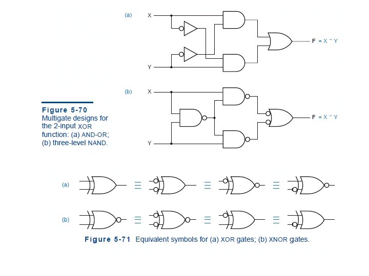

• Four XOR gates are provided in a single 14 -pin SSI IC 74 x 86. • New SSI logic families do not offer XNOR gates, although they are readily available in FPGA and ASIC libraries and as primitives in HDLs.

Cascading XOR Gates

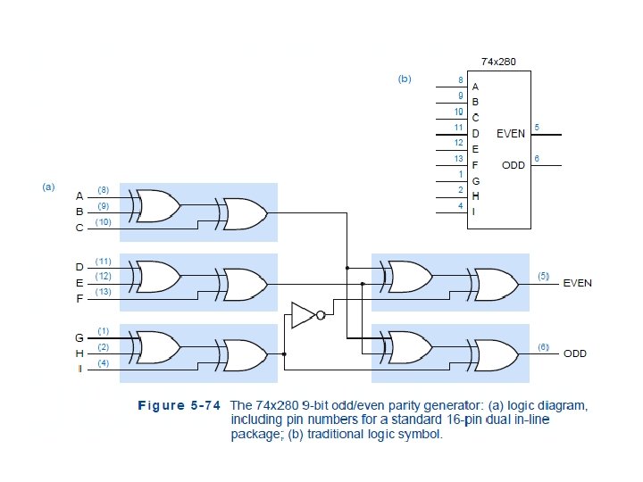
Parity Circuits • Parity Circuits • n XOR gates may be cascaded to form a circuit with n + 1 inputs and a single output. This is called an odd-parity circuit, because its output is 1 if an odd number of its inputs are 1. The circuit in (b) is also an odd parity circuit, but it’s faster because its gates are arranged in a tree-like structure. • If the output of either circuit is inverted, we get an even-parity circuit, whose output is 1 if an even number of its inputs are 1. • The 74 x 280 9 -Bit Parity Generator • Rather than build a multibit parity circuit with discrete XOR gates, it is more economical to put all of the XORs in a single MSI package with just the primary inputs and outputs available at the external pins. • Eg: The 74 x 280 9 -bit parity generator, has nine inputs and two outputs that indicate whether an even or odd number of inputs are 1. • Parity-Checking Applications • The error-detecting codes that use an extra bit, called a parity bit, to detect errors in the transmission and storage of data. In an even parity code, the parity bit is chosen so that the total number of 1 bits in a code word is even. • Parity circuits like the 74 x 280 are used both to generate the correct value of the parity bit when a code word is stored or transmitted, and to check the parity bit when a code word is retrieved or received.

VHDL Program for 9 -input Parity Checker library IEEE; use IEEE. std_logic_1164. all; entity parity 9 is port ( I: in STD_LOGIC_VECTOR (1 to 9); EVEN, ODD: out STD_LOGIC ); end parity 9; process (I) variable p : STD_LOGIC; variable j : INTEGER; Begin p : = I(1); for j in 2 to 9 loop if I(j) = '1' then p : = not p; end if; end loop; ODD <= p; EVEN <= not p; end process; architecture parity 9 p of parity 9 is Begin end parity 9 p;

VHDL Program in Structural Mode library IEEE; use IEEE. std_logic_1164. all; signal Y 1, Y 2, Y 3 N: STD_LOGIC; entity V 74 x 280 is port ( I: in STD_LOGIC_VECTOR (1 to 9); EVEN, ODD: out STD_LOGIC ); end V 74 x 280; begin U 1: vxor 3 port map (I(1), I(2), I(3), Y 1); U 2: vxor 3 port map (I(4), I(5), I(6), Y 2); U 3: vxor 3 port map (I(7), I(8), I(9), Y 3); Y 3 N <= not Y 3; U 4: vxor 3 port map (Y 1, Y 2, Y 3, ODD); U 5: vxor 3 port map (Y 1, Y 2, Y 3 N, EVEN); architecture V 74 x 280 s of V 74 x 280 is end V 74 x 280 s; component vxor 3 port (A, B, C: in STD_LOGIC; Y: out STD_LOGIC); end component;

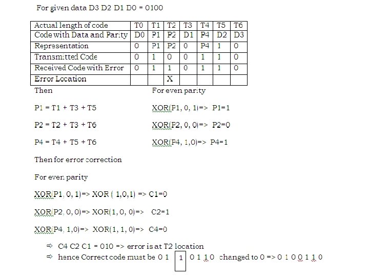
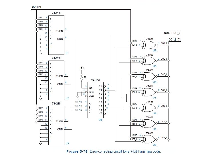
Error Correcting Circuit for 7 -bit Hamming Code • Hamming Codes are a family of linear error-correcting codes that generalize the hamming(7, 4) code. • Hamming codes can detect up to two-bit errors or correct one-bit errors without detection of uncorrected errors. • The simple parity code cannot correct errors, and can detect only an odd number of bits in error. • Hamming codes are perfect codes, i. e. , they achieve the highest possible rate for codes with their block length and minimum distance 3. • Eg: let databits = 0100 = d 3 d 2 d 1 d 0 • Parity bits = P 3 P 2 P 1 3 Bit String 000 001 010 011 100 101 110 111 Parity Bit 0 1 1 0 0 1

Comparators

Comparator Structure • EXCLUSIVE OR and EXCLUSIVE NOR gates may be viewed as 1 -bit comparators. • The 74 x 86 XOR gate can be used as a 1 -bit comparator. The active-high output, DIFF, is asserted if the inputs are different. • Given enough XOR gates and wide enough OR gates, comparators with any number of input bits can be built.

Iterative Circuits • The circuit contains n identical modules, each of which has both primary inputs and outputs and cascading inputs and outputs. • The leftmost cascading inputs are called boundary inputs and are connected to fixed logic values in most iterative circuits. • The rightmost cascading outputs are called boundary outputs and usually provide important information. • Iterative circuits are well suited to problems that can be solved by a simple iterative algorithm: 1. Set C 0 to its initial value and set i to 0. 2. Use Ci and PIi to determine the values of POi and Ci+1. 3. Increment i. 4. If i < n, go to step 2. • In an iterative circuit, the loop of steps 2– 4 is “unwound” by providing a separate combinational circuit that performs step 2 for each value of i. • Eg: The 74 x 85 4 -bit comparator and the 74 x 283 4 -bit adder are MSI circuits that can be used as the individual modules in a larger iterative circuit.

Iterative Circuits

An Iterative Comparator Circuit • Two n-bit values X and Y can be compared one bit at a time using a single bit EQi at each step to keep track of whether all of the bit-pairs have been equal so far: 1. Set EQ 0 to 1 and set i to 0. 2. If EQi is 1 and Xi and Yi are equal, set EQi + 1 to 1. Else set EQi+1 to 0. 3. Increment i. 4. If i < n, go to step 2. • saves cost but delay increases due to ripple of cascading signals.

An MSI IC 74 x 85 4 - bit comparator has cascading inputs ALTBIN, AEQBIN, AGTBIN

MSI Comparator
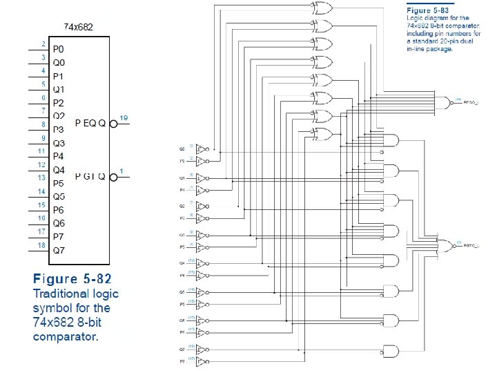

Comparator Conditions • Derived from IC 74 x 682 and 74 xx Series

VHDL Program library IEEE; use IEEE. std_logic_1164. all; entity vcompare is port ( A, B: in STD_LOGIC_VECTOR (7 downto 0); EQ, NE, GT, GE, LT, LE: out STD_LOGIC ); end vcompare; architecture vcompare_arch of vcompare is Begin process (A, B) Begin EQ <= '0'; NE <= '0'; GT <= '0'; GE <= '0'; LT <= '0'; LE <= '0'; if A = B then EQ <= '1'; end if; if A /= B then NE <= '1'; end if; if A > B then GT <= '1'; end if; if A >= B then GE <= '1'; end if; if A < B then LT <= '1'; end if; if A <= B then LE <= '1'; end if; end process; end vcompare_arch;

VHDL Program library IEEE; use IEEE. std_logic_1164. all; use IEEE. std_logic_arith. all; entity vcompa is port ( A, B: in UNSIGNED (7 downto 0); C: in SIGNED (7 downto 0); D: in STD_LOGIC_VECTOR (7 downto 0); A_LT_B, B_GE_C, A_EQ_C, C_NEG, D_BIG, D_NEG: out STD_LOGIC ); end vcompa; architecture vcompa_arch of vcompa is begin process (A, B, C, D) Begin A_LT_B <= '0'; B_GE_C <= '0'; A_EQ_C <= '0'; C_NEG <= '0'; D_BIG <= '0'; D_NEG <= '0'; if A < B then A_LT_B <= '1'; end if; if B >= C then B_GE_C <= '1'; end if; if A = C then A_EQ_C <= '1'; end if; if C < 0 then C_NEG <= '1'; end if; if UNSIGNED(D) > 200 then D_BIG <= '1'; end if; if SIGNED(D) < 0 then D_NEG <= '1'; end if; end process; end vcompa_arch;

Multipliers

Combinational Multipliers • Multipliers can be designed using combinational circuits such as adders and registers. • Basic Multipliers use the shift-and-add algorithm emulates the way that we do paper-and-pencil multiplication of decimal numbers, there is nothing inherently “sequential” or “time dependent” about multiplication.

VHDL Program
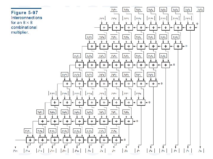

Sequential Multipliers • Sequential multipliers use a single adder and a register to accumulate the partial products. The partial-product register is initialized to the first product component, and for an nxn-bit multiplication, n-1 steps are taken and the adder is used n-1 times, once for each of the remaining n-1 product components to be added to the partial-product register. • Sequential multipliers use carry-save addition to speed up multiplication. The idea is to break the carry chain of the ripple adder to shorten the delay of each addition i. e. , by applying the carry output from bit i during step j to the carry input for bit i+1 during the next step, j+1. • After the last product component is added, one more step is needed in which the carries are hooked up in the usual way and allowed to ripple from the least to the most significant bit. • Although this adder uses exactly the same amount of logic as the previous one (64 2 -input AND gates and 56 full adders), its propagation delay is substantially shorter. • Its worst-case delay path goes through only 14 full adders. The delay can be further improved by using a carry look ahead adder for the last row. • The regular structure of combinational multipliers make them ideal for VLSI and ASIC realization. The importance of fast multiplication in microprocessors, digital video, and many other applications has led to much study and development of even better structures and circuits for combinational multipliers.
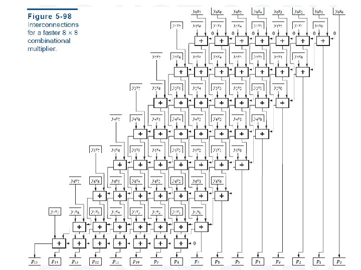

8 x 8 Multiplier

VHDL Program library IEEE; use IEEE. std_logic_1164. all; entity vmul 8 x 8 p is port ( X: in STD_LOGIC_VECTOR (7 downto 0); Y: in STD_LOGIC_VECTOR (7 downto 0); P: out STD_LOGIC_VECTOR (15 downto 0) ); end vmul 8 x 8 p; architecture vmul 8 x 8 p_arch of vmul 8 x 8 p is function MAJ (I 1, I 2, I 3: STD_LOGIC) return STD_LOGIC is Begin return ((I 1 and I 2) or (I 1 and I 3) or (I 2 and I 3)); end MAJ; Begin process (X, Y) type array 8 x 8 is array (0 to 7) of STD_LOGIC_VECTOR (7 downto 0); variable PC: array 8 x 8; -- product component bits variable PCS: array 8 x 8; -- full-adder sum bits variable PCC: array 8 x 8; -- full-adder carry output bits variable RAS, RAC: STD_LOGIC_VECTOR (7 downto 0); -- ripple adder sum begin -- and carry bits for i in 0 to 7 loop for j in 0 to 7 loop PC(i)(j) : = Y(i) and X(j); -- compute product component bits end loop; for j in 0 to 7 loop PCS(0)(j) : = PC(0)(j); -- initialize first-row "virtual" PCC(0)(j) : = '0'; -- adders (not shown in figure) end loop; for i in 1 to 7 loop -- do all full adders except last row for j in 0 to 6 loop PCS(i)(j) : = PC(i)(j) xor PCS(i-1)(j+1) xor PCC(i-1)(j); PCC(i)(j) : = MAJ(PC(i)(j), PCS(i-1)(j+1), PCC(i-1)(j)); PCS(i)(7) : = PC(i)(7); -- leftmost "virtual" adder sum output end loop; RAC(0) : = '0'; for i in 0 to 6 loop -- final ripple adder RAS(i) : = PCS(7)(i+1) xor PCC(7)(i) xor RAC(i); RAC(i+1) : = MAJ(PCS(7)(i+1), PCC(7)(i), RAC(i)); end loop; for i in 0 to 7 loop P(i) <= PCS(i)(0); -- first 8 product bits from full-adder sums end loop; for i in 8 to 14 loop P(i) <= RAS(i-8); -- next 7 bits from ripple-adder sums end loop; P(15) <= RAC(7); -- last bit from ripple-adder carry end process; end vmul 8 x 8 p_arch;

Half Adders and Full Adders

VHDL Program HALFADDER Library ieee; Use ieee. std_logic_1164. all; Entity ha is Port(a, b: in std_logic; S, C: out std_logic); End ha; Architecture dataflow of ha is Begin S<=a xor b; C<=a and b; End dataflow; FULL ADDER Library ieee; Use ieee. std_logic_1164. all; Entity fa is Port(a, b, c: in std_logic; S, Cout: out std_logic); End ha; Architecture dataflow of ha is Begin S<=(a xor b) xor c; Cout<=((a and b) or ( b and C)) or ( c and a); End dataflow;

Ripple Adders • A ripple adder is slow, since in the worst case a carry must propagate from the least significant full adder to the most significant one. • This occurs if, for example, one addend is 11 … 11 and the other is 00 … 01. • Assuming that all of the addend bits are presented simultaneously, the total worst-case delay is

VHDL Program for ripple carry adder Library ieee; Use ieee. std_logic_1164. all; Entity rca is Port(a, b: in std_logic_vector(3 downto 0); Cin: in std_logic; S: out std_logic_vector(3 downto 0); Cout: out std_logic); End ha; Architecture structural of rca is Component fa is Port(a, b, c: in std_logic; S, Cout: out std_logic); End component; Signal c: std_logic_vector(3 downto 0); Begin U 1: fa port map(a(0), b(0), cin, S(0), C(0)); U 2: fa port map(a(1), b(1), cin, S(1), C(1)); U 3: fa port map(a(2), b(2), cin, S(2), C(2)); U 4: fa port map(a(3), b(3), cin, S(3), Cout); End dataflow;

Subtractor • A full subtractor handles one bit of the binary subtraction algorithm, having input bits X (minuend), Y (subtrahend), and BIN (borrow in), and output bits D (difference) and BOUT (borrow out). (or)

Subtractor Design

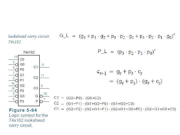
Carry Look Ahead Adder

VHDL Program for MSI Adders Library ieee; Use ieee. std_logic_1164. all; Entity CLA is Port(a, b: in std_logic_vector(3 downto 0); Cin: in std_logic; S: out std_logic_vector(3 downto 0); Cout: out std_logic); End CLA; Architecture dataflow of CLA is Signal g, p, c: std_logic_vector(3 downto 0); Variable i: integer; Process(a, b, cin) Begin S(0)<=(a(0) xor b(0)) xor Cin; For I in 0 to 3 loop g(i)<= a(i) and b(i); P(i)<= a(i) or b(i); C(i+1)<= g(i) or ( p(i) and c(i)); End loop; For I in 1 to 3 loop S(i)<= (a(i) xor b(i)) xor c(i); End loop; Cout<=c(3); Begin End process; End dataflow;

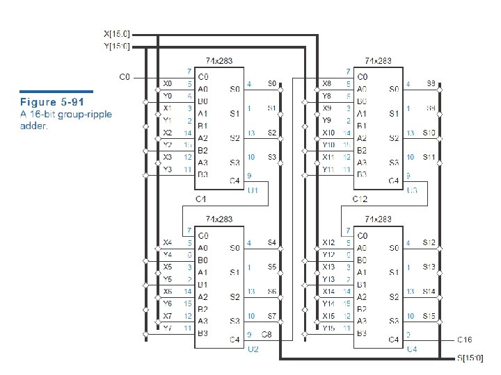
MSI Adders

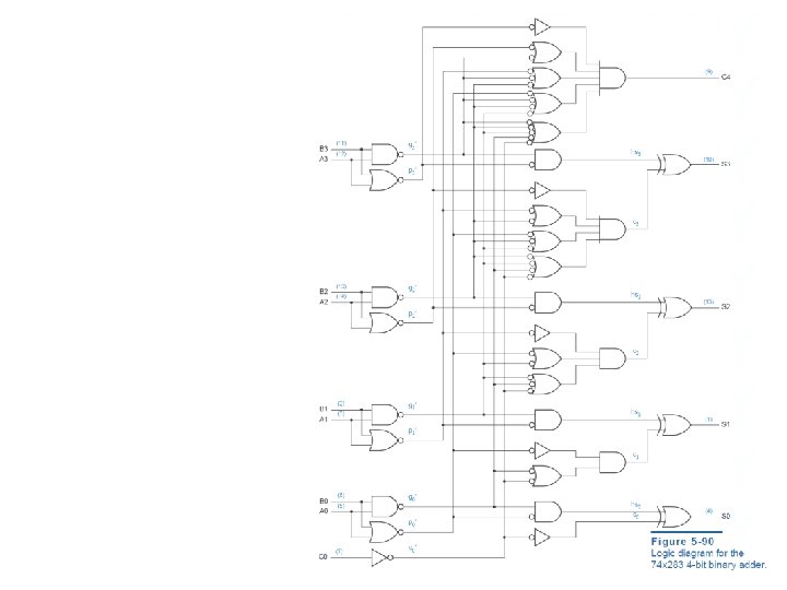
MSI Adders

VHDL Program for MSI Adders Library ieee; Use ieee. std_logic_1164. all; Entity add 74 x 283 is Port(a, b: in std_logic_vector(3 downto 0); Cin: in std_logic; S: out std_logic_vector(3 downto 0); Cout: out std_logic); End add 74 x 283; Architecture structural of add 74 x 283 is Begin

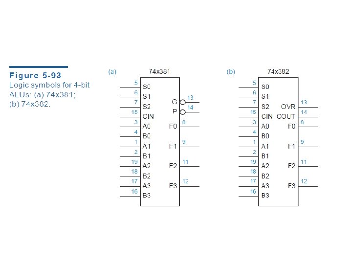
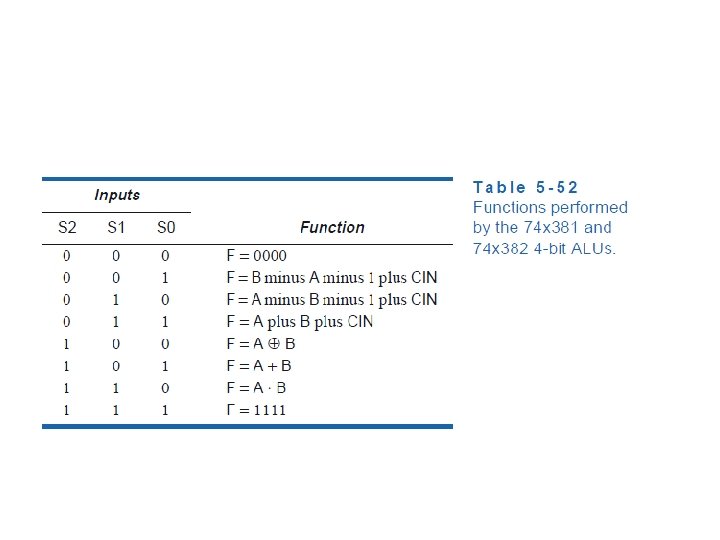
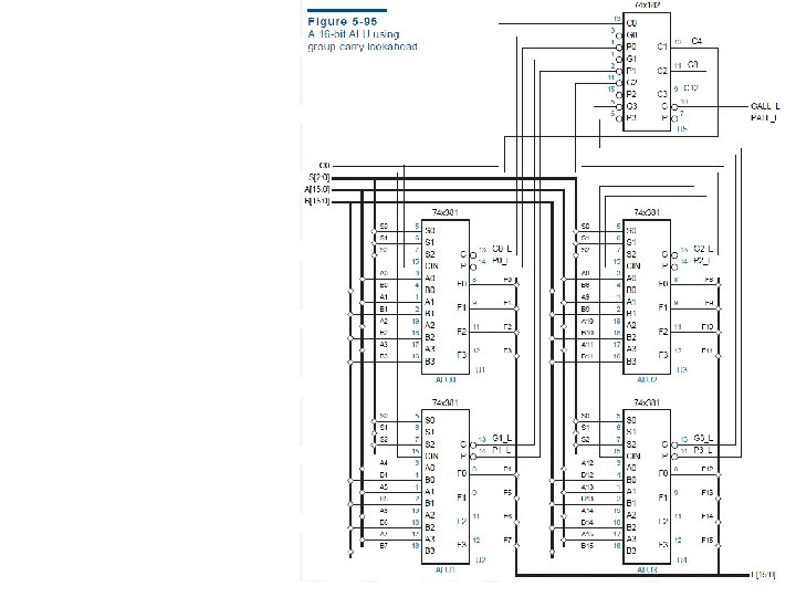
ALU

VHDL program for adding and subtracting 8 -bit integers of various types library IEEE; use IEEE. std_logic_1164. all; use IEEE. std_logic_arith. all; entity vadd is port ( A, B: in UNSIGNED (7 downto 0); C: in SIGNED (7 downto 0); D: in STD_LOGIC_VECTOR (7 downto 0); S: out UNSIGNED (8 downto 0); T: out SIGNED (8 downto 0); U: out SIGNED (7 downto 0); V: out STD_LOGIC_VECTOR (8 downto 0) ); end vadd; architecture vadd_arch of vadd is begin S <= ('0' & A) + ('0' & B); T <= A + C; U <= C + SIGNED(D); V <= C - UNSIGNED(D); end vadd_arch;
- Slides: 113