Chapter 5 COMBINATIONAL LOGIC ANALYSIS Basic combinational logic
Chapter 5 COMBINATIONAL LOGIC ANALYSIS
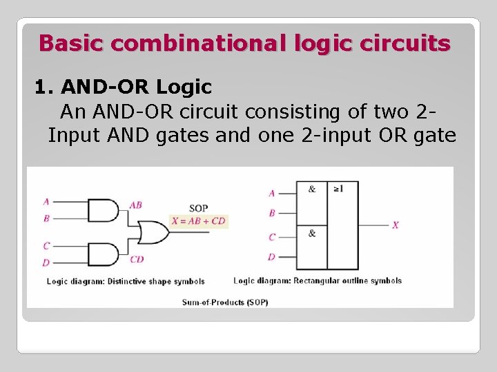
Basic combinational logic circuits 1. AND-OR Logic An AND-OR circuit consisting of two 2 Input AND gates and one 2 -input OR gate
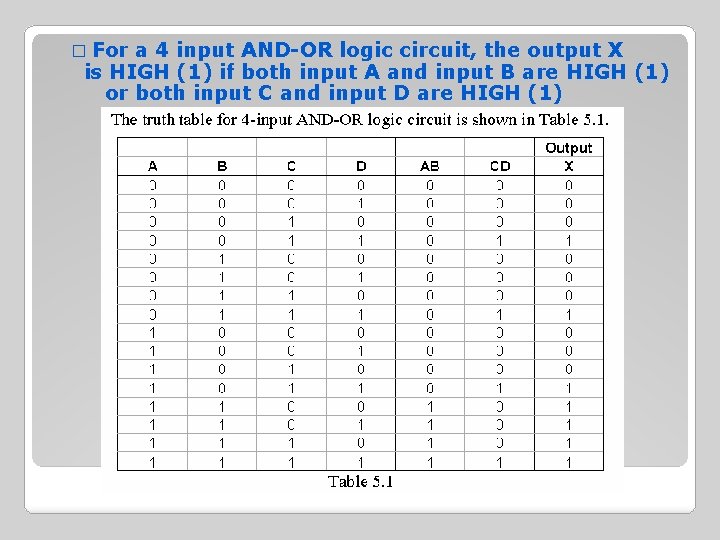
� For a 4 input AND-OR logic circuit, the output X is HIGH (1) if both input A and input B are HIGH (1) or both input C and input D are HIGH (1)
EXAMPLE In a certain chemical processing plant, a liquid chemical is used in a manufacturing process. The chemical is stored in 3 different tanks. A level sensor in each tank produces HIGH voltage when the level of chemical in the tank drops below a specified point. i) ii) Design a circuit that monitors the chemical level in each tank and indicates when the level in any two of the tanks drops below the specified point. Write the Boolean SOP expression for the AND-OR logic circuit design in (i).
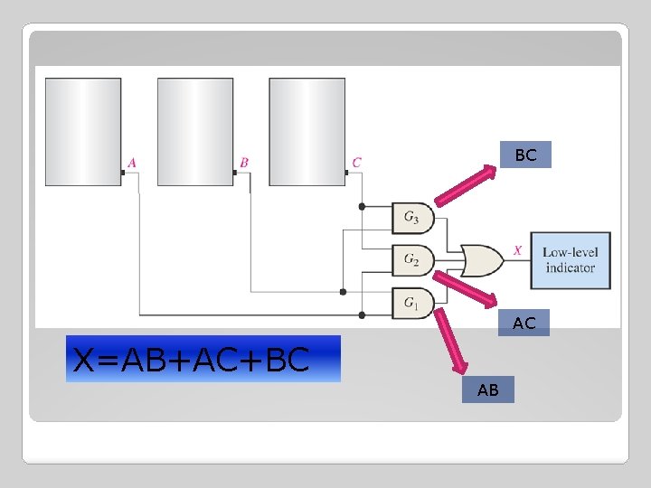
BC AC X=AB+AC+BC AB
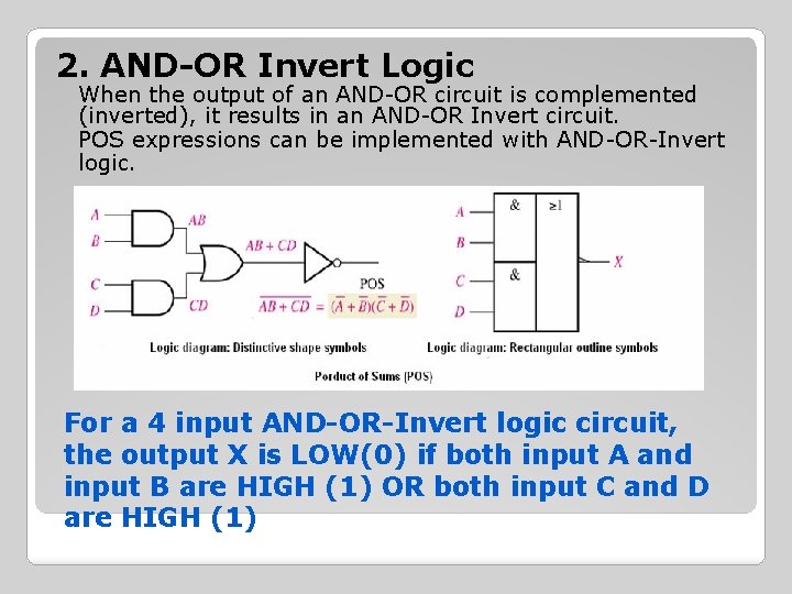
2. AND-OR Invert Logic When the output of an AND-OR circuit is complemented (inverted), it results in an AND-OR Invert circuit. POS expressions can be implemented with AND-OR-Invert logic. For a 4 input AND-OR-Invert logic circuit, the output X is LOW(0) if both input A and input B are HIGH (1) OR both input C and D are HIGH (1)
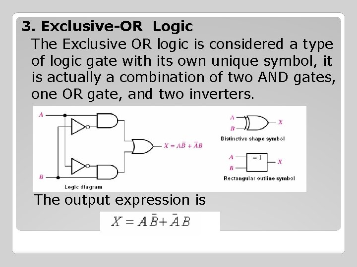
3. Exclusive-OR Logic The Exclusive OR logic is considered a type of logic gate with its own unique symbol, it is actually a combination of two AND gates, one OR gate, and two inverters. The output expression is
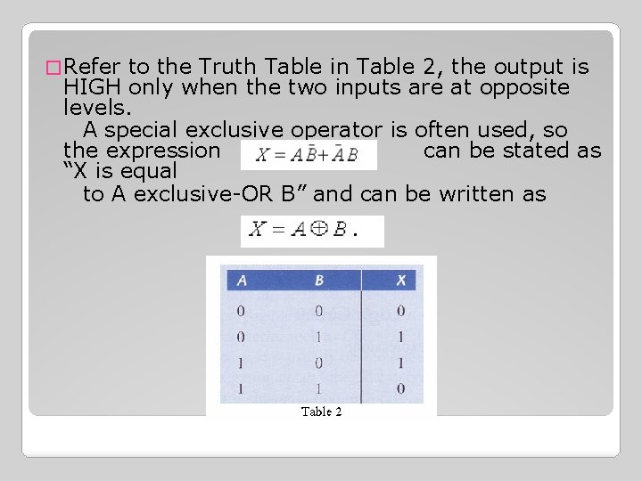
� Refer to the Truth Table in Table 2, the output is HIGH only when the two inputs are at opposite levels. A special exclusive operator is often used, so the expression can be stated as “X is equal to A exclusive-OR B” and can be written as
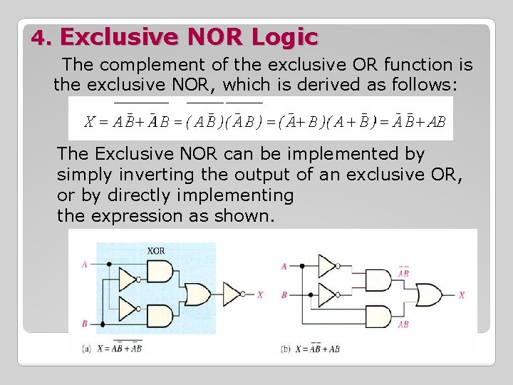
4. Exclusive NOR Logic The complement of the exclusive OR function is the exclusive NOR, which is derived as follows: The Exclusive NOR can be implemented by simply inverting the output of an exclusive OR, or by directly implementing the expression as shown.
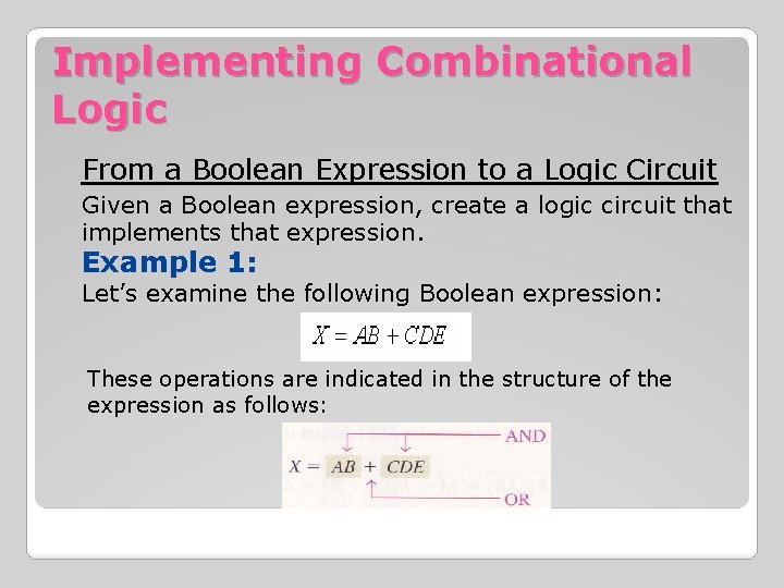
Implementing Combinational Logic From a Boolean Expression to a Logic Circuit Given a Boolean expression, create a logic circuit that implements that expression. Example 1: Let’s examine the following Boolean expression: These operations are indicated in the structure of the expression as follows:
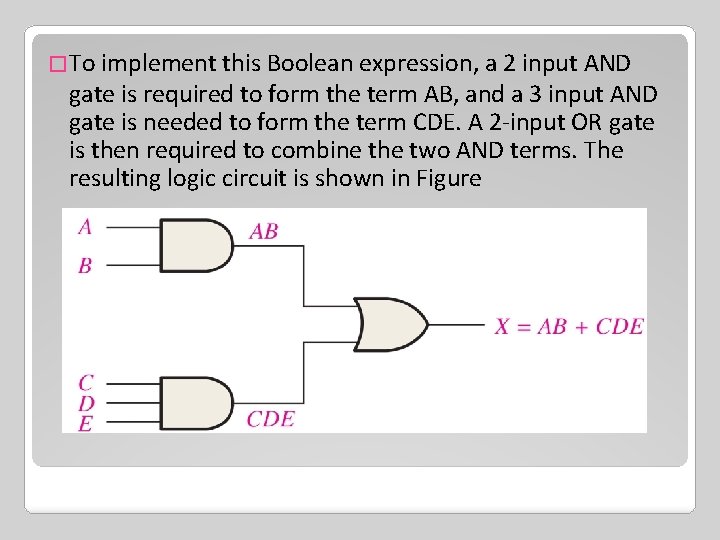
�To implement this Boolean expression, a 2 input AND gate is required to form the term AB, and a 3 input AND gate is needed to form the term CDE. A 2 -input OR gate is then required to combine the two AND terms. The resulting logic circuit is shown in Figure
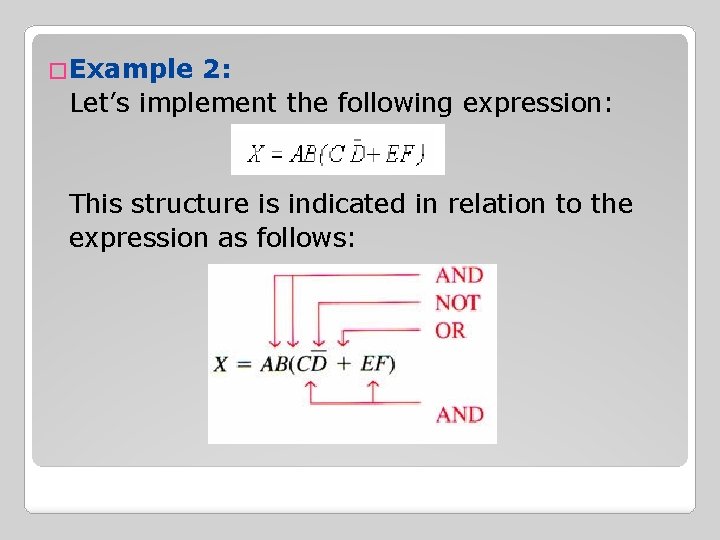
�Example 2: Let’s implement the following expression: This structure is indicated in relation to the expression as follows:
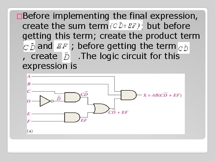
�Before implementing the final expression, create the sum term but before getting this term; create the product term and ; before getting the term , create. The logic circuit for this expression is
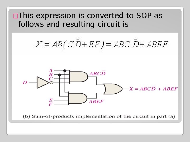
�This expression is converted to SOP as follows and resulting circuit is
�From a Truth Table to a Logic Circuit Given a truth table, create a logic circuit that implements that table. ◦ Step 1: Write the SOP expression from the truth table ◦ Step 2: Then implement the logic circuit
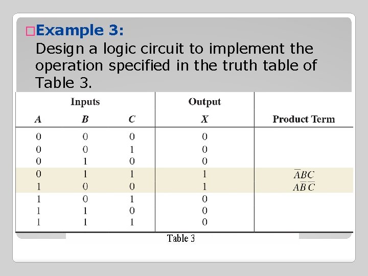
�Example 3: Design a logic circuit to implement the operation specified in the truth table of Table 3.
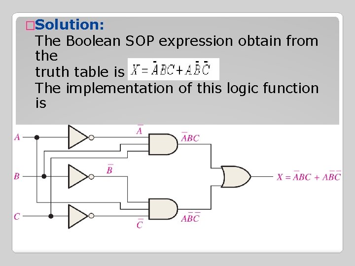
�Solution: The Boolean SOP expression obtain from the truth table is The implementation of this logic function is
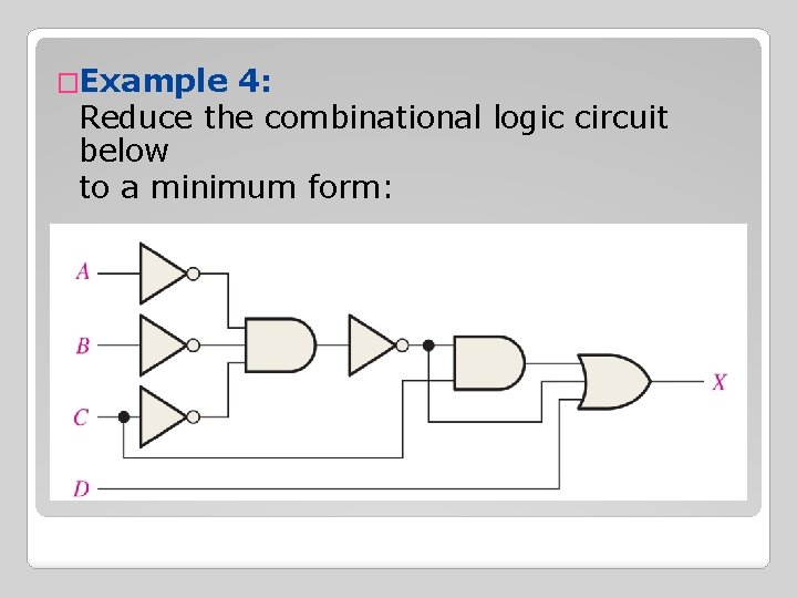
�Example 4: Reduce the combinational logic circuit below to a minimum form:

ANSWER:
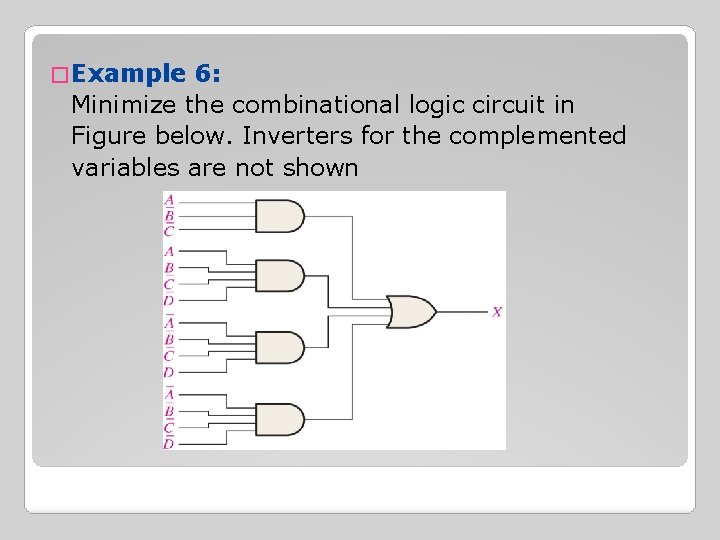
� Example 6: Minimize the combinational logic circuit in Figure below. Inverters for the complemented variables are not shown
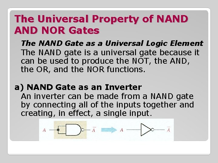
The Universal Property of NAND NOR Gates The NAND Gate as a Universal Logic Element The NAND gate is a universal gate because it can be used to produce the NOT, the AND, the OR, and the NOR functions. a) NAND Gate as an Inverter An inverter can be made from a NAND gate by connecting all of the inputs together and creating, in effect, a single input.
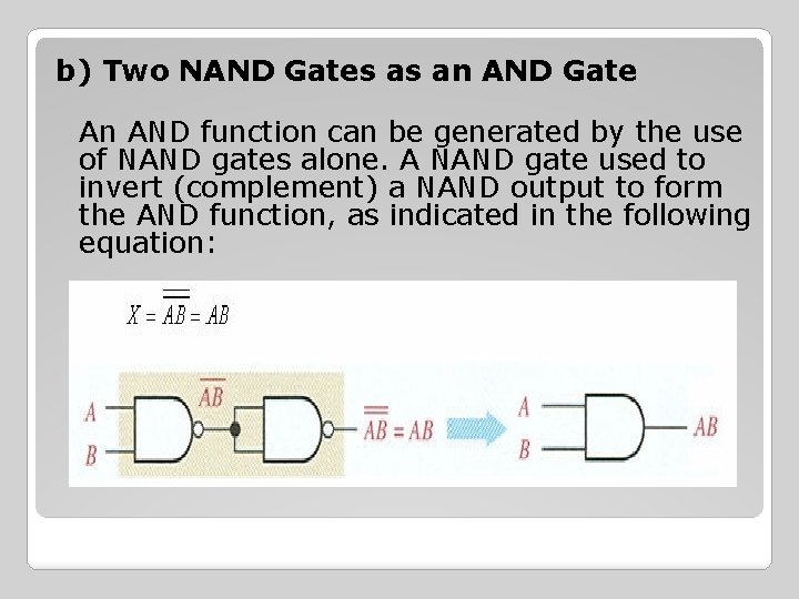
b) Two NAND Gates as an AND Gate An AND function can be generated by the use of NAND gates alone. A NAND gate used to invert (complement) a NAND output to form the AND function, as indicated in the following equation:
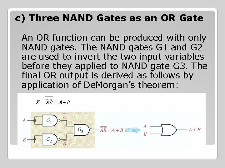
c) Three NAND Gates as an OR Gate An OR function can be produced with only NAND gates. The NAND gates G 1 and G 2 are used to invert the two input variables before they applied to NAND gate G 3. The final OR output is derived as follows by application of De. Morgan’s theorem:
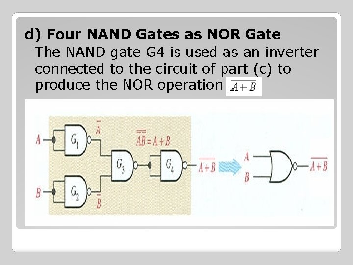
d) Four NAND Gates as NOR Gate The NAND gate G 4 is used as an inverter connected to the circuit of part (c) to produce the NOR operation
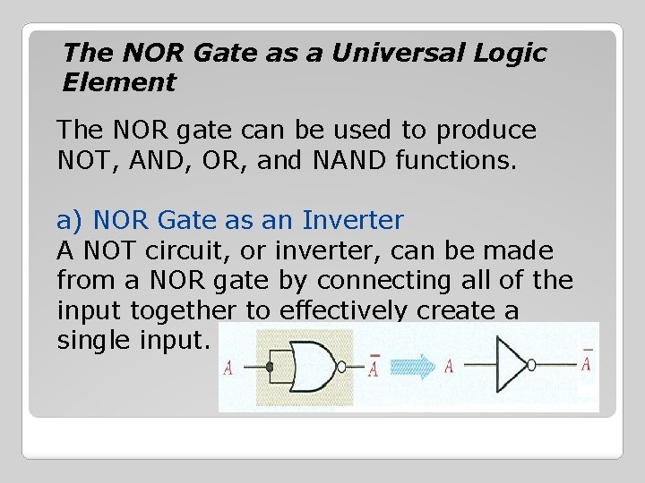
The NOR Gate as a Universal Logic Element The NOR gate can be used to produce NOT, AND, OR, and NAND functions. a) NOR Gate as an Inverter A NOT circuit, or inverter, can be made from a NOR gate by connecting all of the input together to effectively create a single input.
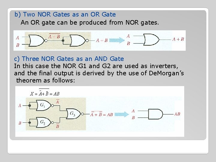
b) Two NOR Gates as an OR Gate An OR gate can be produced from NOR gates. c) Three NOR Gates as an AND Gate In this case the NOR G 1 and G 2 are used as inverters, and the final output is derived by the use of De. Morgan’s theorem as follows:
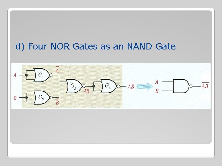
d) Four NOR Gates as an NAND Gate
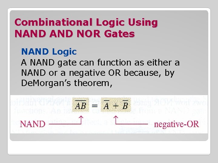
Combinational Logic Using NAND NOR Gates NAND Logic A NAND gate can function as either a NAND or a negative OR because, by De. Morgan’s theorem,
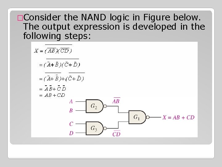
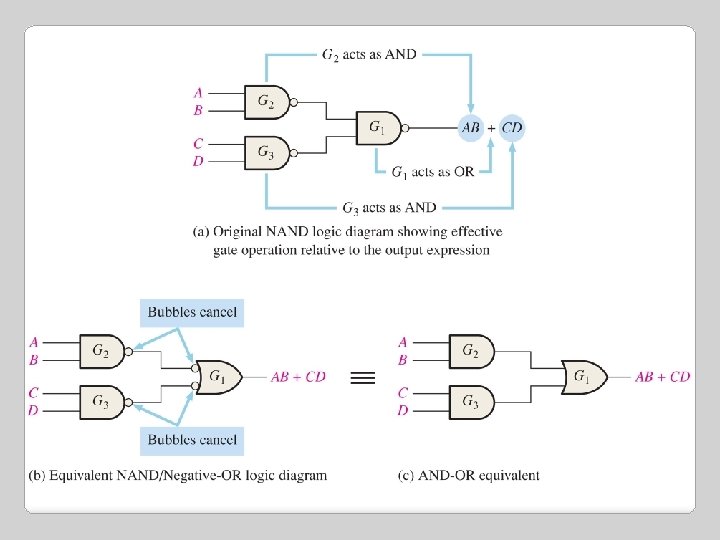
�Consider the NAND logic in Figure below. The output expression is developed in the following steps:
�The output expression, is in the form of two AND terms ORed together. This shows that gates G 2 and G 3 act as AND gates and that gate G 1 acts as an OR gate, ilustrated in figure (a) �This circuit redrawn in Figure (b) with NAND symbols for gates G 2 and G 3 and a negative OR symbol for gate G 1
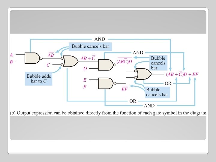
§NAND Logic Diagram Using Dual Symbols - All logic diagrams using NAND gates should be drawn with each gate represented by either a NAND symbol or the equivalent negative OR symbol to reflect the operation of the gate within the logic circuit. - The NAND symbol and negative OR symbol are called dual symbols. When drawing a NAND logic diagram, always use the gate symbols in such a way that every connection between a gate output and a gate input is either bubble to bubble or nonbubble to nonbubble. - A bubble output should not be connected to a nonbubble input or vice versa in a logic diagram.
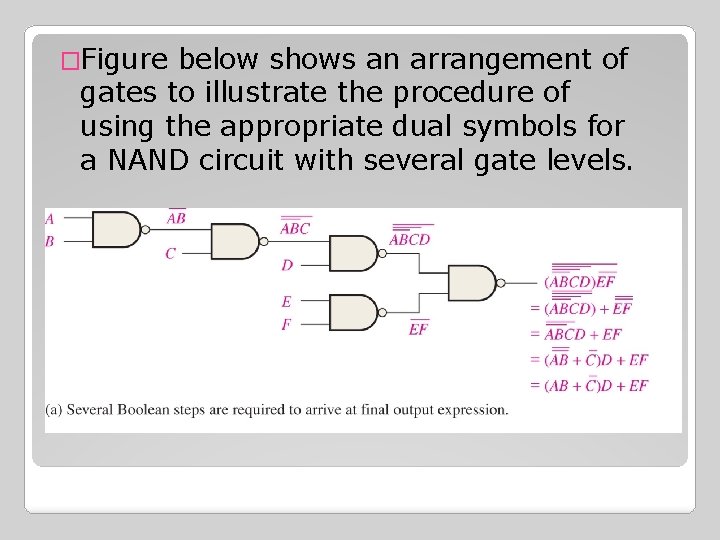
�Figure below shows an arrangement of gates to illustrate the procedure of using the appropriate dual symbols for a NAND circuit with several gate levels.
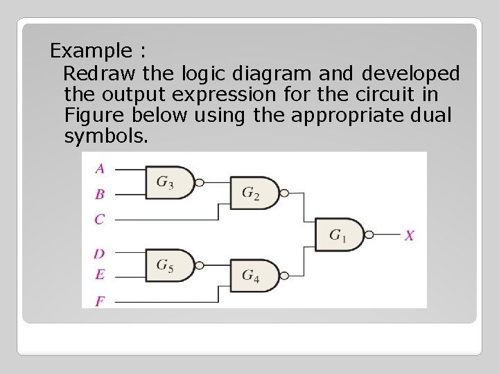
Example : Redraw the logic diagram and developed the output expression for the circuit in Figure below using the appropriate dual symbols.
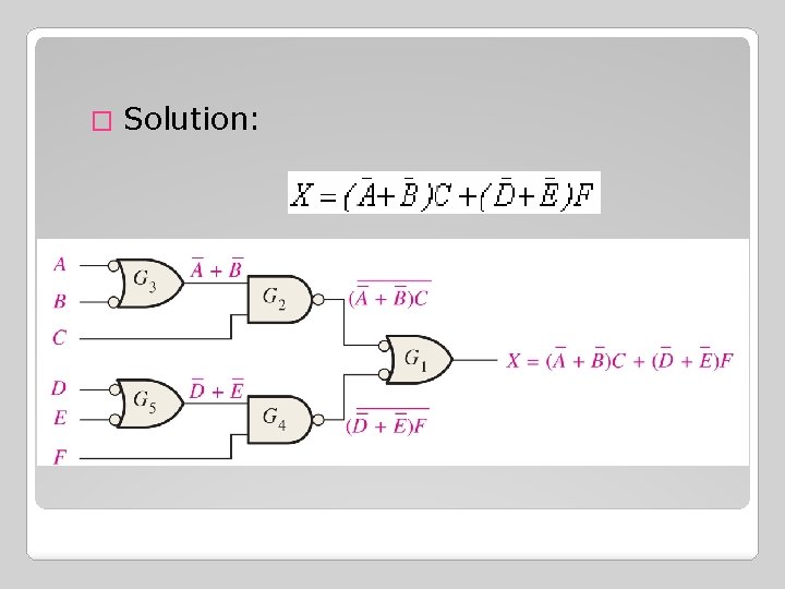
� Solution:
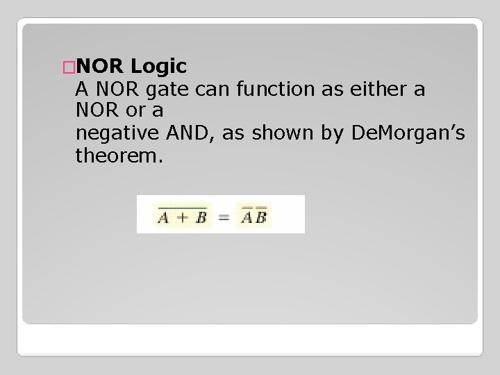
�NOR Logic A NOR gate can function as either a NOR or a negative AND, as shown by De. Morgan’s theorem.
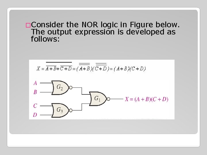
�Consider the NOR logic in Figure below. The output expression is developed as follows:
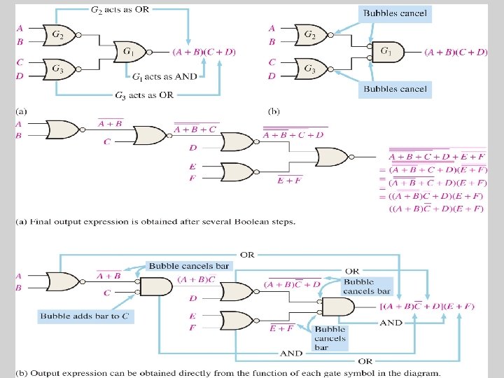
The output expression (A+B)(C+D) consists of two OR terms ANDed together. • This shows that gates G 2 and G 3 act as OR gates and gate G 1 acts as an AND gate. • This circuit is redrawn with a negative AND symbol for G 1 •
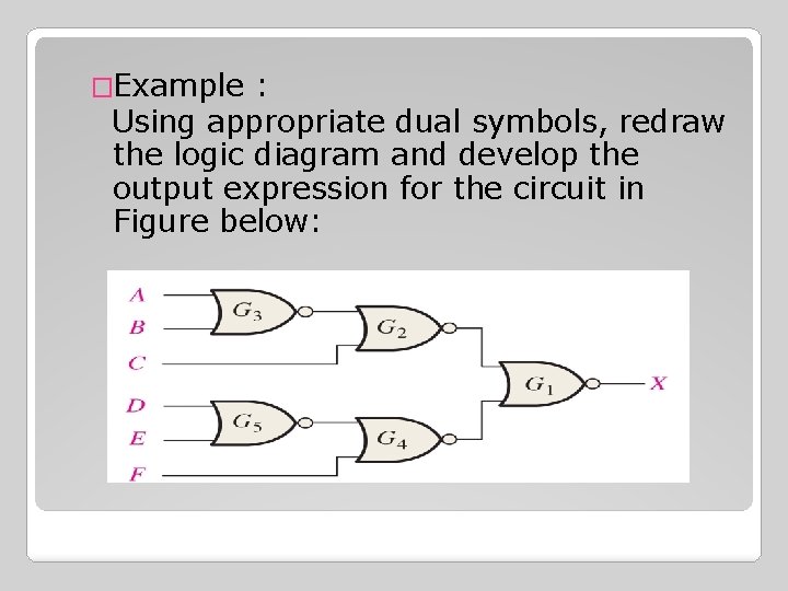
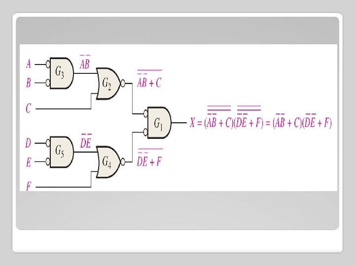
�Example : Using appropriate dual symbols, redraw the logic diagram and develop the output expression for the circuit in Figure below:
- Slides: 42