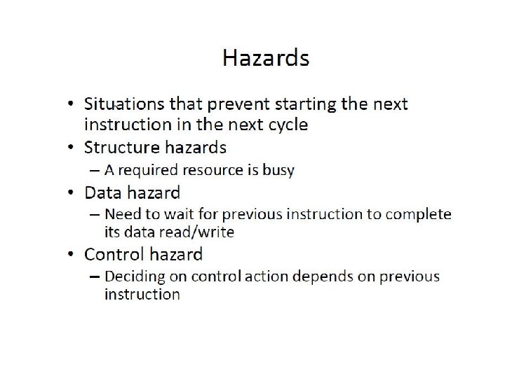
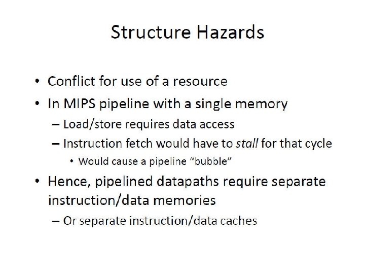
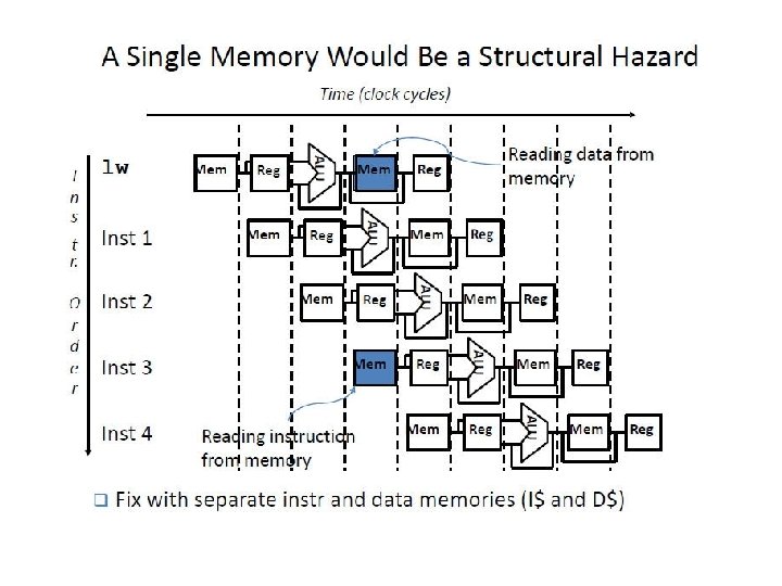
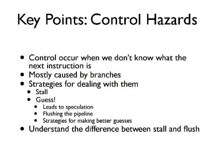
Processor Design Implementation Sequential vs Combinational Circuits Combinational

Processor Design & Implementation

Sequential vs Combinational Circuits • Combinational logic circuits • • output is a function of the present value of the inputs only. When inputs are changed, the information about the previous inputs is lost memoryless e. g. , multiplexors. • Sequential logic circuits • outputs are also dependent upon past inputs • has memory • basically combinational circuits with the additional properties of storage (to remember past inputs) and feedback • E. g. , latches, flip flops

RS Latches • An RS latch is a memory element with 2 inputs: - Reset (R) - Set (S) - 2 outputs: Q and Q Note: if inputs don’t change, outputs are held indefinitely.

RS Latches - Hold 0 1 0 0 0 1

RS Latches - Set 0 01 1 10 Reset 1 10 0 01

Clocks and Synchronous Circuits • Asynchronous operation : - the output state of RS latches changes occur directly in response to changes in the inputs. • Virtually all sequential circuits currently employ the notion of synchronous operation the output of a sequential circuit is constrained to change only at a time specified by a global enabling signal. This signal is generally known as the system clock

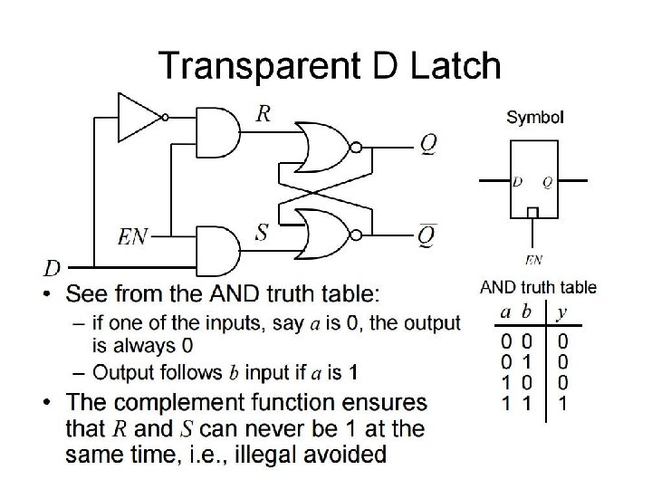
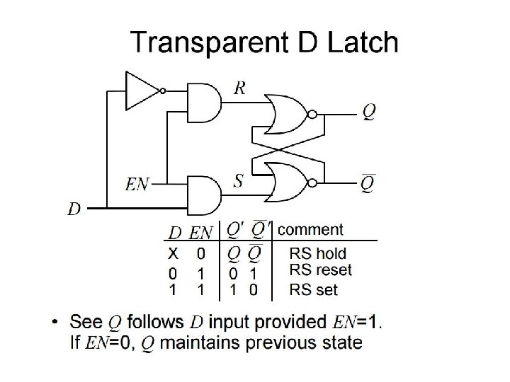
Transparent D Latches • modify the RS Latch such that its output state is only permitted to change when a valid enable signal (system clock) is present • Add a couple of AND gates in cascade with the R and S inputs that are controlled by an additional input known as the enable (EN) input

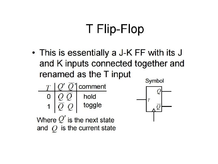
J-K Flip Flops

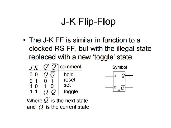
Race Around Condition only when J = K= clk = 1 Reset to 0 when input = 1 1, 0, 1 1 1, 0 = 1, 0, 1 = 0, 1, 0 When J = K= clk = 1: Output keeps toggling for the entire duration when clock is high How to solve this problem? Clk J K 0 1 1 x 0 1 Qn+1 (Qn+1)’ Qn Qn 0 1 ? (Qn)’ 1 (reset) 0 (set) ?

Race Around Condition only when J = K= clk = 1
 Flip Flops • Recall When J = K= clk")
Primary-Secondary (a. k. a. Master-Slave) Flip Flops • Recall When J = K= clk = 1: Output keeps toggling for the entire duration when clock is high. How to solve this problem? Easy to design sequential circuits if outputs change on: - rising (positive trending) - falling (negative trending) edges of a clock (i. e. , enable) signal Can be done by combining two transparent D latches in a Primary-Secondary configuration.

Primary-Secondary Flip Flops Primary FF 1 Secondary FF 0 0 0 1 1 All happening while clock is high 1

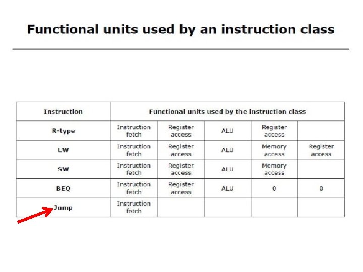
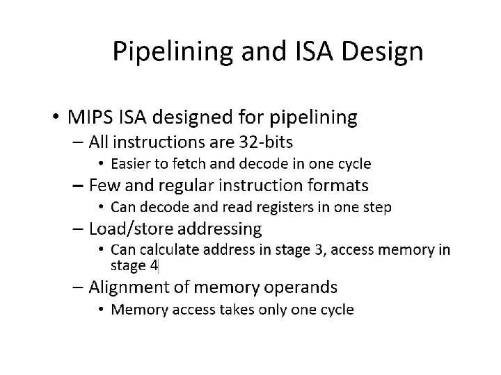
The Processor: Datapath & Control • Our implementation of the MIPS is simplified • memory-reference instructions: lw, sw • arithmetic-logical instructions: add, sub, and, or, slt • control flow instructions: beq, j • Generic implementation • use the program counter (PC) to supply the instruction address and fetch the instruction from memory (and update the PC) • decode the instruction (and read registers) • execute the instruction • All instructions (except j) use the ALU after reading the registers How? memory-reference? arithmetic? control flow? Fetch PC = PC+4 Exec Decode

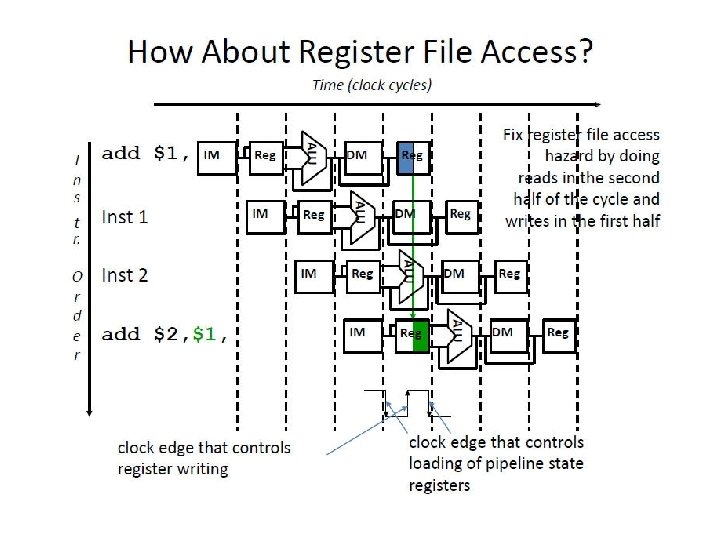
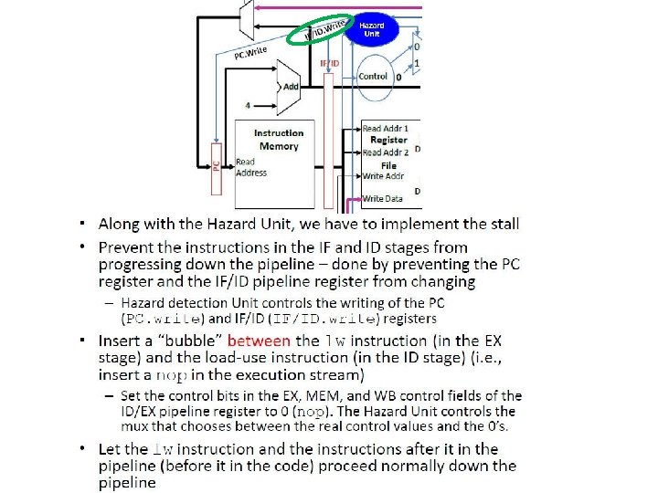
Aside: Clocking Methodologies • The clocking methodology defines when data in a state element is valid and stable relative to the clock • State elements - a memory element such as a register • Edge-triggered – all state changes occur on a clock edge • Typical execution • read contents of state elements -> send values through combinational logic -> write results to one or more state elements State element 1 Combinational logic State element 2 clock one clock cycle q Assumes state elements are written on every clock cycle; if not, need explicit write control signal l write occurs only when both the write control is asserted and the clock edge occurs

Fetch Phase • Fetching instructions involves • reading the instruction from the Instruction Memory • updating the PC value to be the address of the next (sequential) instruction Add clock 4 Fetch PC = PC+4 Exec l l Instruction Memory Decode PC Read Address Instruction PC is updated every clock cycle, so it does not need an explicit write control signal just a clock signal Reading from the Instruction Memory is a combinational activity, so it doesn’t need an explicit read control signal

Decoding Instructions • Decoding instructions involves • sending the fetched instruction’s opcode and function field bits to the control unit Control Unit Fetch PC = PC+4 Exec Decode Instruction Read Addr 1 Read Register Read Addr 2 Data 1 File Write Addr Read Write Data l Data 2 reading two values from the Register File - Register addresses (Read Addr 1 & Read Addr 2) are contained in the instruction
 31")
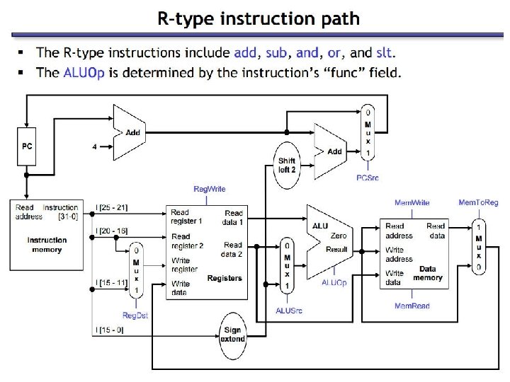
Executing R Format Operations • R format operations (add, sub, slt, and, or) 31 25 R-type: op rs 20 15 rt rd 10 5 0 shamt funct • perform operation (op and funct) on values in rs and rt • store the result back into the Register File (into location rd) Reg. Write ALU control (3 bit code) Read Addr 1 Fetch PC = PC+4 Instruction Read Register Data 1 Read Addr 2 File Write Addr Exec Decode Write Data ALU overflow zero Read Data 2 Register File is not written every cycle (e. g. , sw) need an explicit write control signal (Reg. Write) for the it. l

Executing Load and Store Operations • Load and store operations involves • compute memory address by adding the base register (read from the Register File during decode) to the 16 -bit signed-extended offset field in the instruction, e. g. , sw $s 3 4($t 5) • store value (read from the Register File during decode) written to the Data Memory, • load value, read from the Data Memory, written to the Register File Reg. Write Instruction Read Addr 1 Read Register Read Addr 2 Data 1 File Write Addr Read Write Data 16 ALU control $t 5 4 Data 2 Sign Extend Mem. Write overflow zero Address ALU Data Memory Read Data Write Data Mem. Read 32

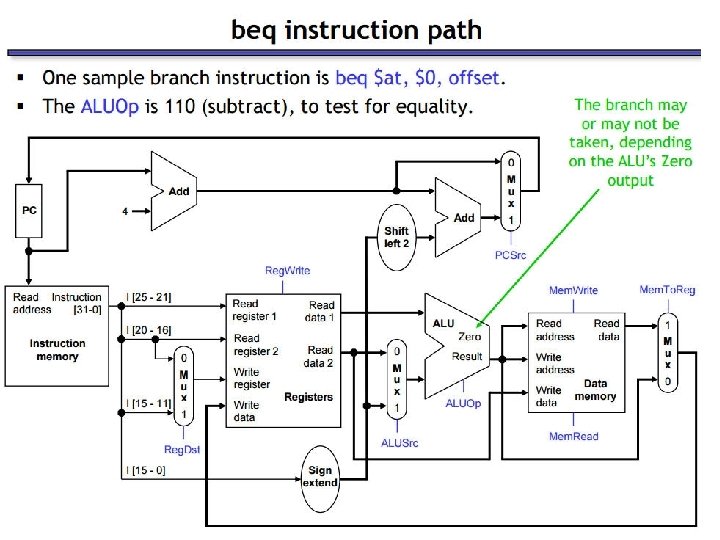
Branch Addressing Branch instructions specify - opcode, two registers, target address Most branch targets are near branch - Forward or backward n op rs rt constant or address 6 bits 5 bits 16 bits PC-relative addressing n Target address = PC + offset × 4 n PC already incremented by 4 by this time

Executing Branch Operations • Branch operations involves • compare the operands read from the Register File during decode for equality (zero ALU output) • compute the branch target address by adding the updated PC to the 16 -bit signed-extended offset field in the instr Why << 2? Add 4 Add Shift left 2 Branch target address ALU control (3 bit code) PC Instruction Read Addr 1 Register Read Addr 2 Data 1 File Write Addr Read Write Data 16 Data 2 Sign Extend 32 zero (to branch control logic) ALU
 targets could be anywhere in text segment �Encode")
Jump Addressing �Jump (j and jal) targets could be anywhere in text segment �Encode full address in instruction n op address 6 bits 26 bits (Pseudo)Direct jump addressing n Target address = PC 31… 28 : (address × 4) Chapter 2 — Instructions: Language of the Computer — 30

Executing Jump Operations • Jump operation involves • replace the lower 28 bits of the PC with the lower 26 bits of the fetched instruction shifted left by 2 bits • Target address = PC 31… 28 : (address × 4) Add 4 4 Instruction Memory PC Read Address Instruction Shift left 2 26 Jump address 28

Creating a Single Datapath from the Parts • Assemble the datapath segments and add control lines and multiplexors as needed • Single cycle design – fetch, decode and execute each instructions in one clock cycle • no datapath resource can be used more than once per instruction, so some must be duplicated (e. g. , separate Instruction Memory and Data Memory, several adders) • multiplexors needed at the input of shared elements with control lines to do the selection • write signals to control writing to the Register File and Data Memory • Cycle time is determined by length of the longest path
 • Here is")
Multiplexors 2 Input 1 Bit Selector Device (2 x 1 MUX) • Here is a truth table definition of a “function” we wish to implement: S A B output 0 0 0 1 0 1 1 0 0 0 1 1 1 1 0 0 1 1 • When S = 0, A is “selected” for output • When S = 1, B is “selected” for output
 • What is the Boolean expression for")
• 2 x 1 MUX (Multiplexor) • What is the Boolean expression for a 2 x 1 MUX? Output = S • B + S • A S A B output 0 0 0 1 0 1 1 0 0 0 1 1 1 1 0 0 1 1 • How do you implement this using gates? A B output S (control signal)
 and ALUs - To select a source input for ALU From Register")
Multiplexors (MUX) and ALUs - To select a source input for ALU From Register From instruction field M U X Control signal A L U

Fetch, R, and Memory Access Portions Reg. Write Add ALUSrc ALU control 4 Instruction Memory PC Read Address Instruction - multiplexor (mux) Memto. Reg ovf zero Read Addr 1 Register Read Addr 2 Data 1 File Write Addr Read Data 2 Write Data Sign 16 Extend Mem. Write Address ALU Data Memory Read Data Write Data Mem. Read 32 - ALU (adder)

Adding the Control • Selecting the operations to perform (ALU, Register File and Memory read/write) • Controlling the flow of data (multiplexor inputs) 31 R-type: op q Observations l l op field always in bits 31 -26 31 I-Type: op 31 25 rs 20 15 rt rd 20 rt 10 5 0 shamt funct 15 0 address offset 25 addr of registers J-type: op target address to be read are always specified by the rs field (bits 25 -21) and rt field (bits 20 -16); for lw and sw rs is the base register l addr. of register to be written is in one of two places – in rt (bits 20 -16) for lw; in rd (bits 15 -11) for R-type instructions l offset for beq, lw, and sw always in bits 15 -0 0

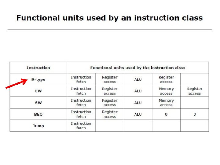
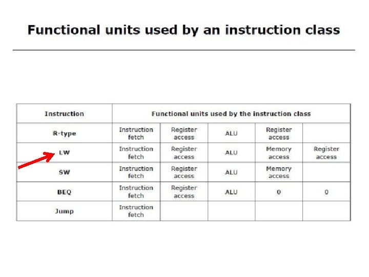
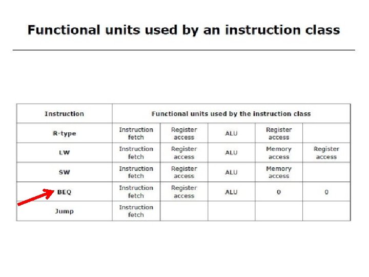
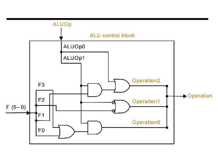
Control The control unit is responsible for setting all the control signals so that each instruction is executed properly. — The control unit’s input is the 32 -bit instruction word. — The outputs are values for the control signals in the datapath. Most of the signals can be generated from the instruction opcode alone, and not the entire 32 -bit word. To illustrate the relevant control signals, we will show the route that is taken through the datapath by R-type, lw, sw and beq instructions.
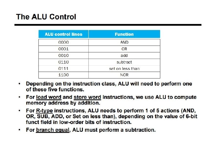
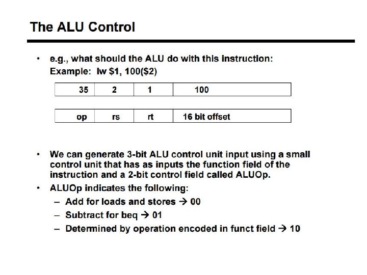
![ALU Control Unit 0 Add ALUOp Reg. Dst PC Read Address Instr[31 -0] Mem.](http://slidetodoc.com/presentation_image_h2/9b5bc3fbc0a35f041a7f2cc45d0b331f/image-41.jpg "ALU Control Unit 0 Add ALUOp Reg. Dst PC Read Address Instr[31 -0] Mem.")
ALU Control Unit 0 Add ALUOp Reg. Dst PC Read Address Instr[31 -0] Mem. Read Memto. Reg Mem. Write ALUSrc Reg. Write ovf Instr[25 -21] Read Addr 1 Register Read Instr[20 -16] Read Addr 2 Data 1 File 0 Write Addr Read 1 Instr[15 -11] Instr[15 -0] 1 PCSrc Branch Instr[31 -26] Control Unit Instruction Memory Add Shift left 2 4 Write Data zero 0 ALU Data 2 1 Sign 16 Extend 32 4 ALU control Instr[5 -0] 2 Address Data Memory Read Data 1 Write Data 0

Can ignore use XX don’t cares


4
![Bit I/O for ALU Control Unit 0 Add ALUOp Instr[31 -26] Control Unit PC](http://slidetodoc.com/presentation_image_h2/9b5bc3fbc0a35f041a7f2cc45d0b331f/image-46.jpg "Bit I/O for ALU Control Unit 0 Add ALUOp Instr[31 -26] Control Unit PC")
Bit I/O for ALU Control Unit 0 Add ALUOp Instr[31 -26] Control Unit PC Read Address Instr[31 -0] Mem. Read Memto. Reg Mem. Write ALUSrc Reg. Write ovf Instr[25 -21] Read Addr 1 Register Read Instr[20 -16] Read Addr 2 Data 1 File 0 Write Addr Read 1 Instr[15 -11] Instr[15 -0] 1 PCSrc Branch Reg. Dst Instruction Memory Add Shift left 2 4 Write Data zero 0 ALU Data 2 1 Sign 16 Extend 32 4 ALU control Instr[5 -0] 2 Address Data Memory Read Data 1 Write Data 0

R-type Instruction 31 R-type: op 31 25 rs 25 20 15 rt rd 20 15 10 5 0 shamt funct 0
![R-type Dataflow 0 Add ALUOp Reg. Dst PC Read Address Instr[31 -0] 1 PCSrc](http://slidetodoc.com/presentation_image_h2/9b5bc3fbc0a35f041a7f2cc45d0b331f/image-49.jpg "R-type Dataflow 0 Add ALUOp Reg. Dst PC Read Address Instr[31 -0] 1 PCSrc")
R-type Dataflow 0 Add ALUOp Reg. Dst PC Read Address Instr[31 -0] 1 PCSrc Branch Instr[31 -26] Control Unit Instruction Memory Add Shift left 2 4 Mem. Read Memto. Reg ALUSrc Mem. Write Reg. Write ovf Instr[25 -21][rs] Read Addr 1 Instr[20 -16][rt] Register Read Addr 2 Data 1 File 0 Write Addr Read 1 Instr[15 -11][rd] Write Data Instr[15 -0] zero 0 ALU Data 2 1 Sign 16 Extend 32 Instr[5 -0] ALUOp ALU control Address Data Memory Read Data 1 Write Data 0

R type - Control Lines 0 0 1

0010

Load Word Instruction Data/Control Flow 0 Add ALUOp Reg. Dst Mem. Read Memto. Reg Mem. Write ALUSrc Reg. Write ovf Instr[25 -21] PC Read Address Instr[31 -0] Read Addr 1 Register Read Instr[25 -21] Read Addr 2 Data 1 File 0 Write Addr Read 1 Instr[15 -11] Instr[15 -0] lw $s 1, 32($t 0) 1 PCSrc Branch Instr[31 -26] Control Unit Instruction Memory Add Shift left 2 4 Write Data zero 0 ALU Data 2 1 Sign 16 Extend 32 Instr[5 -0] ALU control Address Data Memory Read Data 1 Write Data 0

Load Word Instruction Data/Control Flow 0 Add Shift left 2 4 1 PCSrc Branch Instr[31 -26] Control Unit Reg. Dst Instruction Memory PC Read Address Instr[31 -0] ALUSrc Instr[25 -21] Read Addr 1 $t 0 Register Read Instr[20 -16] Read Addr 2 Data 1 File 0 $s 1 Write Addr Read Instr[15 -11] Instr[15 -0] Mem. Write ovf 1 lw $s 1, 32($t 0) Memto. Reg. Write Data 2 Sign 16 Extend 32 32 zero 0 ALU Address Data Memory Read Data 1 Write Data 0 1 ALU control Instr[5 -0] ALUOp Mem. Read

lw - Control Lines 0 0 1 1

$sp 16 / 32 $a 0

Branching 31 I-Type: op 25 rs 20 rt 15 0 address offset
![Branch Instruction Data/Control Flow 0 Add ALUOp Reg. Dst PC Read Address Instr[31 -0]](http://slidetodoc.com/presentation_image_h2/9b5bc3fbc0a35f041a7f2cc45d0b331f/image-58.jpg "Branch Instruction Data/Control Flow 0 Add ALUOp Reg. Dst PC Read Address Instr[31 -0]")
Branch Instruction Data/Control Flow 0 Add ALUOp Reg. Dst PC Read Address Instr[31 -0] ALUSrc Reg. Write ovf 1 beq $t 0, $t 1, addr Mem. Read Memto. Reg Mem. Write Instr[25 -21] Read Addr 1 Register Read Instr[20 -16] Read Addr 2 Data 1 File 0 Write Addr Read Instr[15 -11] Instr[15 -0] 1 PCSrc Branch Instr[31 -26] Control Unit Instruction Memory Add Shift left 2 4 Write Data zero 0 ALU Data 2 1 Sign 16 Extend 32 Instr[5 -0] ALU control Address Data Memory Read Data 1 Write Data 0
![Branch Instruction Data/Control Flow 0 Add ALUOp Reg. Dst PC Read Address Instr[31 -0]](http://slidetodoc.com/presentation_image_h2/9b5bc3fbc0a35f041a7f2cc45d0b331f/image-59.jpg "Branch Instruction Data/Control Flow 0 Add ALUOp Reg. Dst PC Read Address Instr[31 -0]")
Branch Instruction Data/Control Flow 0 Add ALUOp Reg. Dst PC Read Address Instr[31 -0] ALUSrc Reg. Write ovf 1 beq $t 0, $t 1, addr Mem. Read Memto. Reg Mem. Write Instr[25 -21] Read Addr 1 $t 0 Register Read Instr[20 -16] Read Addr 2 Data 1 $t 1 File 0 Write Addr Read Instr[15 -11] Instr[15 -0] 1 PCSrc Branch Instr[31 -26] Control Unit Instruction Memory Add Shift left 2 4 Write Data zero 0 ALU Data 2 1 Sign 16 Extend 32 Instr[5 -0] ALU control Address Data Memory Read Data 1 Write Data 0

Main Control Lines 1 0

31 J-type: op 25 0 target address
 A<<2 to make it 28 bits Target addr")
if addr = A (26 bits) A<<2 to make it 28 bits Target addr = PC[31 -28]: A 00 Jump Instr[25 -0] Shift 26 left 2 25 -0] 28 1 32 PC: 4[31 -28] 0 0 Add j ALUOp addr Branch Instr[31 -26] Control Unit Reg. Dst Instruction Memory PC Read Address Instr[31 -0] Jump PCSrc ALUSrc Reg. Write ovf 1 Instr[15 -0] 1 Mem. Read Memto. Reg Mem. Write Instr[25 -21] Read Addr 1 Register Read Instr[20 -16] Read Addr 2 Data 1 File 0 Write Addr Read Instr[15 -11] Add Shift left 2 4 Write Data zero 0 ALU Data 2 1 Sign 16 Extend 32 Instr[5 -0] ALU control Address Data Memory Read Data 1 Write Data 0

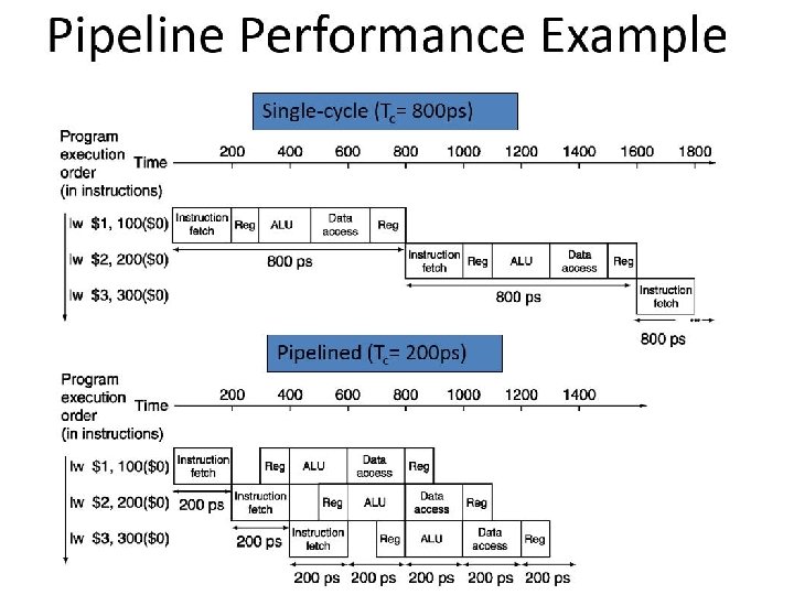
Single Cycle Disadvantages & Advantages • Uses the clock cycle inefficiently – the clock cycle must be timed to accommodate the slowest instruction • especially problematic for more complex instructions like floating point multiply Cycle 1 Cycle 2 Clk lw 800 ps sw Waste 700 ps • May be wasteful of area since some functional units (e. g. , adders) must be duplicated since they can not be shared during a clock cycle but is simple and easy to understand

Instruction Critical Paths What is the clock cycle time assuming negligible delays for muxes, control unit, sign extend, PC access, shift left 2, wires, setup and hold times except: q l Instruction and Data Memory access (200 ps) l ALU and adders (200 ps) l Register File access (reads or writes) (100 ps)

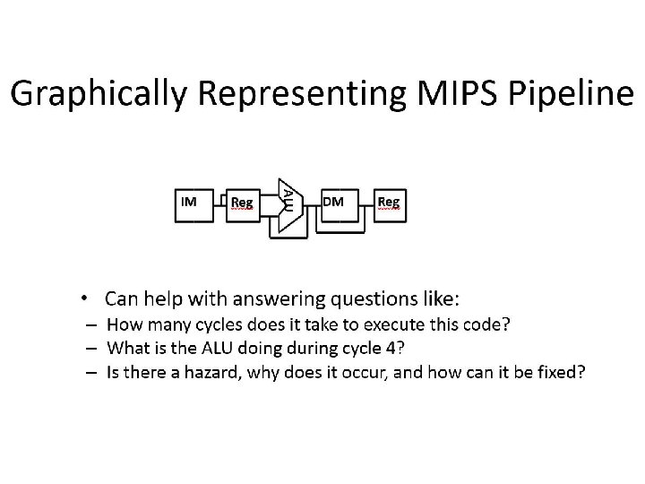
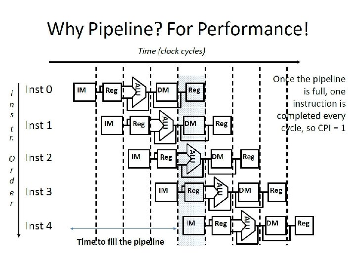
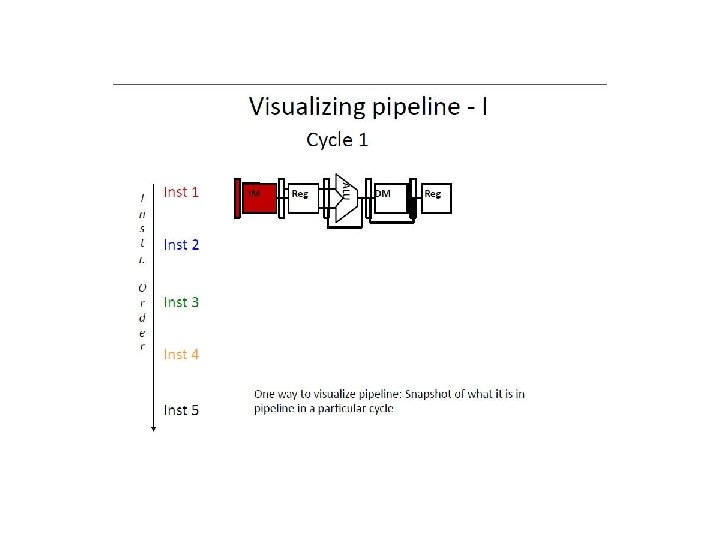
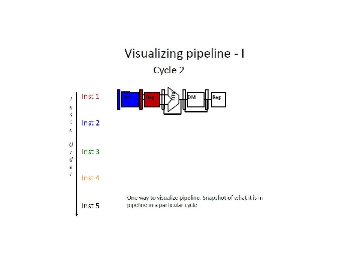
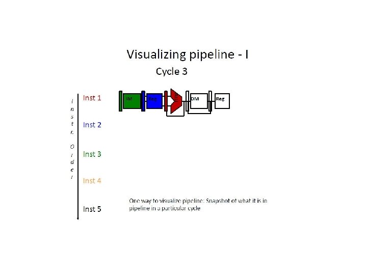
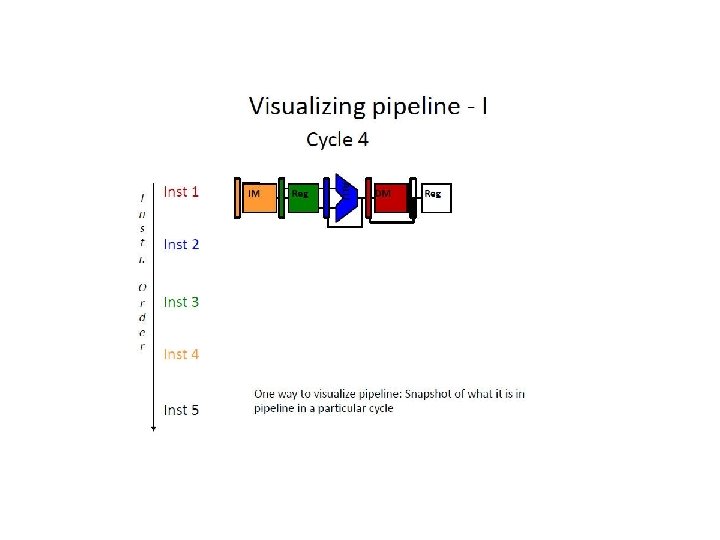
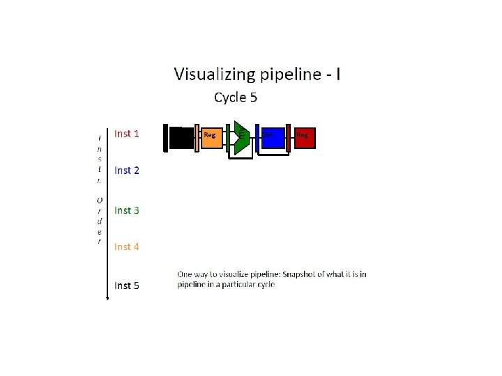
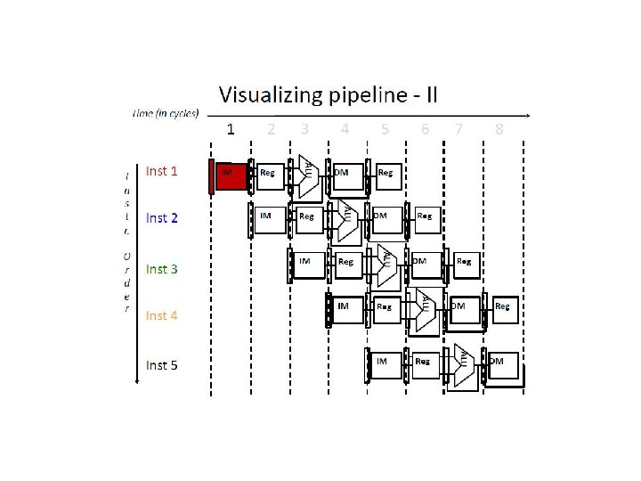
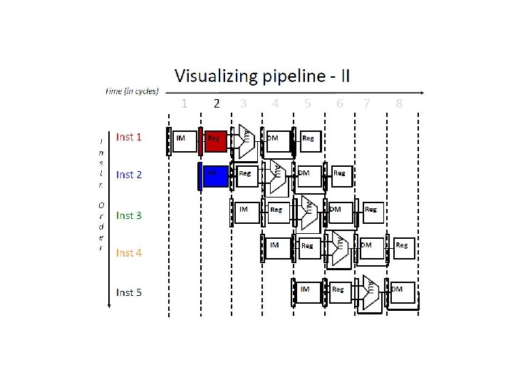
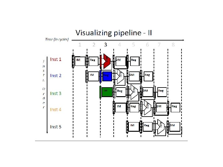
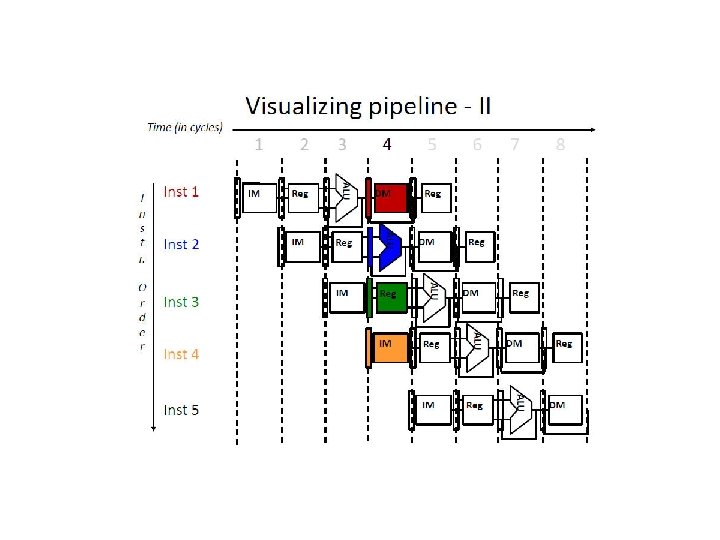
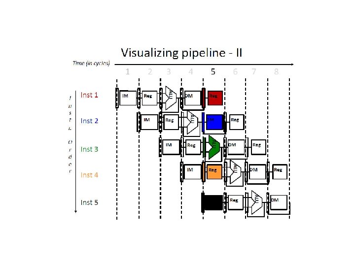
How Can We Make It Faster? • Start fetching and executing the next instruction before the current one has completed • Pipelining – (all? ) modern processors are pipelined for performance • The performance metric: CPU time = Cycles/Instr * Clk Cycle * Total # Instr • Under ideal conditions and with a large number of instructions, the speedup from pipelining is approximately equal to the number of pipe stages • A five stage pipeline is nearly five times faster because the clk cycle is nearly five times faster q Fetch (and execute) more than one instruction at a time

Pipelining Analogy Pipelined laundry: overlapping execution Parallelism improves performance Four loads: Sequential = 8 hrs Pipelined = 3. 5 hrs Speedup = 8/3. 5 = 2. 3

Pipelining Speedup five-stage pipeline should offer nearly a fivefold improvement over the nonpipelined time, or a 160 ps clock cycle. Pipelining has some issues actual speedup < # stages.
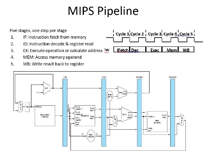

f = Fetch r = Register read a = ALU op d = Data access w = Writeback
 and write PC (on")
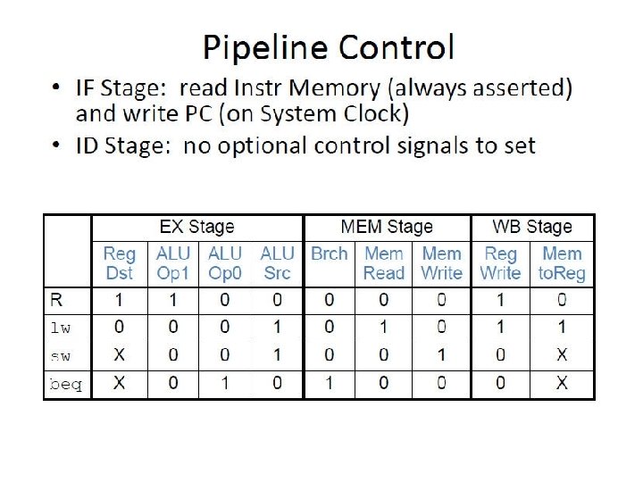
Pipeline Control • IF Stage: read Instr Memory (always asserted) and write PC (on System Clock) • ID Stage: no optional control signals to set EX Stage R lw Reg Dst 1 MEM Stage WB Stage ALU ALU Brch Mem Reg Mem Op 1 Op 0 Src Read Write to. Reg 1 0 0 0 1 0 1 1 sw X 0 0 1 0 X beq X 0 1 0 0 0 X

W R
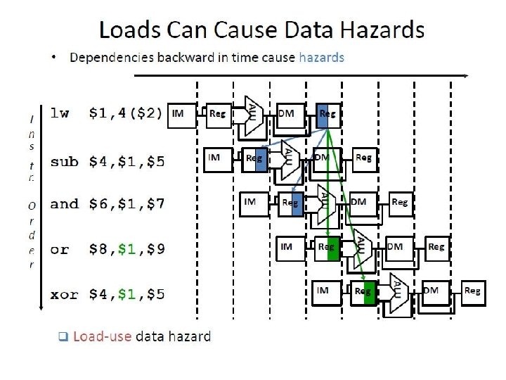
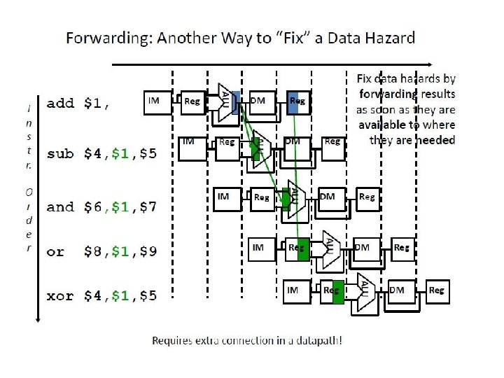

Output from ALU of 1 st instruction has to be forwarded to Instr#2 and #3 Since only one output (from ALU) can be forwarded, it is sent to Instr#2 Instr#3’s ALU must wait till the next stage to get output of 1 st Instr’s ALU

IF ? ? ID EX MEM WB

Why?

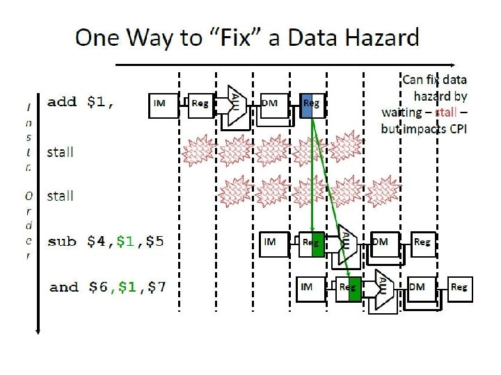
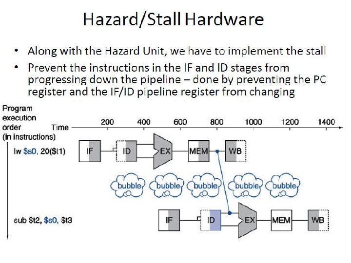
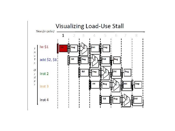
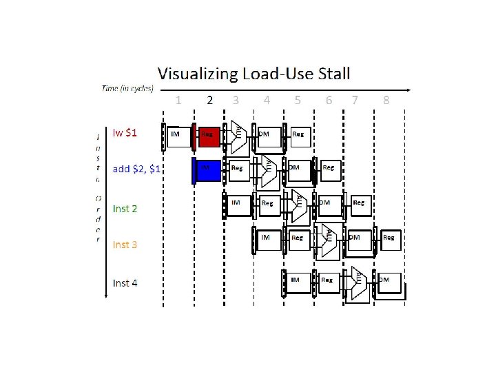
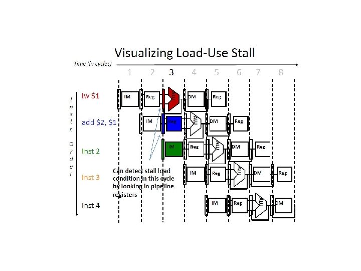
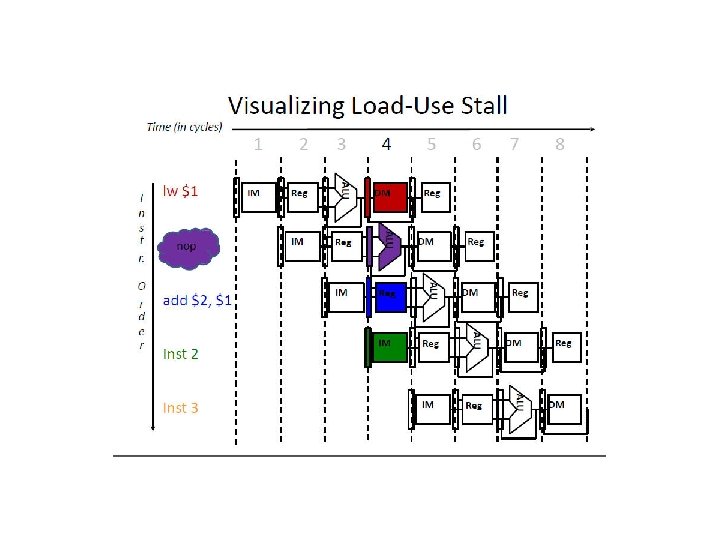
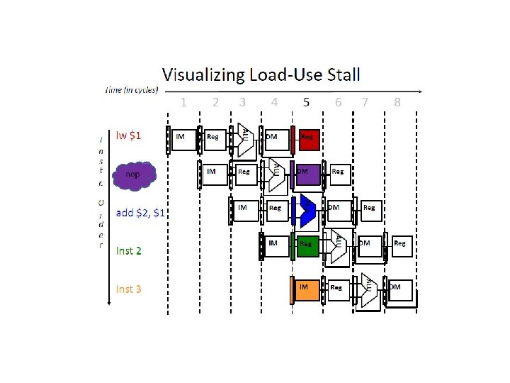
Why 13 cycles? Cycles 1 2 3 4 5 6 7 8 9 10 11 12 13 Instr 1 2 (stall) 3 4 5 (stall) 6 7

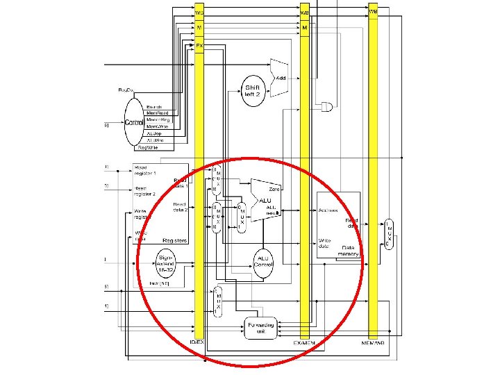
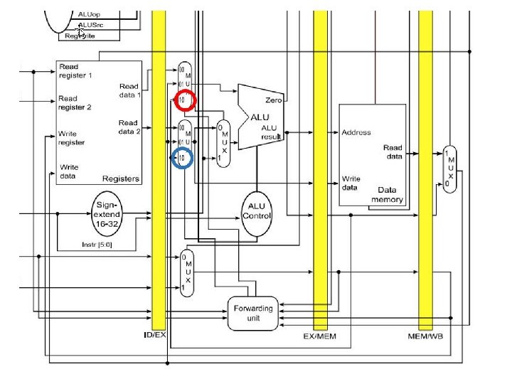
Forwarding Unit
")
Forwarding Unit Inputs For ALU result For WB (from Memory)

Forwarding Example $t 1 $t 0 $t 1

$t 1 $t 0 $t 1

Add $t 0, add $t 0, or $t 1, Х Х sub _ , _, _ $t 0, $t 0 (if one instr away, can forward at MEM
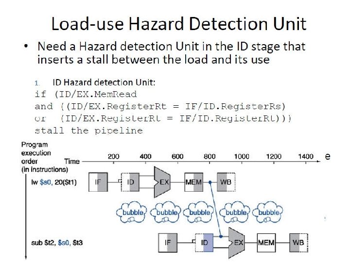
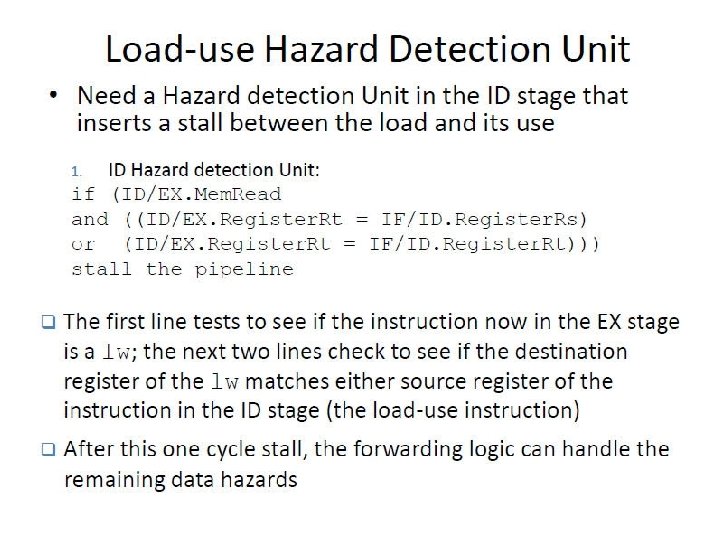

Hazard Unit
- Slides: 128