Sequential Circuit Counter INTRODUCTION A counter a group


- Slides: 65

Sequential Circuit - Counter -

INTRODUCTION • A counter – a group of flip-flops connected together to perform counting operations. • The number of flip-flops used and the way in which they are connected determine the number of states (modulus). • Two broad categories according to the way they are clocked: • Asynchronous counter • Synchronous counter

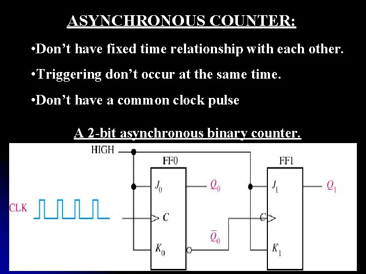
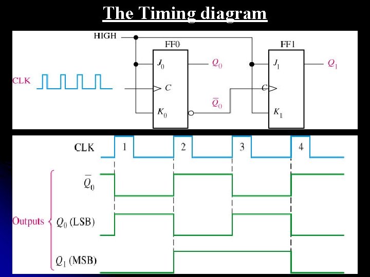
ASYNCHRONOUS COUNTER: • Don’t have fixed time relationship with each other. • Triggering don’t occur at the same time. • Don’t have a common clock pulse A 2 -bit asynchronous binary counter.

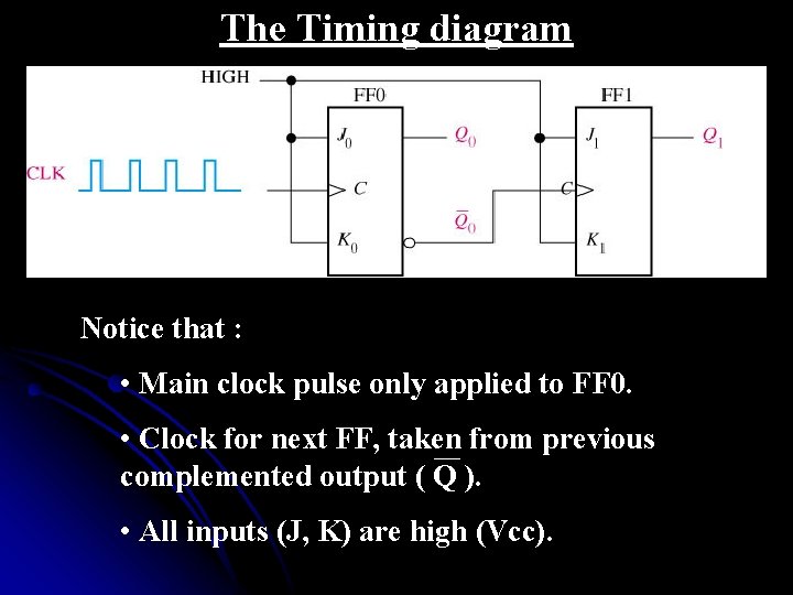
The Timing diagram Notice that : • Main clock pulse only applied to FF 0. • Clock for next FF, taken from previous complemented output ( Q ). • All inputs (J, K) are high (Vcc).

The Timing diagram

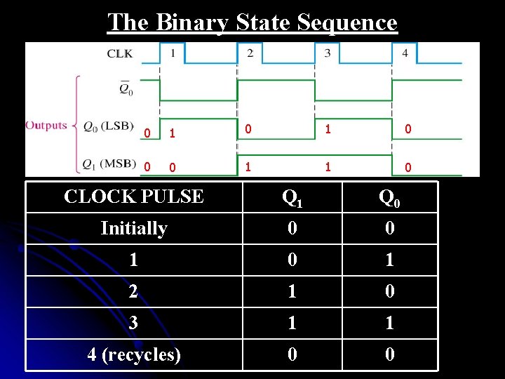
The Binary State Sequence 0 1 0 0 0 1 1 0 CLOCK PULSE Q 1 Q 0 Initially 0 0 1 2 1 0 3 1 1 4 (recycles) 0 0

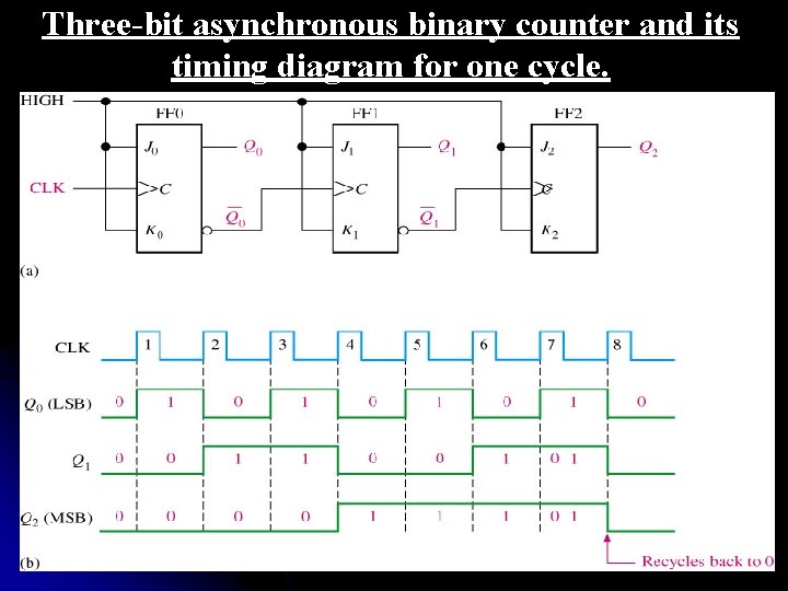
Three-bit asynchronous binary counter and its timing diagram for one cycle.

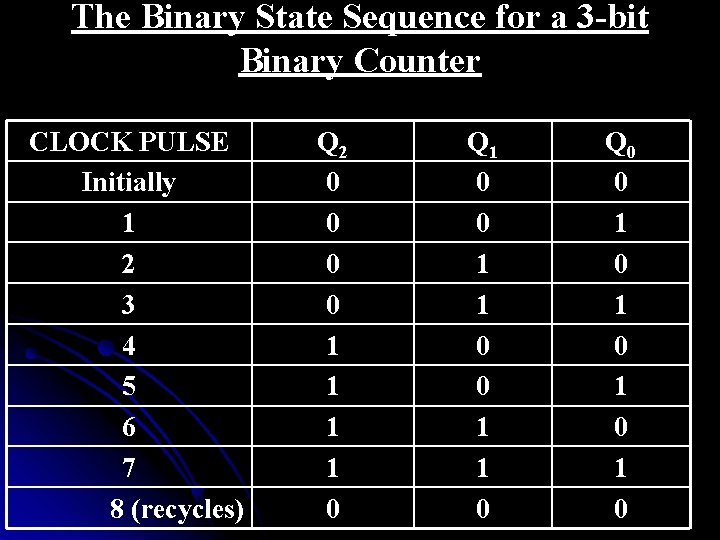
The Binary State Sequence for a 3 -bit Binary Counter CLOCK PULSE Initially 1 2 3 4 5 6 7 8 (recycles) Q 2 0 0 1 1 0 Q 1 0 0 1 1 0 Q 0 0 1 0 1 0

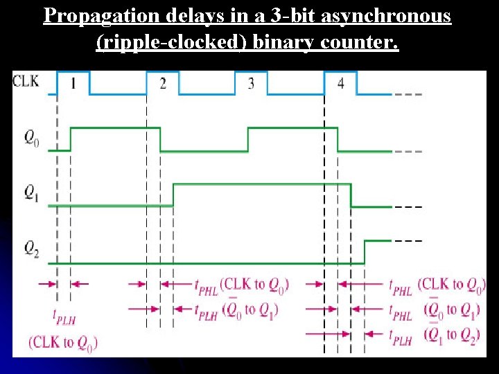
Propagation delays in a 3 -bit asynchronous (ripple-clocked) binary counter.

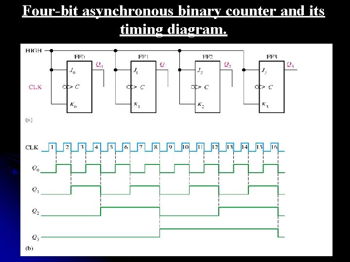
Four-bit asynchronous binary counter and its timing diagram.

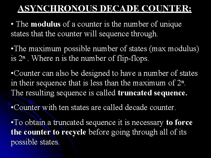
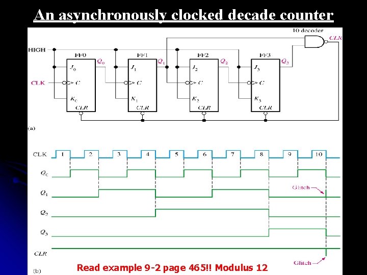
ASYNCHRONOUS DECADE COUNTER: • The modulus of a counter is the number of unique states that the counter will sequence through. • The maximum possible number of states (max modulus) is 2 n. Where n is the number of flip-flops. • Counter can also be designed to have a number of states in their sequence that is less than the maximum of 2 n. The resulting sequence is called truncated sequence. • Counter with ten states are called decade counter. • To obtain a truncated sequence it is necessary to force the counter to recycle before going through all of its possible states.

An asynchronously clocked decade counter Read example 9 -2 page 465!! Modulus 12

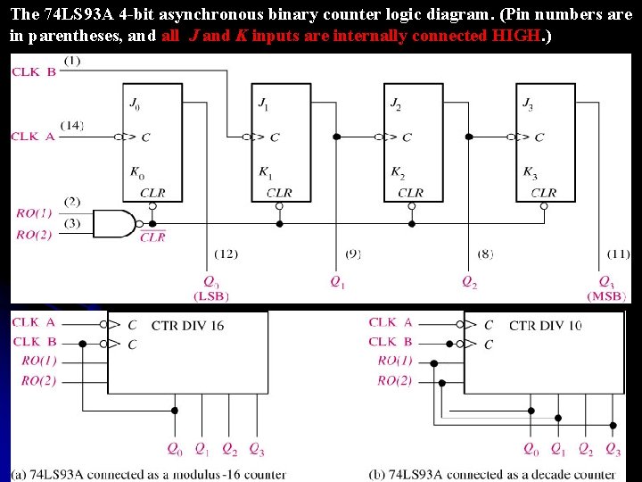
The 74 LS 93 A 4 -bit asynchronous binary counter logic diagram. (Pin numbers are in parentheses, and all J and K inputs are internally connected HIGH. )

Comprehending Engineers… To the optimist, the glass is half full. l To the pessimist, the glass is half empty. l To the engineers. . ? l The glass is twice as big as it needs to be.

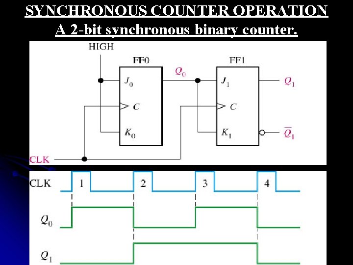
SYNCHRONOUS COUNTER OPERATION A 2 -bit synchronous binary counter.

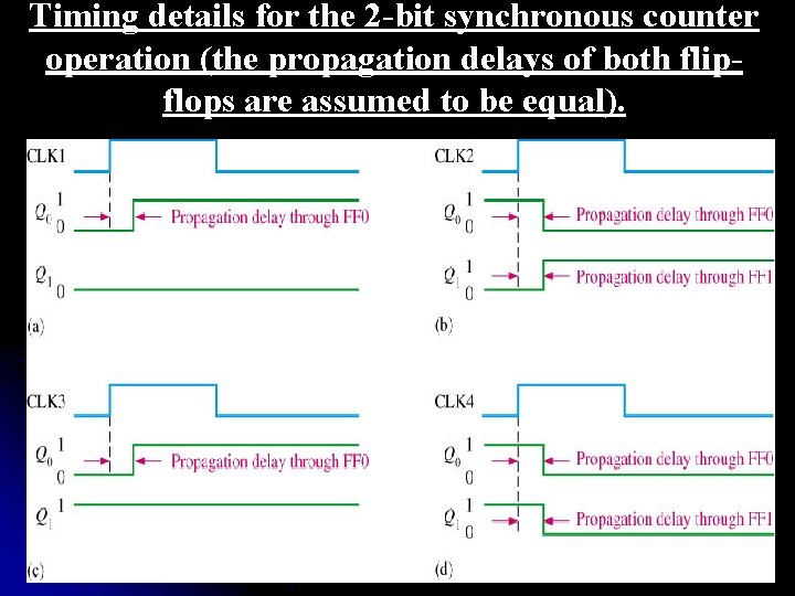
Timing details for the 2 -bit synchronous counter operation (the propagation delays of both flipflops are assumed to be equal).

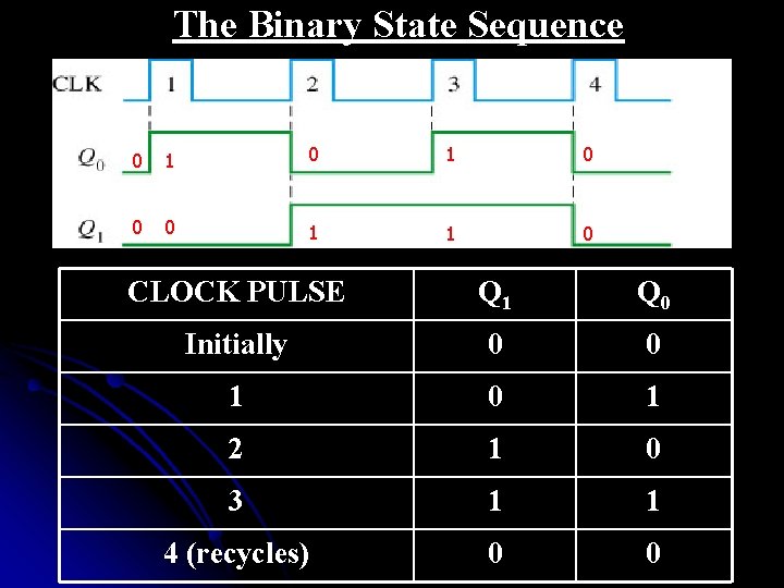
The Binary State Sequence 0 1 0 0 0 1 1 0 CLOCK PULSE Q 1 Q 0 Initially 0 0 1 2 1 0 3 1 1 4 (recycles) 0 0

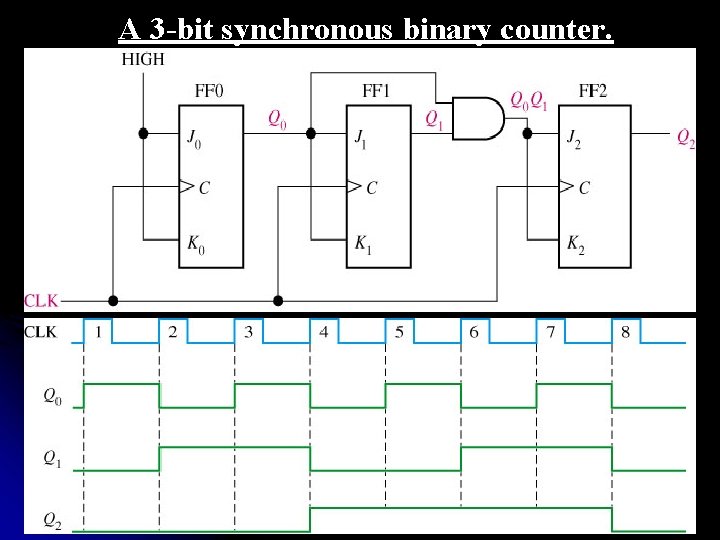
A 3 -bit synchronous binary counter.

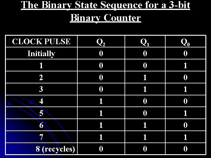
The Binary State Sequence for a 3 -bit Binary Counter CLOCK PULSE Initially 1 2 3 4 5 6 7 8 (recycles) Q 2 0 0 1 1 0 Q 1 0 0 1 1 0 Q 0 0 1 0 1 0

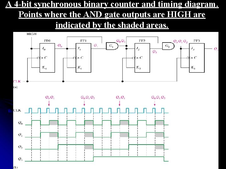
A 4 -bit synchronous binary counter and timing diagram. Points where the AND gate outputs are HIGH are indicated by the shaded areas.

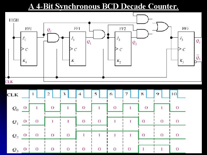
A 4 -Bit Synchronous BCD Decade Counter.

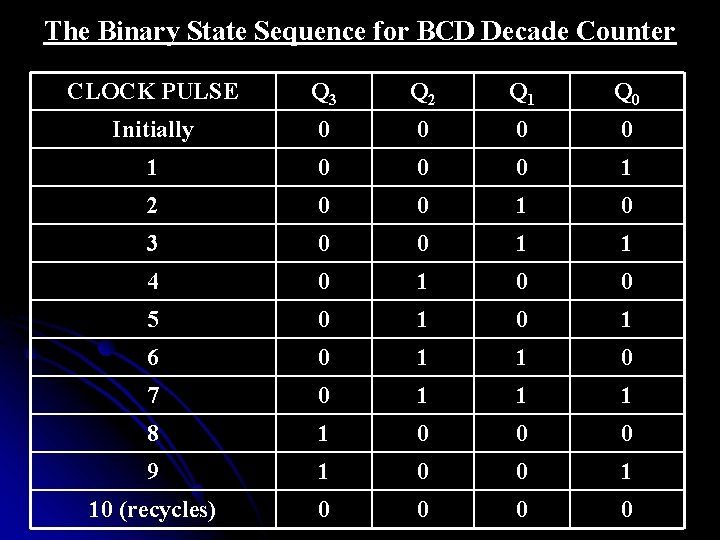
The Binary State Sequence for BCD Decade Counter CLOCK PULSE Q 3 Q 2 Q 1 Q 0 Initially 0 0 1 0 0 0 1 2 0 0 1 0 3 0 0 1 1 4 0 1 0 0 5 0 1 6 0 1 1 0 7 0 1 1 1 8 1 0 0 0 9 1 0 0 1 10 (recycles) 0 0

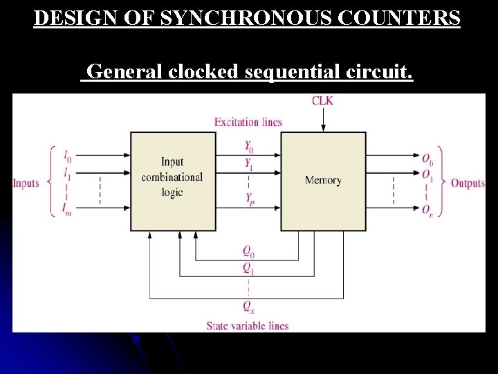
DESIGN OF SYNCHRONOUS COUNTERS General clocked sequential circuit.

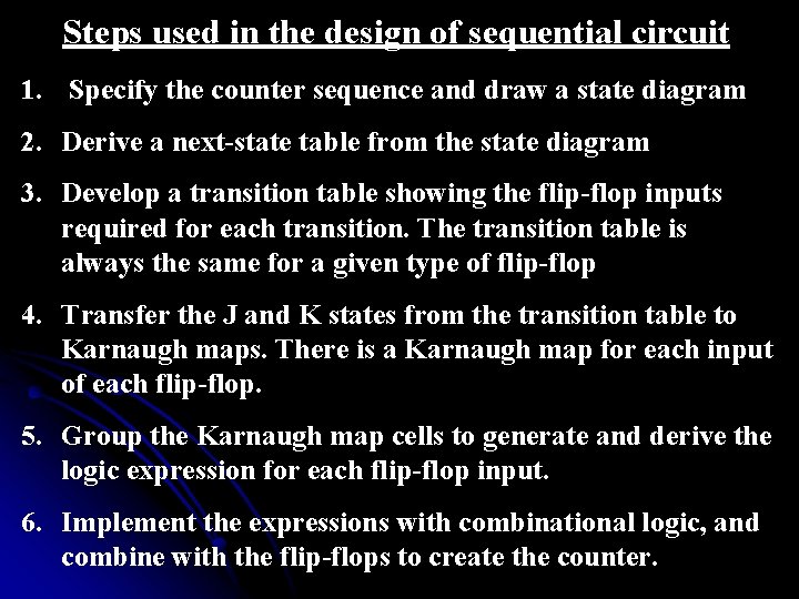
Steps used in the design of sequential circuit 1. Specify the counter sequence and draw a state diagram 2. Derive a next-state table from the state diagram 3. Develop a transition table showing the flip-flop inputs required for each transition. The transition table is always the same for a given type of flip-flop 4. Transfer the J and K states from the transition table to Karnaugh maps. There is a Karnaugh map for each input of each flip-flop. 5. Group the Karnaugh map cells to generate and derive the logic expression for each flip-flop input. 6. Implement the expressions with combinational logic, and combine with the flip-flops to create the counter.

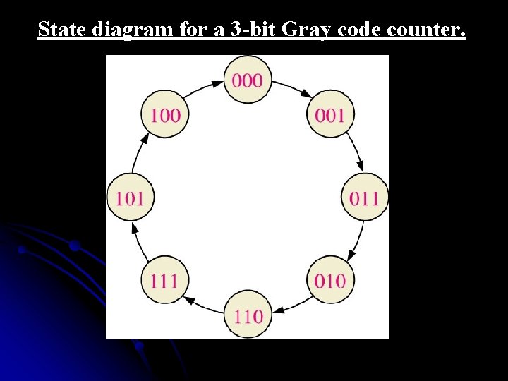
State diagram for a 3 -bit Gray code counter.

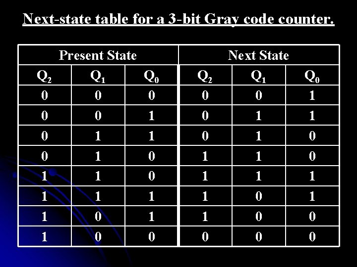
Next-state table for a 3 -bit Gray code counter. Q 2 0 0 1 1 Present State Q 1 0 0 1 1 0 0 Q 0 0 1 1 0 Q 2 0 0 0 1 1 0 Next State Q 1 0 1 1 0 0 0 Q 0 1 1 0 0

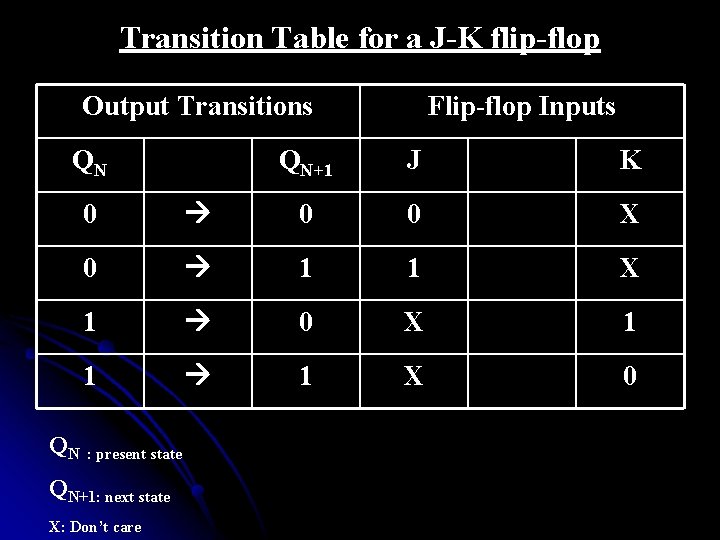
Transition Table for a J-K flip-flop Output Transitions QN QN Flip-flop Inputs QN+1 J K 0 0 0 X 0 1 1 X 1 0 X 1 1 1 X 0 : present state QN+1: next state X: Don’t care

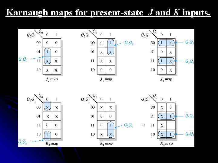
Karnaugh maps for present-state J and K inputs.

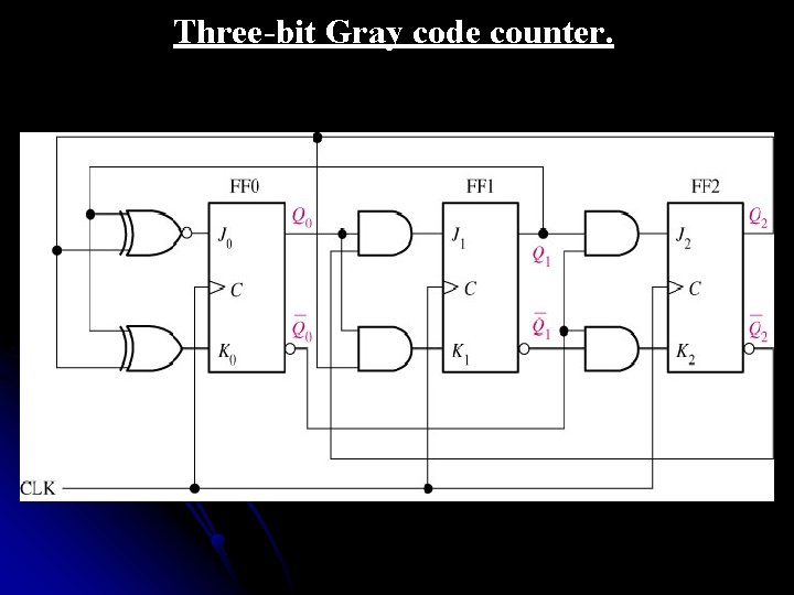
Three-bit Gray code counter.

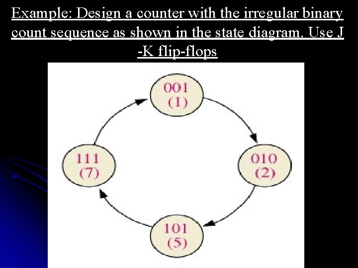
Example: Design a counter with the irregular binary count sequence as shown in the state diagram. Use J -K flip-flops

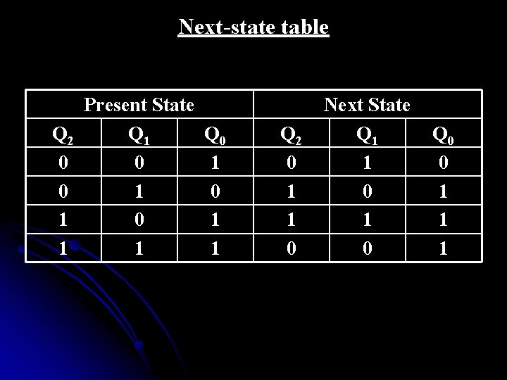
Next-state table Q 2 0 0 1 1 Present State Q 1 0 1 Q 0 1 1 Q 2 0 1 1 0 Next State Q 1 1 0 Q 0 0 1 1 1

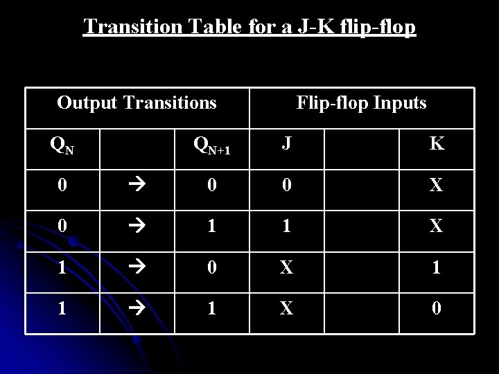
Transition Table for a J-K flip-flop Output Transitions QN Flip-flop Inputs QN+1 J K 0 0 0 X 0 1 1 X 1 0 X 1 1 1 X 0

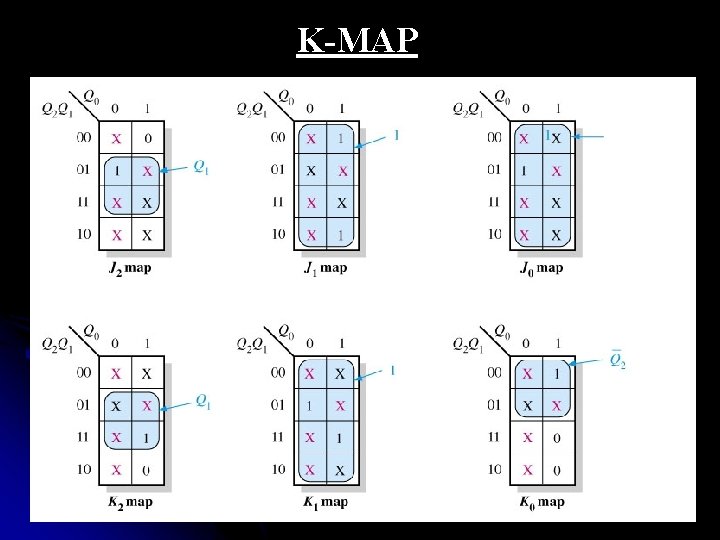
K-MAP

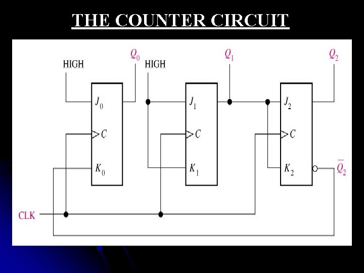
THE COUNTER CIRCUIT

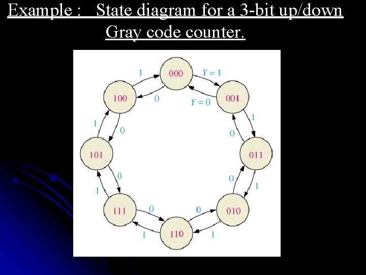
Example : State diagram for a 3 -bit up/down Gray code counter.

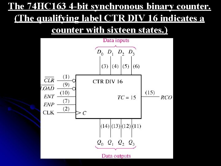
The 74 HC 163 4 -bit synchronous binary counter. (The qualifying label CTR DIV 16 indicates a counter with sixteen states. )

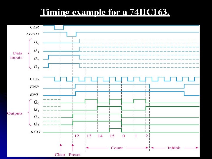
Timing example for a 74 HC 163.

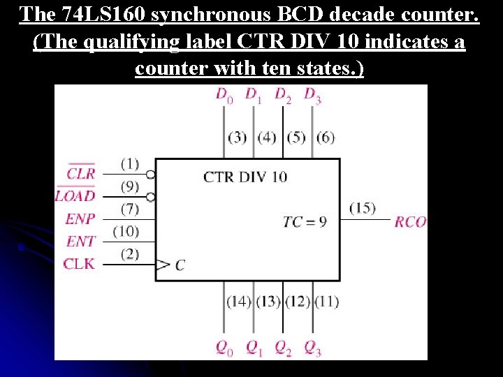
The 74 LS 160 synchronous BCD decade counter. (The qualifying label CTR DIV 10 indicates a counter with ten states. )

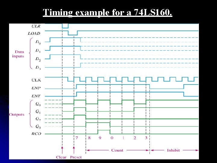
Timing example for a 74 LS 160.

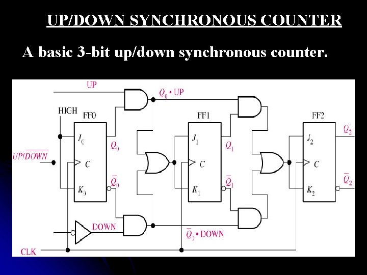
UP/DOWN SYNCHRONOUS COUNTER A basic 3 -bit up/down synchronous counter.

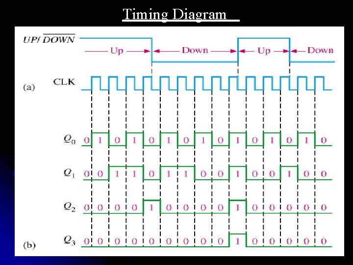
Timing Diagram

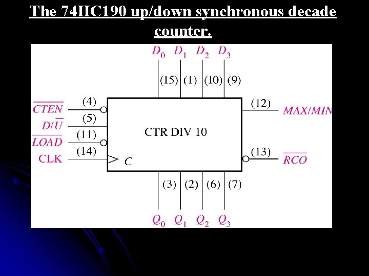
The 74 HC 190 up/down synchronous decade counter.

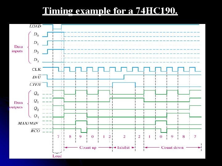
Timing example for a 74 HC 190.

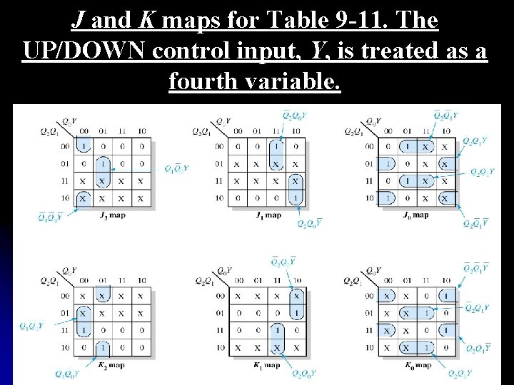
J and K maps for Table 9 -11. The UP/DOWN control input, Y, is treated as a fourth variable.

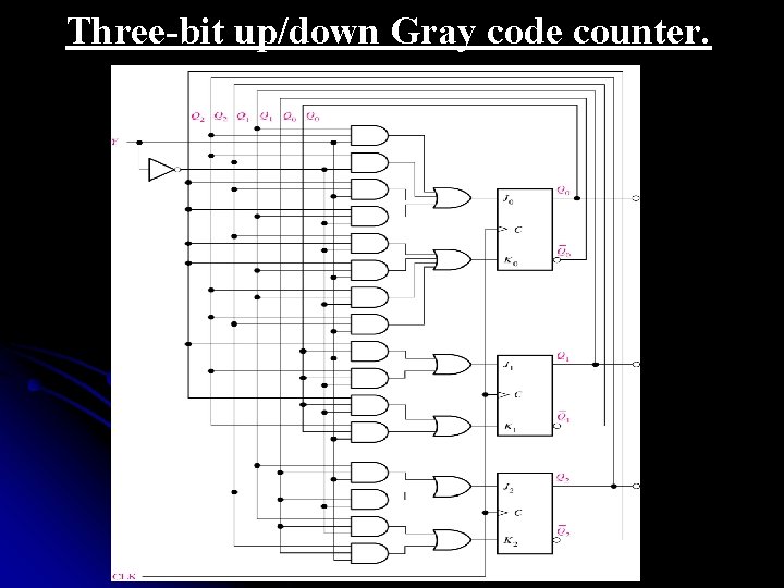
Three-bit up/down Gray code counter.

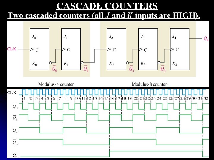
CASCADE COUNTERS Two cascaded counters (all J and K inputs are HIGH).

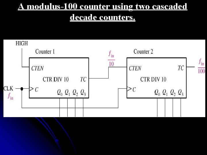
A modulus-100 counter using two cascaded decade counters.

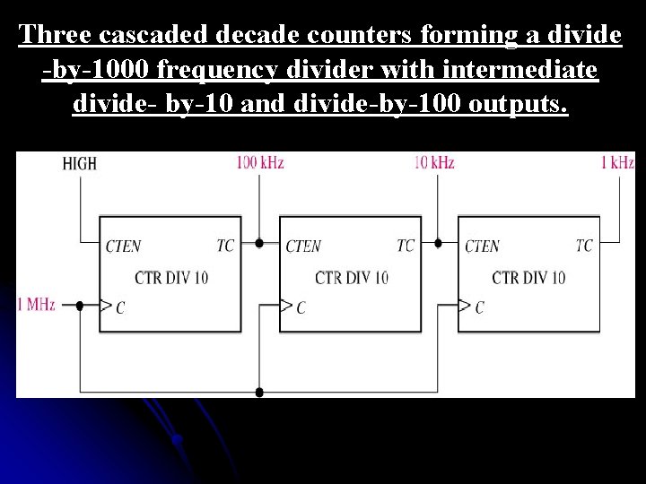
Three cascaded decade counters forming a divide -by-1000 frequency divider with intermediate divide- by-10 and divide-by-100 outputs.

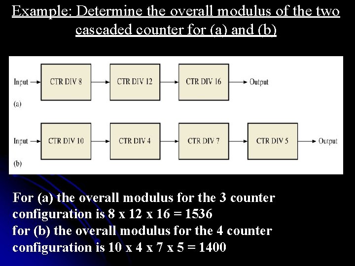
Example: Determine the overall modulus of the two cascaded counter for (a) and (b) For (a) the overall modulus for the 3 counter configuration is 8 x 12 x 16 = 1536 for (b) the overall modulus for the 4 counter configuration is 10 x 4 x 7 x 5 = 1400

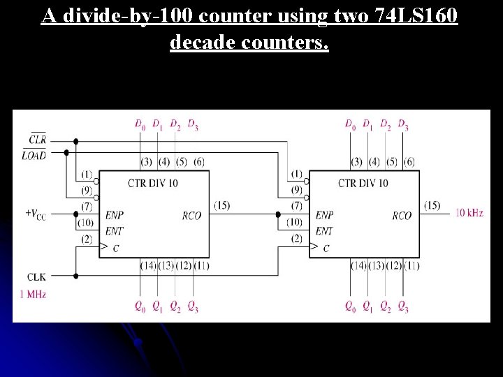
A divide-by-100 counter using two 74 LS 160 decade counters.

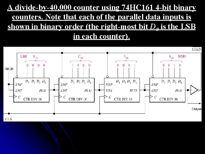
A divide-by-40, 000 counter using 74 HC 161 4 -bit binary counters. Note that each of the parallel data inputs is shown in binary order (the right-most bit D 0 is the LSB in each counter).

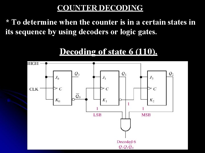
COUNTER DECODING * To determine when the counter is in a certain states in its sequence by using decoders or logic gates. Decoding of state 6 (110).

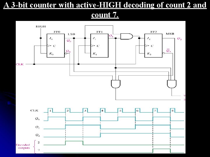
A 3 -bit counter with active-HIGH decoding of count 2 and count 7.

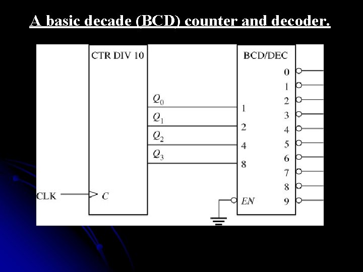
A basic decade (BCD) counter and decoder.

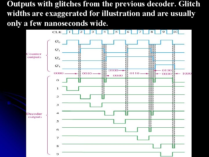
Outputs with glitches from the previous decoder. Glitch widths are exaggerated for illustration and are usually only a few nanoseconds wide.

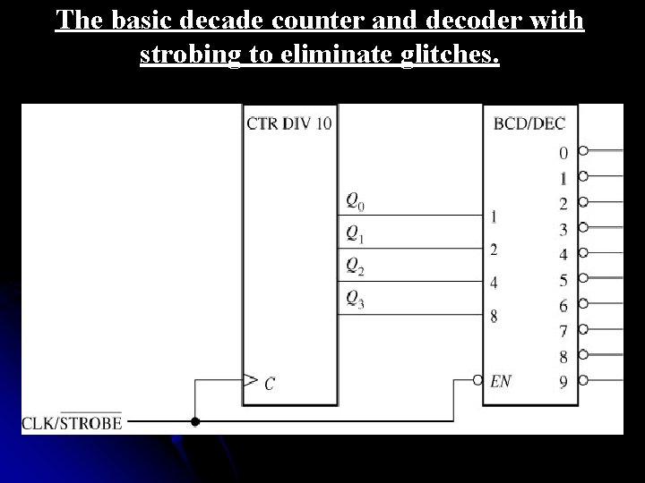
The basic decade counter and decoder with strobing to eliminate glitches.

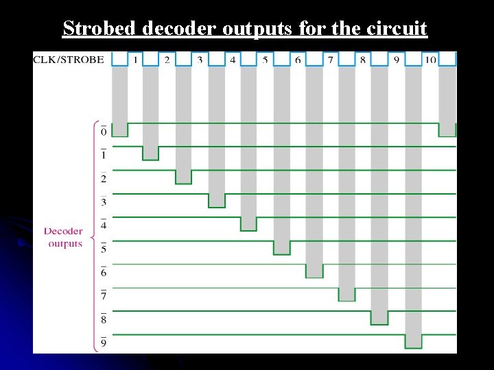
Strobed decoder outputs for the circuit

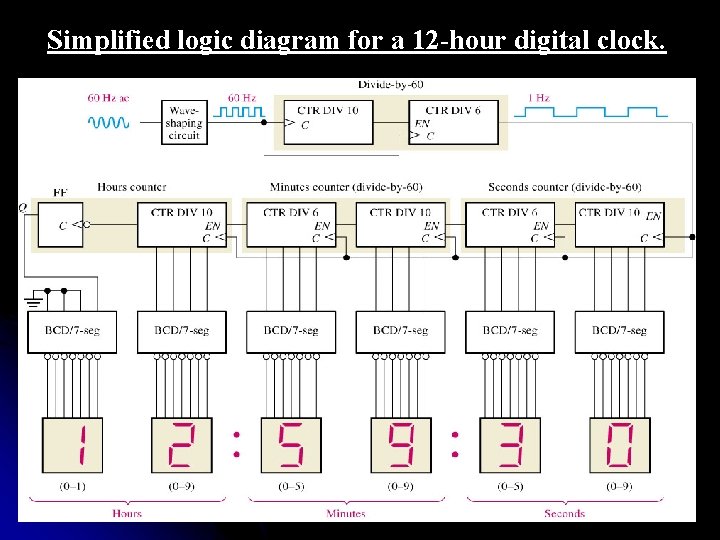
Simplified logic diagram for a 12 -hour digital clock.

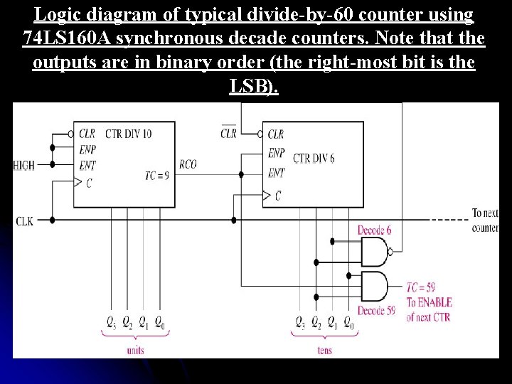
Logic diagram of typical divide-by-60 counter using 74 LS 160 A synchronous decade counters. Note that the outputs are in binary order (the right-most bit is the LSB).

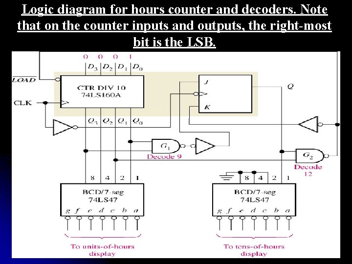
Logic diagram for hours counter and decoders. Note that on the counter inputs and outputs, the right-most bit is the LSB.

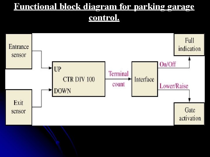
Functional block diagram for parking garage control.

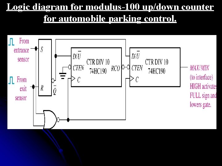
Logic diagram for modulus-100 up/down counter for automobile parking control.

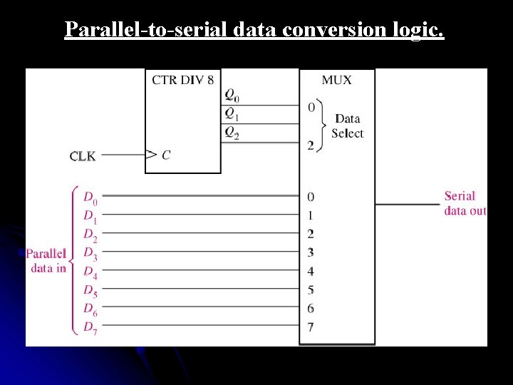
Parallel-to-serial data conversion logic.

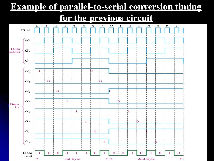
Example of parallel-to-serial conversion timing for the previous circuit

THANK YOU