2 008 Design Manufacturing II Spring 2004 MEMS

![Miller indices • [abc] in a cubic crystal is just a directional vector • Miller indices • [abc] in a cubic crystal is just a directional vector •](https://slidetodoc.com/presentation_image_h2/a2474e58f8f0097e97514c52b784a20b/image-40.jpg)
- Slides: 51

2. 008 Design & Manufacturing II Spring 2004 MEMS I 2. 008 -spring-2004 S. G. Kim

March 10 th �� Ask “Dave” and “Pat” �� Petty money up to $200, Goggles �� Plant tour, April 21, 22, sign up! By 4/2 �� Quiz 1 on March 17 th �� HW#4 due by Monday’s lecture �� 75 minutes (45 min) �� MEMS 1 today 2. 008 -spring-2004 S. G. Kim

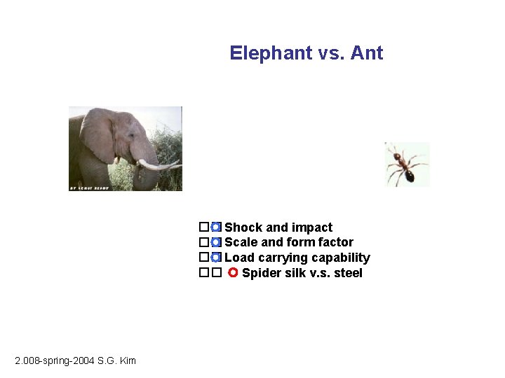
Elephant vs. Ant �� Shock and impact �� Scale and form factor �� Load carrying capability �� Spider silk v. s. steel 2. 008 -spring-2004 S. G. Kim

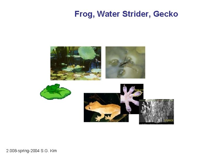
Frog, Water Strider, Gecko 2. 008 -spring-2004 S. G. Kim

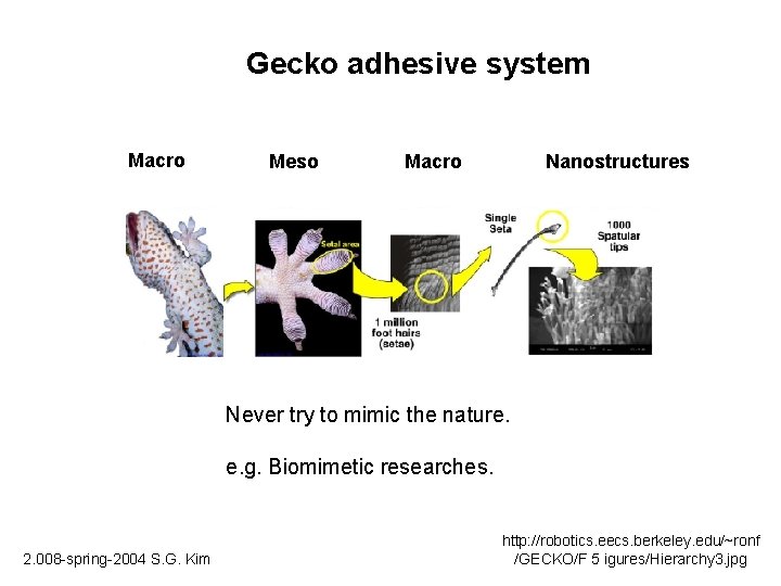
Gecko adhesive system Macro Meso Macro Nanostructures Never try to mimic the nature. e. g. Biomimetic researches. 2. 008 -spring-2004 S. G. Kim http: //robotics. eecs. berkeley. edu/~ronf /GECKO/F 5 igures/Hierarchy 3. jpg

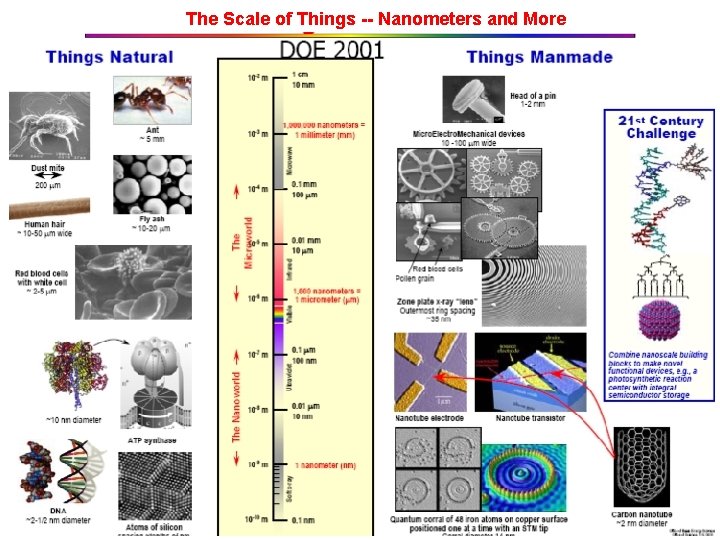
The Scale of Things -- Nanometers and More

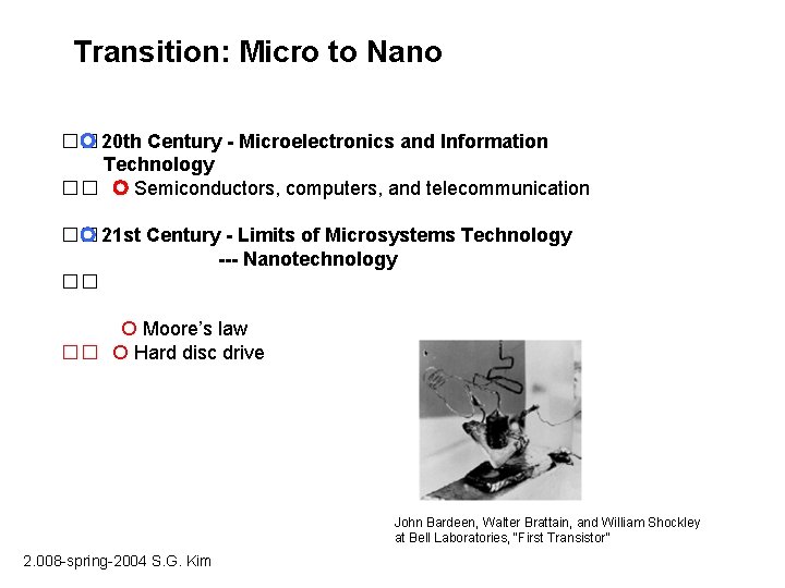
Transition: Micro to Nano �� 20 th Century - Microelectronics and Information Technology �� Semiconductors, computers, and telecommunication �� 21 st Century - Limits of Microsystems Technology --- Nanotechnology �� Moore’s law �� Hard disc drive John Bardeen, Walter Brattain, and William Shockley at Bell Laboratories, “First Transistor” 2. 008 -spring-2004 S. G. Kim

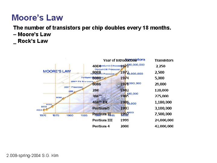
Moore’s Law The number of transistors per chip doubles every 18 months. – Moore’s Law _ Rock’s Law 2. 008 -spring-2004 S. G. Kim

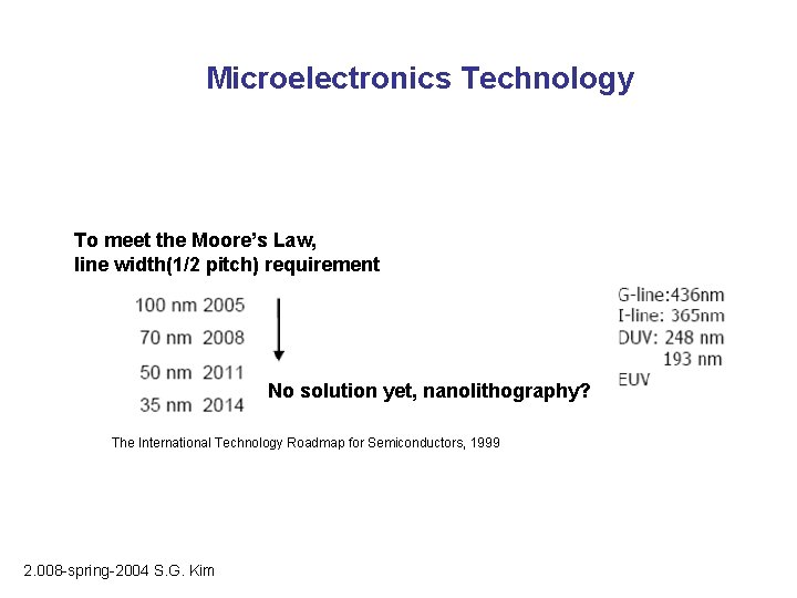
Microelectronics Technology To meet the Moore’s Law, line width(1/2 pitch) requirement No solution yet, nanolithography? The International Technology Roadmap for Semiconductors, 1999 2. 008 -spring-2004 S. G. Kim

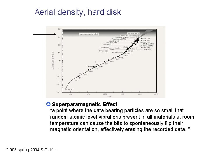
Aerial density, hard disk Superparamagnetic Effect “a point where the data bearing particles are so small that random atomic level vibrations present in all materials at room temperature can cause the bits to spontaneously flip their magnetic orientation, effectively erasing the recorded data. “ 2. 008 -spring-2004 S. G. Kim

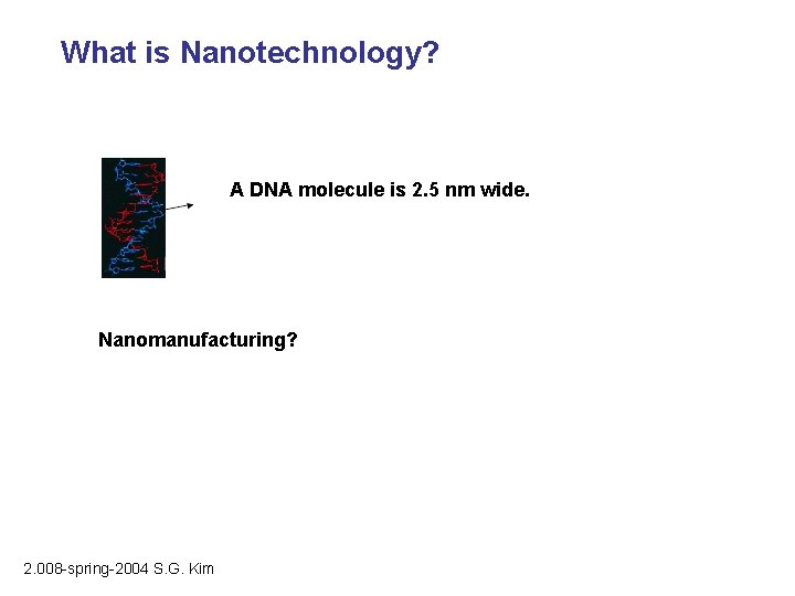
What is Nanotechnology? A DNA molecule is 2. 5 nm wide. Nanomanufacturing? 2. 008 -spring-2004 S. G. Kim

Nano in ME �� Fluidics, heat transfer and energy conversion at the micro- and nanoscale �� Bio-micro-electromechanical systems (bio-MEMS) �� Optical-micro-electromechanical systems (optical. MEMS) �� Engineered nanomaterials �� Nano manufacturing �� Course 2 A (Nanotrack) 2. 008 -spring-2004 S. G. Kim

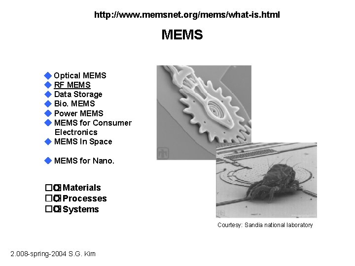
http: //www. memsnet. org/mems/what-is. html MEMS ◆ Optical MEMS ◆ RF MEMS ◆ Data Storage ◆ Bio. MEMS ◆ Power MEMS ◆ MEMS for Consumer Electronics ◆ MEMS In Space ◆ MEMS for Nano. �� Materials �� Processes �� Systems Courtesy: Sandia national laboratory 2. 008 -spring-2004 S. G. Kim

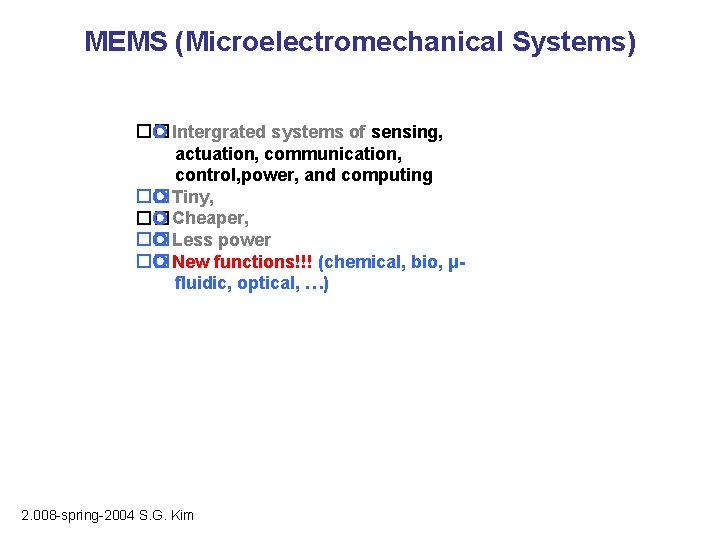
MEMS (Microelectromechanical Systems) �� Intergrated systems of sensing, actuation, communication, control, power, and computing �� Tiny, �� Cheaper, �� Less power �� New functions!!! (chemical, bio, μfluidic, optical, …) 2. 008 -spring-2004 S. G. Kim

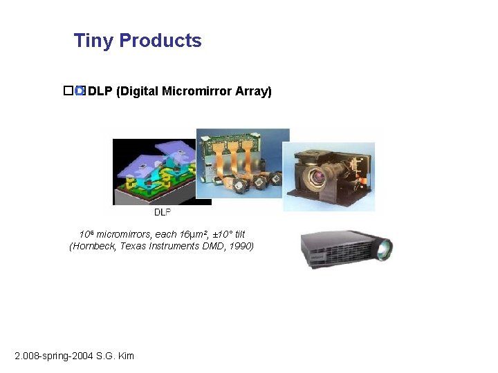
Tiny Products �� DLP (Digital Micromirror Array) 106 micromirrors, each 16μm 2, ± 10° tilt (Hornbeck, Texas Instruments DMD, 1990) 2. 008 -spring-2004 S. G. Kim

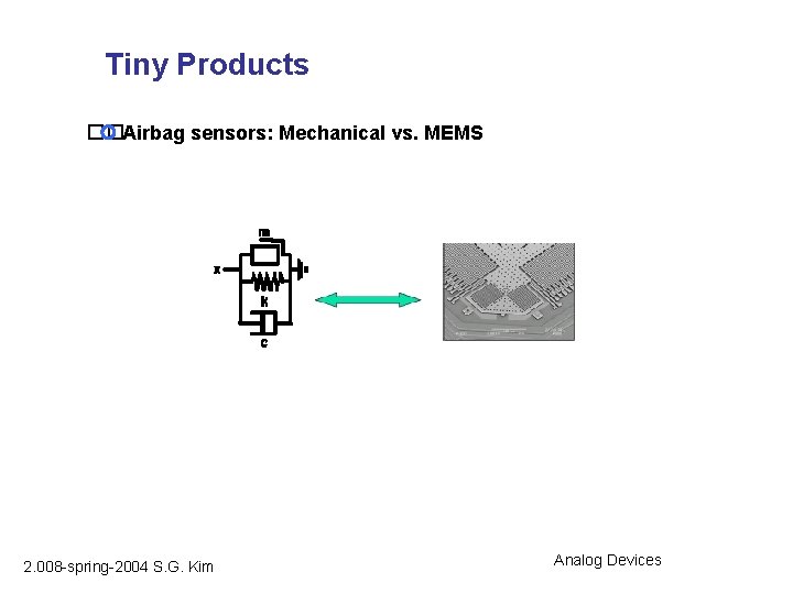
Tiny Products �� Airbag sensors: Mechanical vs. MEMS 2. 008 -spring-2004 S. G. Kim Analog Devices

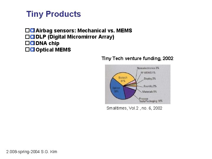
Tiny Products �� Airbag sensors: Mechanical vs. MEMS �� DLP (Digital Micromirror Array) �� DNA chip �� Optical MEMS Tiny Tech venture funding, 2002 Smalltimes, Vol. 2 , no. 6, 2002 2. 008 -spring-2004 S. G. Kim

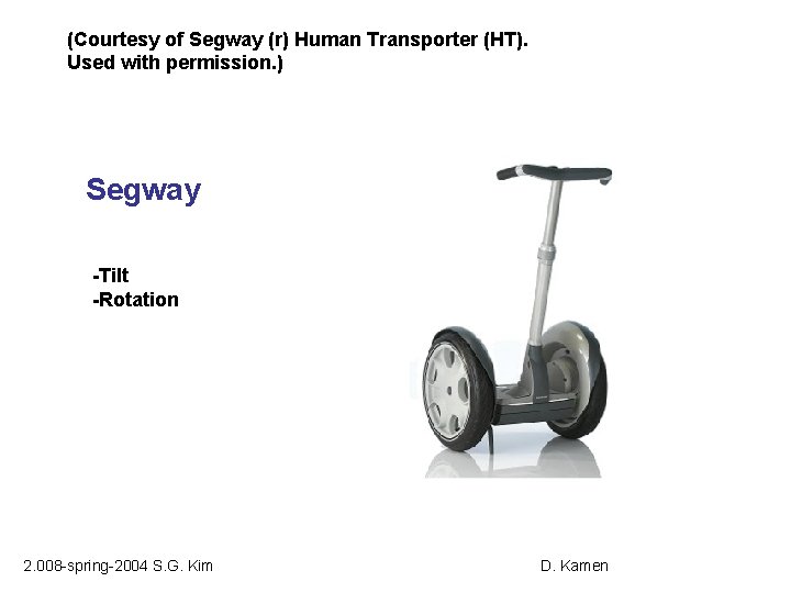
(Courtesy of Segway (r) Human Transporter (HT). Used with permission. ) Segway -Tilt -Rotation 2. 008 -spring-2004 S. G. Kim D. Kamen

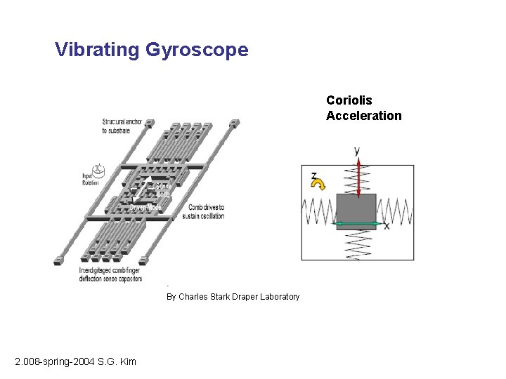
Vibrating Gyroscope Coriolis Acceleration By Charles Stark Draper Laboratory 2. 008 -spring-2004 S. G. Kim

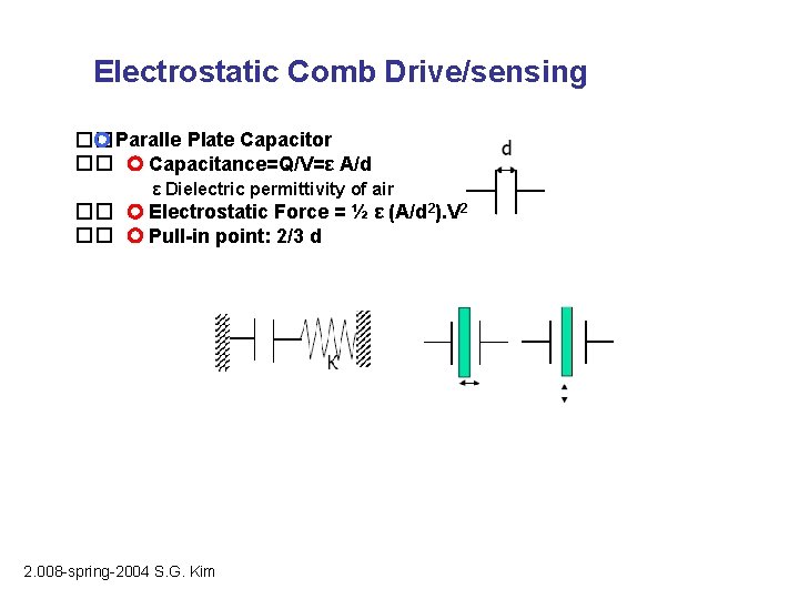
Electrostatic Comb Drive/sensing �� Paralle Plate Capacitor �� Capacitance=Q/V=ε A/d ε Dielectric permittivity of air �� Electrostatic Force = ½ ε (A/d 2). V 2 �� Pull-in point: 2/3 d 2. 008 -spring-2004 S. G. Kim

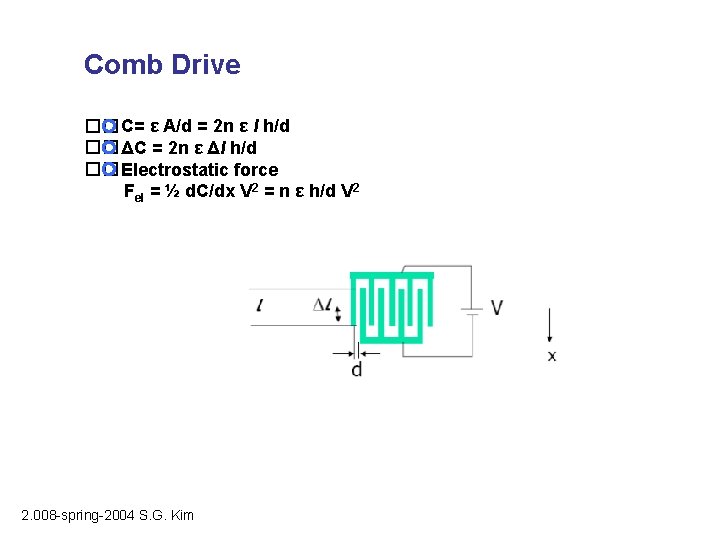
Comb Drive �� C= ε A/d = 2 n ε l h/d �� ΔC = 2 n ε Δl h/d �� Electrostatic force Fel = ½ d. C/dx V 2 = n ε h/d V 2 2. 008 -spring-2004 S. G. Kim

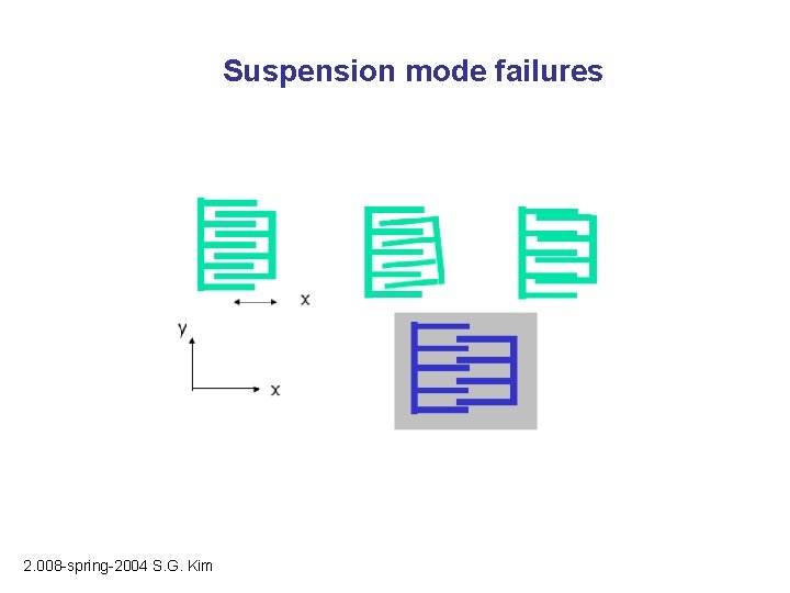
Suspension mode failures 2. 008 -spring-2004 S. G. Kim

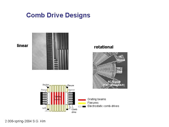
Comb Drive Designs linear rotational Grating beams Flexures Electrostatic comb-drives 2. 008 -spring-2004 S. G. Kim

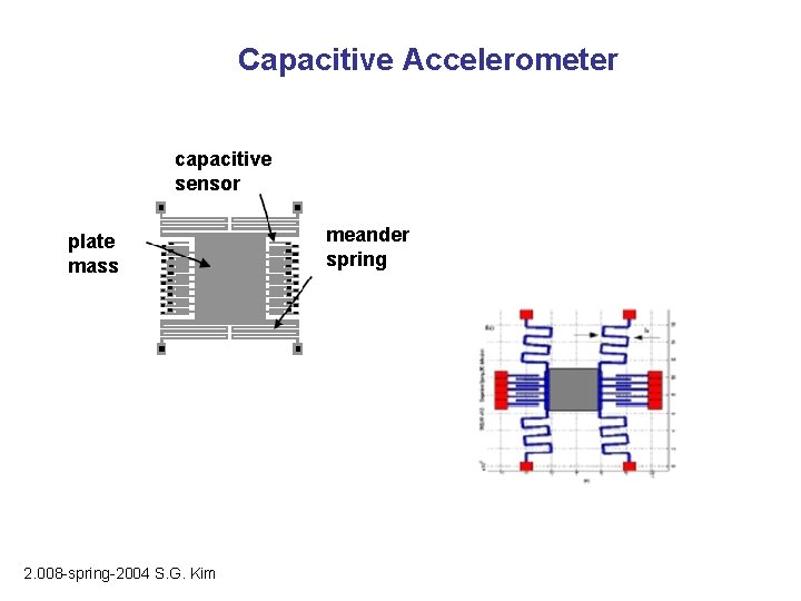
Capacitive Accelerometer capacitive sensor plate mass 2. 008 -spring-2004 S. G. Kim meander spring

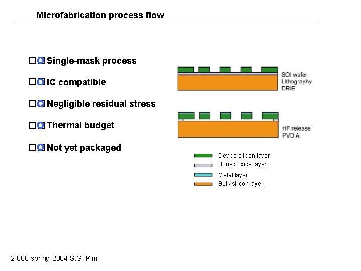
Microfabrication process flow �� Single-mask process �� IC compatible �� Negligible residual stress �� Thermal budget �� Not yet packaged Device silicon layer Buried oxide layer Metal layer Bulk silicon layer 2. 008 -spring-2004 S. G. Kim

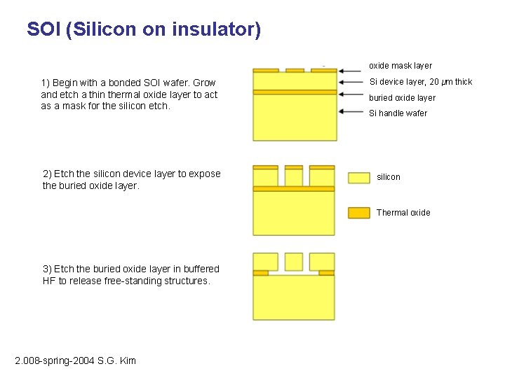
SOI (Silicon on insulator) oxide mask layer 1) Begin with a bonded SOI wafer. Grow and etch a thin thermal oxide layer to act as a mask for the silicon etch. 2) Etch the silicon device layer to expose the buried oxide layer. Si device layer, 20 μm thick buried oxide layer Si handle wafer silicon Thermal oxide 3) Etch the buried oxide layer in buffered HF to release free-standing structures. 2. 008 -spring-2004 S. G. Kim

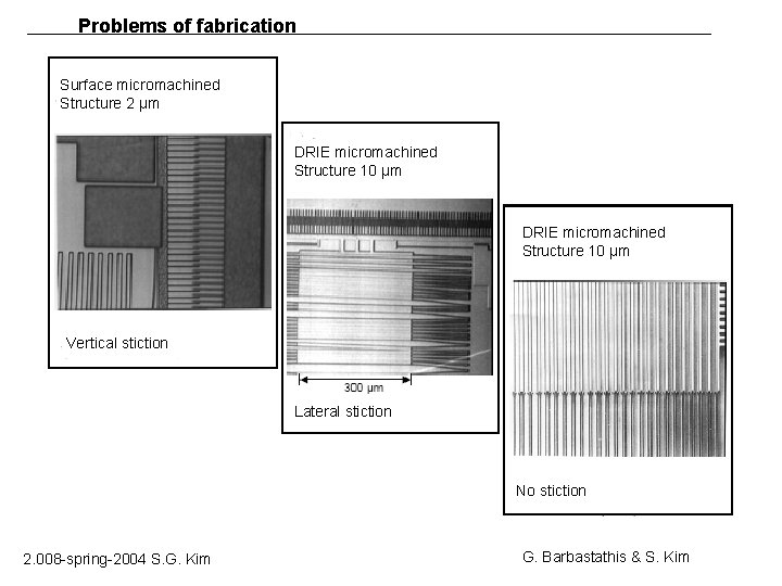
Problems of fabrication Surface micromachined Structure 2 μm DRIE micromachined Structure 10 μm Vertical stiction Lateral stiction No stiction 2. 008 -spring-2004 S. G. Kim G. Barbastathis & S. Kim

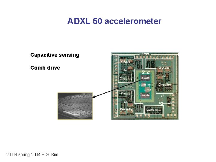
ADXL 50 accelerometer Capacitive sensing Comb drive 2. 008 -spring-2004 S. G. Kim

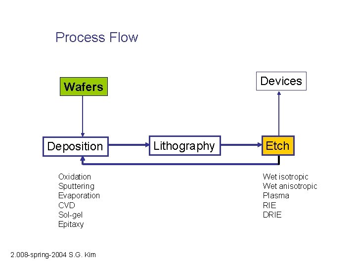
Process Flow Devices Wafers Deposition Oxidation Sputtering Evaporation CVD Sol-gel Epitaxy 2. 008 -spring-2004 S. G. Kim Lithography Etch Wet isotropic Wet anisotropic Plasma RIE DRIE

Micromachining processes • Bulk micromachining • Surface micromachining • Bonding • LIGA • x-ray lithography, electrodeposition and molding 2. 008 -spring-2004 S. G. Kim

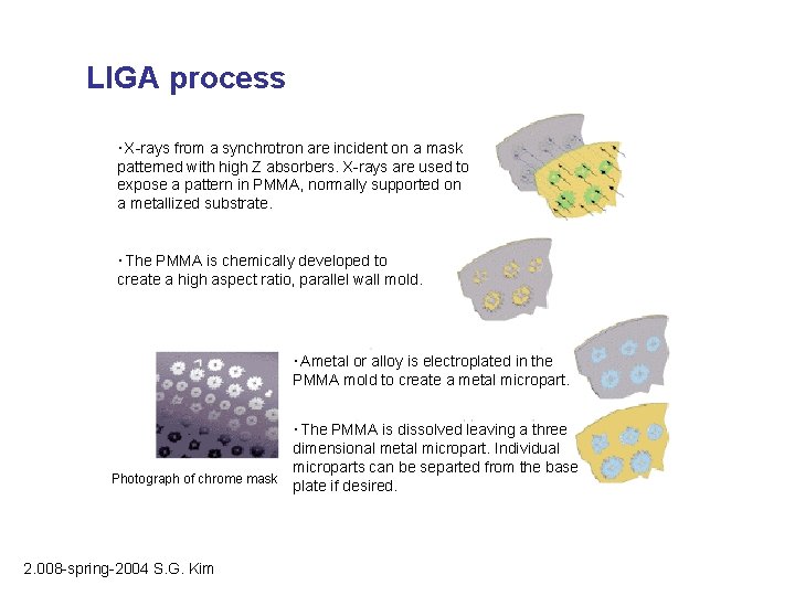
LIGA process ‧X-rays from a synchrotron are incident on a mask patterned with high Z absorbers. X-rays are used to expose a pattern in PMMA, normally supported on a metallized substrate. ‧The PMMA is chemically developed to create a high aspect ratio, parallel wall mold. ‧Ametal or alloy is electroplated in the PMMA mold to create a metal micropart. ‧The PMMA is dissolved leaving a three dimensional metal micropart. Individual microparts can be separted from the base Photograph of chrome mask plate if desired. 2. 008 -spring-2004 S. G. Kim

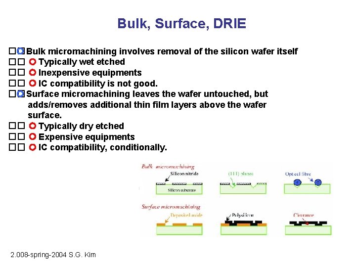
Bulk, Surface, DRIE �� Bulk micromachining involves removal of the silicon wafer itself �� Typically wet etched �� Inexpensive equipments �� IC compatibility is not good. �� Surface micromachining leaves the wafer untouched, but adds/removes additional thin film layers above the wafer surface. �� Typically dry etched �� Expensive equipments �� IC compatibility, conditionally. 2. 008 -spring-2004 S. G. Kim

Materials �� Metals �� Al, Au, ITO, W, Ni, Ti. Ni, … �� Insulators �� Si. O 2 - thermally grown above 800 o. C or vapor deposited (CVD), sputtered. Large intrinsic stress �� Six. Ny – insulator, barrier for ion diffusion, high E, stress controllable �� Polymers: PR, SU-8, PDMS �� Glass, quartz �� Silicon �� stronger than steel, lighter than aluminum �� single crystal, polycrystalline, or amorphous 2. 008 -spring-2004 S. G. Kim

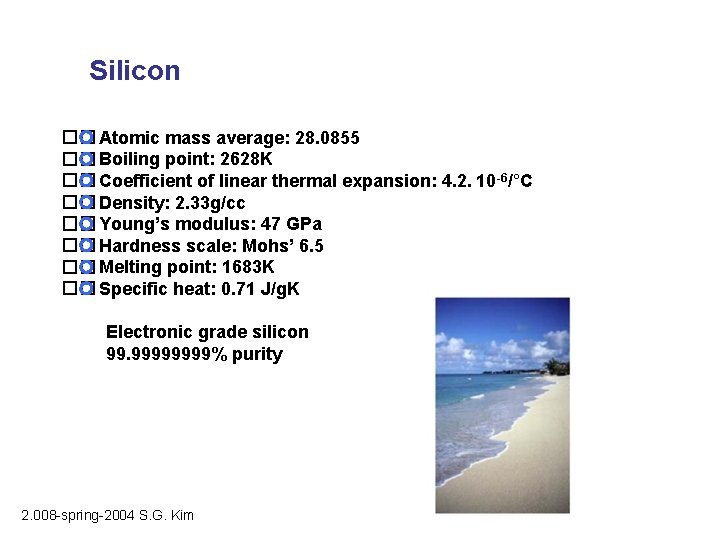
Silicon �� Atomic mass average: 28. 0855 �� Boiling point: 2628 K �� Coefficient of linear thermal expansion: 4. 2. 10 -6/°C �� Density: 2. 33 g/cc �� Young’s modulus: 47 GPa �� Hardness scale: Mohs’ 6. 5 �� Melting point: 1683 K �� Specific heat: 0. 71 J/g. K Electronic grade silicon 99. 9999% purity 2. 008 -spring-2004 S. G. Kim

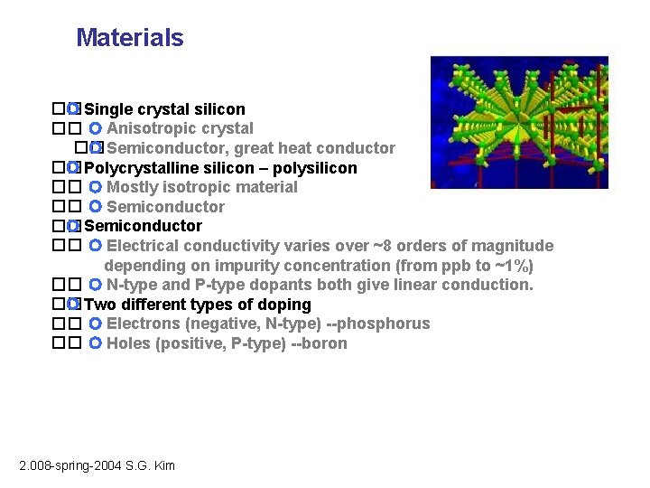
Materials �� Single crystal silicon �� Anisotropic crystal �� Semiconductor, great heat conductor �� Polycrystalline silicon – polysilicon �� Mostly isotropic material �� Semiconductor �� Electrical conductivity varies over ~8 orders of magnitude depending on impurity concentration (from ppb to ~1%) �� N-type and P-type dopants both give linear conduction. �� Two different types of doping �� Electrons (negative, N-type) --phosphorus �� Holes (positive, P-type) --boron 2. 008 -spring-2004 S. G. Kim

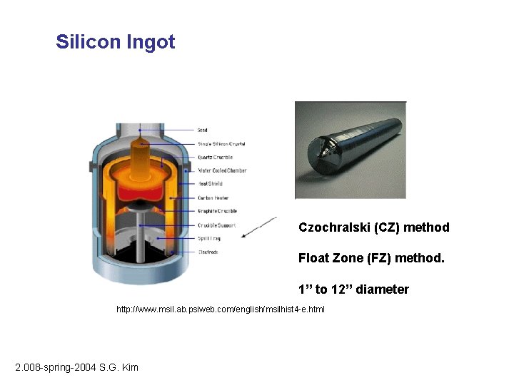
Silicon Ingot Czochralski (CZ) method Float Zone (FZ) method. 1” to 12” diameter http: //www. msil. ab. psiweb. com/english/msilhist 4 -e. html 2. 008 -spring-2004 S. G. Kim

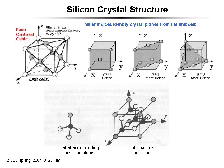
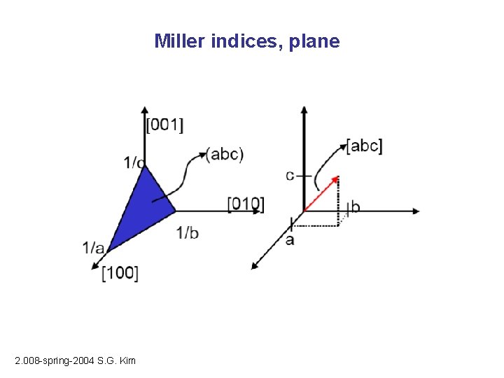
Silicon Crystal Structure Miller indices identify crystal planes from the unit cell: Tetrahedral bonding of silicon atoms 2. 008 -spring-2004 S. G. Kim Cubic unit cell of silicon

Miller indices, plane 2. 008 -spring-2004 S. G. Kim

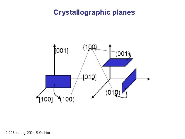
Crystallographic planes 2. 008 -spring-2004 S. G. Kim
![Miller indices abc in a cubic crystal is just a directional vector Miller indices • [abc] in a cubic crystal is just a directional vector •](https://slidetodoc.com/presentation_image_h2/a2474e58f8f0097e97514c52b784a20b/image-40.jpg)
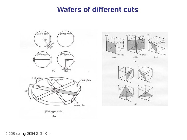
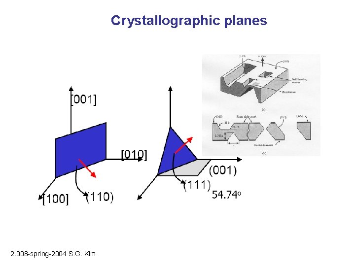
Miller indices • [abc] in a cubic crystal is just a directional vector • (abc) is any plane perpendicular to the [abc] vector • (…)/[…] indicate a specific plane/direction • {…}/<…> indicate equivalent set of planes/directions 2. 008 -spring-2004 S. G. Kim

Wafers of different cuts 2. 008 -spring-2004 S. G. Kim

Crystallographic planes 2. 008 -spring-2004 S. G. Kim

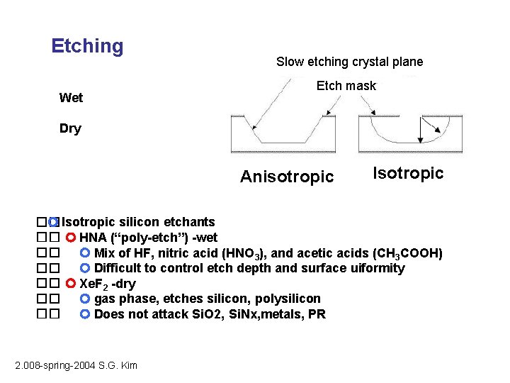
Etching Wet Slow etching crystal plane Etch mask Dry Anisotropic Isotropic �� Isotropic silicon etchants �� HNA (“poly-etch”) -wet �� Mix of HF, nitric acid (HNO 3), and acetic acids (CH 3 COOH) �� Difficult to control etch depth and surface uiformity �� Xe. F 2 -dry �� gas phase, etches silicon, polysilicon �� Does not attack Si. O 2, Si. Nx, metals, PR 2. 008 -spring-2004 S. G. Kim

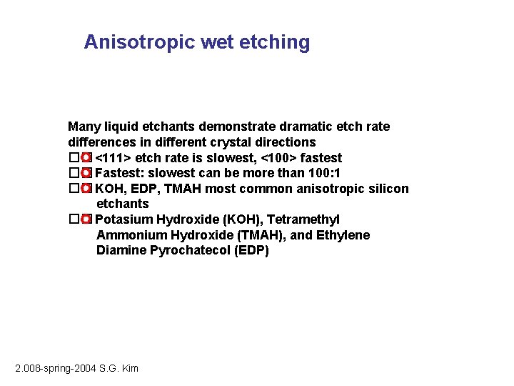
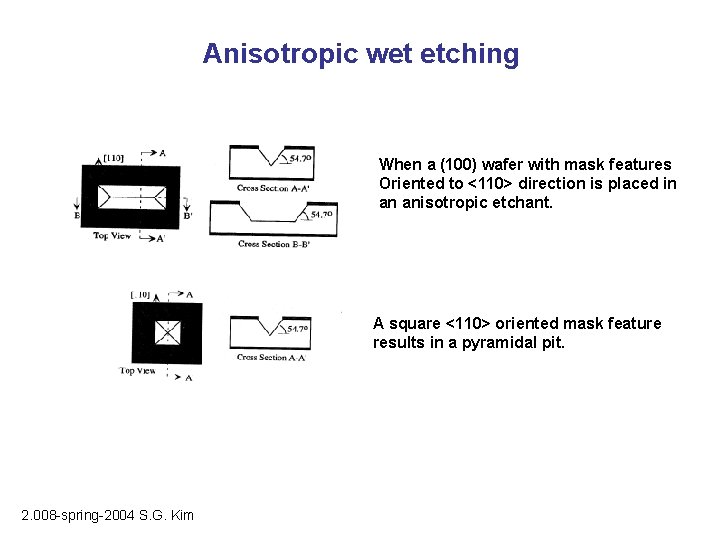
Anisotropic wet etching Many liquid etchants demonstrate dramatic etch rate differences in different crystal directions �� <111> etch rate is slowest, <100> fastest �� Fastest: slowest can be more than 100: 1 �� KOH, EDP, TMAH most common anisotropic silicon etchants �� Potasium Hydroxide (KOH), Tetramethyl Ammonium Hydroxide (TMAH), and Ethylene Diamine Pyrochatecol (EDP) 2. 008 -spring-2004 S. G. Kim

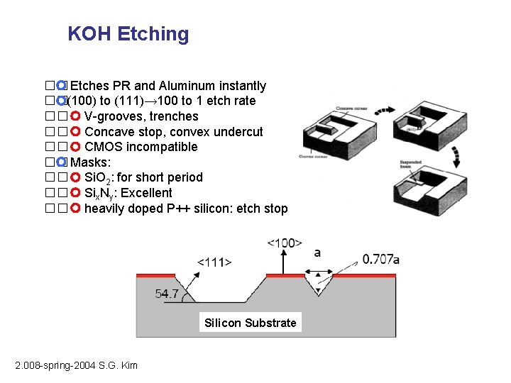
KOH Etching �� Etches PR and Aluminum instantly �� (100) to (111)→ 100 to 1 etch rate �� V-grooves, trenches �� Concave stop, convex undercut �� CMOS incompatible �� Masks: �� Si. O 2: for short period �� Six. Ny: Excellent �� heavily doped P++ silicon: etch stop Silicon Substrate 2. 008 -spring-2004 S. G. Kim

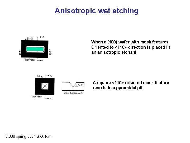
Anisotropic wet etching When a (100) wafer with mask features Oriented to <110> direction is placed in an anisotropic etchant. A square <110> oriented mask feature results in a pyramidal pit. 2. 008 -spring-2004 S. G. Kim

Anisotropic wet etching When a (100) wafer with mask features Oriented to <110> direction is placed in an anisotropic etchant. A square <110> oriented mask feature results in a pyramidal pit. 2. 008 -spring-2004 S. G. Kim

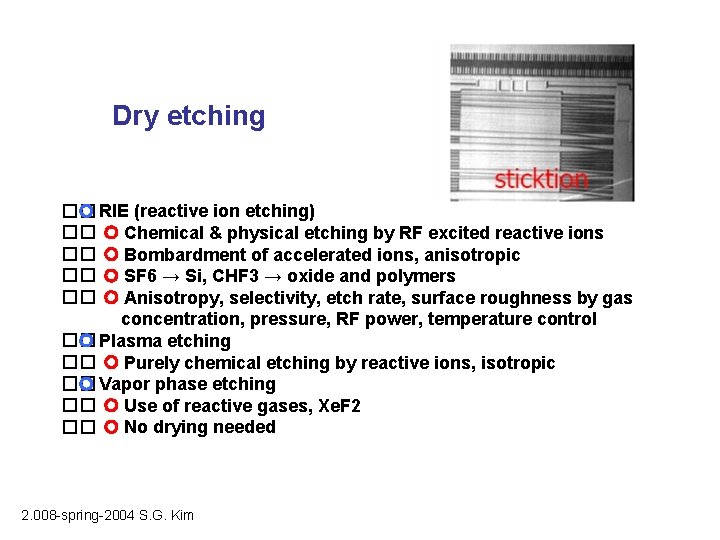
Dry etching �� RIE (reactive ion etching) �� Chemical & physical etching by RF excited reactive ions �� Bombardment of accelerated ions, anisotropic �� SF 6 → Si, CHF 3 → oxide and polymers �� Anisotropy, selectivity, etch rate, surface roughness by gas concentration, pressure, RF power, temperature control �� Plasma etching �� Purely chemical etching by reactive ions, isotropic �� Vapor phase etching �� Use of reactive gases, Xe. F 2 �� No drying needed 2. 008 -spring-2004 S. G. Kim

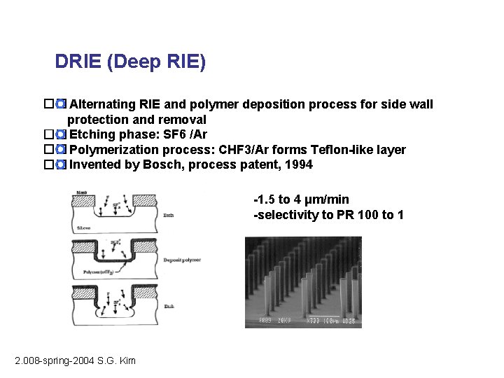
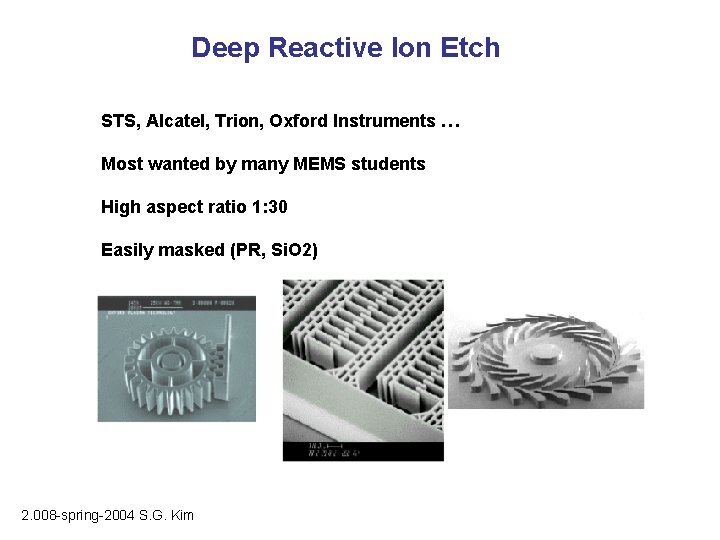
DRIE (Deep RIE) �� Alternating RIE and polymer deposition process for side wall protection and removal �� Etching phase: SF 6 /Ar �� Polymerization process: CHF 3/Ar forms Teflon-like layer �� Invented by Bosch, process patent, 1994 -1. 5 to 4 μm/min -selectivity to PR 100 to 1 2. 008 -spring-2004 S. G. Kim

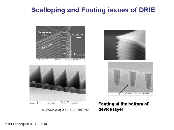
Scalloping and Footing issues of DRIE Milanovic et al, IEEE TED, Jan. 2001. 2. 008 -spring-2004 S. G. Kim Footing at the bottom of device layer

Deep Reactive Ion Etch STS, Alcatel, Trion, Oxford Instruments … Most wanted by many MEMS students High aspect ratio 1: 30 Easily masked (PR, Si. O 2) 2. 008 -spring-2004 S. G. Kim