EMT 452 MEMS SEMESTER II 20102011 MEMS Packaging


 Sealing by chemical reactions: Sealing • Sealing is accomplished by “growing” the sealant")


 is the most common of all")


 By coating with silicone gel: ● Silicone gel containing one or two parts")
 Indirect pressure transmission: ● This method is used in situation in")
 applications of micropump.")
- Slides: 52
EMT 452 MEMS SEMESTER II 2010/2011 MEMS Packaging
Outlines • • • Introduction Key Design and Packaging Considerations Three Levels of MEMS Packaging Interfaces in Microsystems Packaging Enabling Packaging Technologies – – Die Preparation Surface Bonding / Die-Attach Processes Wire Bonding Sealing • Types of Packaging Solutions – Ceramic Packaging – Metal Packaging – Molded Plastic Packaging • Quality Control, Reliability, and Failure Analysis – Quality Control and Reliability Standards – Statistical Methods in Reliability – Accelerated Life Modeling – Major Failure Modes
Introduction • Packaging is the process, industry, and methods of “packing” microelectromechanical components and systems inside a protective housing. • It converts a micromachined structure or system into a useful assembly that can safely and reliably interact with its surroundings. • Electronic packaging: - Reliable dense interconnections to the multitude of high-frequency electrical signals - Extract excessive heat from the chips.
Introduction • MEMS packaging: - must account for a complex and diverse set of parameters - must protect the micromachined parts in broad-ranging environments - must provide interconnects to electrical signals and, in most cases, access to and interaction with the external environment.
Introduction • For example, the packaging of a pressure sensor must ensure that the sensing device is in intimate contact with the pressurized medium yet protected from exposure to any harmful substances in this medium.
Key Design and Packaging Considerations • Designing packages for micromachined sensors and actuators involves a number of important factors. • Some are shared with the packaging of electronic integrated circuits, but many are specific to the application. • These factors also bear significance on the design of the micromachined components themselves. • As a result, the design of the package and of the micromachined structures must commence and evolve together.
Figure 8. 1 A simplified process flow for MEMS packaging. 1. Upon completion of wafer-level fabrication, inspection and first tests take place. 2. The wafer is then mounted on a special sticky tape and sawed. The individual dice are separated. Some post processing, such as removal of a sacrificial layer, may occur at this point. One die or many dice are attached to a ceramic, a metal header, or a premolded plastic lead frame. 3. Electrical interconnects are made by wire bonding, flip chip, or another method. 4. A ceramic, metal, glass, or plastic cap seals the assembly. Alternatively, the die or dice are attached to a metal lead frame. 5. After the electrical interconnects are made, plastic is molded over the assembly. A final test and calibration conclude the process. This simple process does not allow for fluidic or optical connections.
Critical factors and considerations in MEMS packaging ● The required costs in manufacturing, assemblies and packaging of the components. ● The expected environmental effects, such as temperature, humidity, chemical toxicity, etc. that the product is designed for. ● Adequate over capacity in the packaging design for mishandling and accidents. ● Proper choice of materials for the reliability of the package. ● Achieving minimum electrical feed-through and bonds in order to minimize the probability of wire breakage and malfunctioning.
Three levels of MEMS packaging Level 1: The “die level”, Level 2: The “device level”, Level 3: The “system level”.
Die-level packaging Dies in most microsystems are the most delicate components, which require adequate protection. The objectives of this level packaging are: ● To protect the die or other core elements from plastic deformation and cracking, ● To protect the active circuitry for signal transduction of the system, ● To provide necessary mechanical isolation of these elements, and ● To ensure the system functioning at both normal operating and over- load conditions. This level involves wire bonds for electronic signal transmission and transduction such as the embedded piezoresistors in a pressure sensor die and the circuits that connect to them.
Die-level packaging often involves wire bonding:
Device-level packaging Major interface problems: • The interfaces of delicate dies and core elements with other parts of the packaged products at radically different sizes • The interfaces of these delicate elements with environmental factors, such as temperature, pressure and toxicity of the working and the contacting media.
System-level packaging ● Involves the packaging of primary signal circuitry with the package of the die or core element unit. ● Major tasks involve proper mechanical and thermal isolation as well as electromagnetic shielding of the circuitry. ● Metal housings usually give excellent protection for mechanical and electromagnetic influences. ● MEMS devices or microsystems at the end of this packaging level are ready to be “plug-in” to the existing engineering systems.
Interfaces in Microsystems Packaging ● Various parts, in particular, the delicate dies of microsystems are expected to be in contact with various working media, e. g. chemicals, optical, corrosive gases, etc. ● Interface between these parts with working media becomes a major design issue in packaging.
Biomedical interfaces • The packaged systems need to be biologically compatible with human systems and they are expected to function for a specified lifetime. • Every micro biosystem must be built to satisfy the following requirements that are related to interface: 1. It is inert to chemical attack during the useful lifetime of the unit. 2. It follows mixing with biological materials in a well-controlled manner if it is used as biosensors. 3. It causes no damage or harm to the surrounding biological cells in the cases of instrumented catheters such as pace makers. 4. It causes no unwanted chemical reactions such as corrosion between the packaged device and the contacting human body fluids, tissue and cells.
Optical interfaces • There are two principal types of optical MEMS: 1. The direction of the lights in devices, e. g. micro switches involving mirrors and reflectors. 2. Optical sensors.
• Optical MEMS require: – Proper passages for light beams to be received and reflected. – Proper surface coating for receiving and reflect lights. – The quality of the coating must be enduring the lifetime of the device. – The surfaces must be free of contamination of foreign substance. – The enclosure must be free of moisture. The presence of moisture may cause stiction of the enclosed components.
Electromechanical interface • Electrical insulation, grounding and shielding are typical problems to be dealt with in MEMS and microsystems packaging.
Interfaces in microfluidics – Require precise fluid delivery, hermal and environmental isolation and mixing. – Material compatibility of microchannel and contained solvent – Major interface problems: § sealing of the fluid § interface between the contacting channel walls and fluid containment wall
Enabling Packaging Technologies Die preparation • Dies, or substrates in MEMS, are normally cut (sliced) from single wafers using thin diamond saw blades. Spacing between dies: ≈ 50 μm with saw blade thickness of 20 μm. Cutting wheel: 75 – 100 mm diameter Cutting speed: 30, 000 – 40, 000 rpm.
Die-Attach / Surface Bonding Processes • After wafer dicing, each individual die is mounted inside a package and attached (bonded) onto a platform made of metal or ceramic, though plastic is also possible under limited circumstances. There are four (4) techniques available for surface bonding in MEMS and microsystems: (1) Adhesives (2) Eutectic soldering (3) Anodic bonding (4) Silicon fusion bonding (SFB)
Bonding by adhesives ● Epoxy resin and silicone rubbers are two commonly used adhesives. ● Good bonding by epoxy resin rely on surface treatments and curing process control. Avoid glass transition temperature at 150 -175 o. C. ● Soft silicone rubbers are used for bonding parts require “flexibility. ” It is vulnerable to chemicals and air.
Eutectic bonding • Eutectic bonding involves the diffusion of atoms of eutectic alloys into the atomic structures of the materials to be bonded together. • Must first select a candidate material that will form a eutectic alloy with the materials to be bonded. • A common material to form eutectic alloy with silicon is thin films made of gold or alloys that involve gold. • Gold-tin (80% Au+20% Sn) films around 25 μm thick is commonly used. • Bonding takes place at about 300 o. C. • Offers much solid bonding than adhesives.
Anodic bonding Bonding wafers of different materials. Also called “electrostatic bonding” or “Field-assisted thermal bonding. ” It is popular because of simple set-up and inexpensive equipment. Bonding temperature is relatively low in the range: 180500 o. C. Possible to bond wafers of: Glass-to-glass, Glass-to-silicon compounds, Glass-to-Metals and Silicon-to-silicon Most common application is for Glass-to-silicon wafer bonding. :
Anodic bonding The working principle of Glass-to-silicon wafer bonding:
Silicon Fusion bonding ● Silicon fusion bonding is like “welding” a silicon wafer to another silicon wafer. ● It is relatively simple and inexpensive bonding method. ● Silicon fusion bonding (SFB) has been used to bond: – Silicon-to-silicon, Silicon with oxide-to silicon with oxide, Ga. As-tosilicon, Quartz-to-silicon and Silicon-to-glass
Silicon Fusion bonding ● It is the induced chemical forces that bond the pieces together. ● Wafer surfaces need to be extremely flat (at 4 nm) to be bonded. ● Bonding strength between silicon wafers can be as high as 20 MPa. ● The SFB process begins with thorough cleaning of the bonding surfaces. These surfaces must be polished, then make them hydrophilic by exposing them in boiling nitric acid. ● These two surfaces are naturally bonded even at room temperature. ● Strong bonding occurs at high temperature in the neighborhood of 1100 o. C to 1400 o. C.
Wire Bonding • Wire bonding techniques provides the electrical connection to or from the core elements.
Thermocompression wire bonding ● Wire bonding is accomplished with mechanical compression at elevated temperatures at about 400 o. C. ● The bonding process is illustrated as: – Heat the wire to form a bead – Feed the bead to the pad by pulling down the capillary tool:
Wedge-wedge ultrasonic bonding ● This bonding process takes place at room temperature. ● The energy supply to the bonding is from ultrasonic vibration of the tool at 20 – 60 k. Hz. ● The process is illustrated as: Thermosonic bonding ● This process uses ultrasonic energy with thermocompression. ● As such, wire bonding can take place at 100 -150 o. C. ● Joints can be in either ball-wedge or wedge-wedge form.
Sealing • Sealing is a key requirement in MEMS and microsystems packaging. • Hermetic sealing is essential in devices or systems such as: microfluidic, opto. MEMS, bio. MEMS, pressure sensors, etc. • There are generally 3 sealing techniques available for MEMS and microsystems: (1) Mechanical sealing technique: • Epoxy for microfluidics. It is flexible but ages with time. ● Eutectic soldering for hermetic seals. (2) Sealing by microfabrication processes - Sealing by micro shells:
(3) Sealing by chemical reactions: Sealing • Sealing is accomplished by “growing” the sealant using chemical reactions. • Example is the production of Si. O 2 as the sealant for sealing a delicate die with a silicon shell. • The growth of Si. O 2 from the silicon encapsulant to the constraint base provides reliable and hermetic seal for the die
Types of Packaging • A package is a protective housing with an enclosure to hold one or multiple dice forming a complete microelectromechanical device or system. • The package provides where necessary electrical, optical, and fluid connectivity between the dice and the external world • There are three general categories of widely adopted packaging approaches in MEMS; ceramic, metal, and plastic.
Ceramic Packaging • Ceramics are hard and brittle materials made by shaping a nonmetallic mineral, then firing at a high temperature for densification. • The vast majority of ceramics are electrical insulators and often are good thermal conductors. • Ease of shaping along with reliability and attractive material properties (e. g. , electrical insulator, hermetic sealing) have made ceramics a mainstay in electronic packaging. They are widely used in multichip modules (MCM) [19] and advanced electronic packages such as ball grid arrays (BGA) [20].
Ceramic Packaging • Many commercially available micromachined sensors use some form of ceramic packaging. • Ceramics are completely customizable and allow the formation of through ports and manifolds for the packaging of fluid-based MEMS. Ceramics usually suffer from shrinkage (~13% in the horizontal direction and ~15% in the vertical direction) during firing, which manufacturers take into account in their designs. • Ceramic are significantly more expensive compared to plastic packaging.
Ceramic Packaging • Alumina (Al 2 O 3) is the most common of all ceramics, having been used over the centuries in porcelain and fine dinnerware. • Aluminum nitride (Al. N) and beryllia (Be. O) have superior material properties (e. g. , better thermal conductivity), but the latter is very toxic. • Aluminum nitride substrates tend to be costly in particular because of required complex processing due to the difficulty of sintering the material.
A ceramic package is made of laminates, each formed and patterned separately, then brought together and cofired (sintered) at an elevated temperature—typically between 1, 500ºC and 1, 600ºC.
Metal Packaging • In the early days of the integrated circuit industry, the number of transistors on a single chip and the corresponding pin count (number of I/O connections) were few. • Metal packages were practical because they were robust and easy to assemble. The standard family of transistor outline (TO)-type packages grew to cover a wide range of shapes, but all accommodated fewer than 10 electrical pins. • But the semiconductor industry abandoned the TO packages in favor of plastic and ceramic packaging as the density of transistors grew exponentially and the required pin count increased correspondingly. TO-type packages remain in use for few applications, in particular high-power discrete devices and highvoltage linear circuits (e. g. , operational amplifiers).
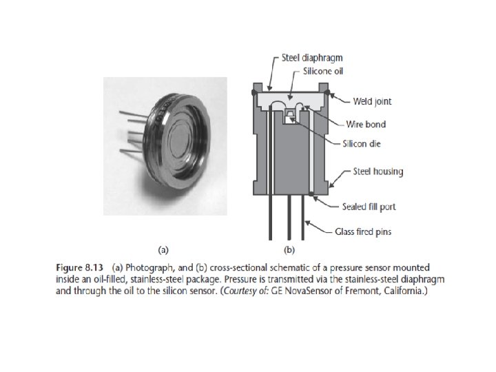
Metal Packaging • Metal packages are attractive to MEMS for the same reasons the integrated circuit industry adopted the technology over 30 years ago. • They satisfy the pin count requirements of most MEMS applications; - they can be prototyped in small volumes with rather short turnaround periods - they are hermetic when sealed. • But a major disadvantage is the relatively large expense of metal headers and caps; - they cost a few dollars per assembled unit, at least ten times higher than an equivalent plastic package. • Packaging solutions for harsh environments; can be complex and costly • Packaging of media-isolated pressure sensors for operation in heavyindustrial environments. • The design immerses the silicon pressure sensor within an oil-filled stainless steel cavity that is sealed with a thin stainless steel diaphragm.
Metal Packaging • The silicon pressure sensor measures pressure transmitted via the steel diaphragm and through the oil. • The robust steel package offers hermetic protection of the sensing die and the wire bonds against adverse environmental conditions. • Each stainless steel package is individually machined to produce a cavity. • The die is attached to a standard header with glass-fired pins and wire bonded. This header is resistance welded to the stainlesssteel package. • Arc welding of a stainless steel diaphragm seals the top side of the assembly. • Oil filling of the cavity occurs through a small port at the bottom that is later plugged and sealed by welding a ball
Molded Plastic Packaging • Molded plastic packages are not hermetic. • They dominate in the packaging of integrated circuits because they are cost-effective solutions (costing on average a few pennies or less per electrical pin). • Advances in plastic packaging have further improved reliability to high levels. • Today’s failure rates in plastic-packaged logic and linear integrated circuits are less than one failure in every ten billion hours of operation.
Molded Plastic Packaging • There are two general approaches to plastic packaging: - post molding and premolding (see Figure 8. 14). • In the first approach, the plastic housing is molded after the die is attached to a lead frame (a supporting metal sheet). The process subjects the die and the wire bonds to the harsh molding environment. • In premolding, the die is attached to a lead frame over which plastic was previously molded. It is attractive in situations where the risk of damaging the die is high or if openings through the plastic are necessary (e. g. , for pressure or flow sensors). • It tends to be more expensive than post molding. The metal lead frame in either approach is an etched or stamped metal sheet consisting of a central platform (paddle) and metal leads supported by an outer frame. The leads provide electrical connectivity and emanate from the paddle in the shape of a fan.
Molded Plastic Packaging • In postmolded plastic packaging, the lead frame is spotplated with gold or silver on the paddle and the lead tips to improve wire bonding. • The die is then attached with adhesive or eutectic solder. • Wires are bonded between the die and the lead tips. Plastic molding encapsulates the die and lead frame assembly but leaves the outer edges of the leads exposed. • These leads are later plated with tin or tin-lead to improve wetting during soldering to printed circuit boards. Finally, the outer frame is broken off and the leads are formed into a final S-shape (see Figure 8. 14).
• Finally, a premolded plastic cap is attached using an adhesive or ultrasonic welding. If necessary, the cap itself may also contain a fluid access port. (see Figure 8. 15).
Design case: Packaging of Micro Pressure Sensor Dies Primary packaging considerations ● The die in a pressure sensor is to support the thin diaphragm that senses the medium pressure by the induced stresses. ● For accurate sensing the medium pressure, the stresses that the diaphragm has sensed should be those stresses induced by the medium pressure ONLY. ● Unfortunately, there could be stresses induced in the diaphragm by sources other than the medium pressure – the “parasite stresses”. ● A major source of parasite stress is from thermal stresses induced by significantly different CTE of various components attached to the diaphragm:
Die down ● It is a process to bond the die to the constraint base with “die attach”. ● Three commonly used bonding techniques: ● Anodic bonding ● Eutectic soldering ● Adhesive
Die protection ● The delicate die in a pressure sensor needs to be protected from possible damage by the contact pressurized medium. ● There are three (3) ways to do this: (1) By vapor-deposited organic on the die surface: The deposited organic coating will insulate the die surface from the contact medium. Unfortunately the deposited organic also serve as a “reinforcement” and make the diaphragm undesirably stiff.
(2) By coating with silicone gel: ● Silicone gel containing one or two parts of siloxanes has very low Young’s modulus. So, it is very soft. ● Being soft, it would not add unwanted stiffness to the diaphragm. ● A few mm thick coating gives sufficient protection to the die. ● The only problem is aging and become contaminated with impurities from the contact medium.
• (3) Indirect pressure transmission: ● This method is used in situation in which the pressurized medium is so environmentally hostile that direct contact of the die and medium is not possible. ● A special arrangement is made for a special case that involved: ● P = 70 k. Pa – 350 MPa ● Impact force = 10 -20, 000 g ● T = 5, 000 o. F in milliseconds ● Media contain high-velocity dusts ● Die and wirebonds are submerged in silicone oil. ● Pressure from the media was transmitted to the diaphragm through silicon oil. ● The stainless steel diaphragm has compliance is 100 times less than that of silicon diaphragm. ● Minimum volume of silicone oil in order to mitigate thermal expansion.
Quiz • Explain how a micropump works? • List THREE (3) applications of micropump.