Virtuoso Layout Editor LVS verification lifuletsinghua edu cn


 m 1+ m 2")


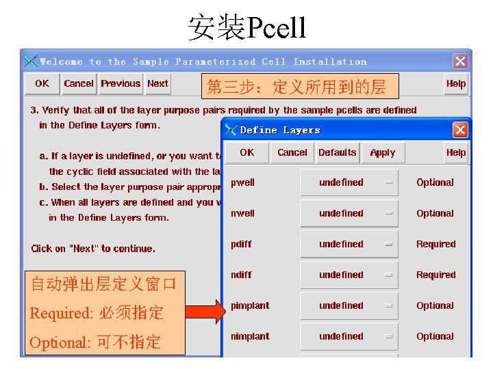
输入以下内容: set. Skill. Path(cons(prepend. Install. Path(“samples/ ROD/rod. Pcells”) get. Skill. Path())) load(“install/spc. Load.")


 >cd.")


![查看lvs command file *description … model … 针对晶体管 = mos[n], n mos[p], p bjt[pv],](https://slidetodoc.com/presentation_image_h/c06c37a25c83d4ac74773bed3183029c/image-62.jpg "查看lvs command file *description … model … 针对晶体管 = mos[n], n mos[p], p bjt[pv],")
![修改lvs command file *description 针对晶体管 … model = mos[nm], n mos[pm], p bjt[pv], q](https://slidetodoc.com/presentation_image_h/c06c37a25c83d4ac74773bed3183029c/image-63.jpg "修改lvs command file *description 针对晶体管 … model = mos[nm], n mos[pm], p bjt[pv], q")
![查看lvs command file 针对电阻 *description … model … = mos[n], n mos[p], p bjt[pv],](https://slidetodoc.com/presentation_image_h/c06c37a25c83d4ac74773bed3183029c/image-64.jpg "查看lvs command file 针对电阻 *description … model … = mos[n], n mos[p], p bjt[pv],")


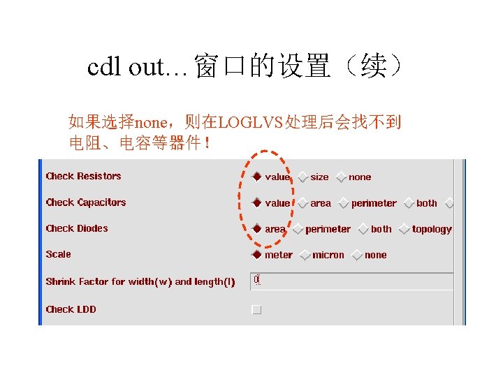


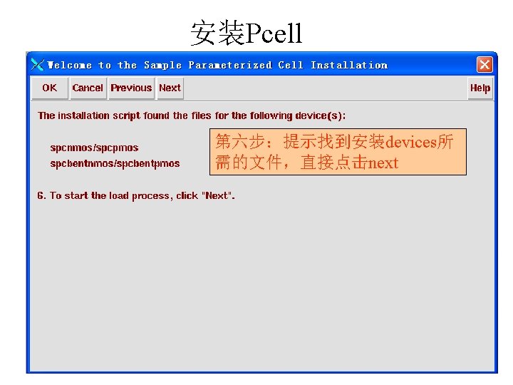
 – 进检查目录 • cd ~/project/verify – 用PDRACULA编译command file • PDRACULA •")
 SUMMARY REPORT ******* … ******* STATISTICS AFTER REDUCE")


- Slides: 79
第六讲 Virtuoso Layout Editor LVS verification 李福乐 lifule@tsinghua. edu. cn
Contacts + + = poly 1 contact metal 1 + via p 1到m 1的连接 = metal 2 m 1到m 2的连接
Contacts
Contacts => p 2 co + poly 1 contact metal 1 => m 1 m 2 + metal 1 => nsdco psdco + + via + metal 2 + active contact metal 1
Contacts Dot pin indicating connectivity via. Layer via. Purpose layer 2 purpose 2 layer 1 purpose 1 enc. By. Layer 2
Contacts
Contacts sym. Contact. Device( ; (name via. Layer via. Purpose layer 1 purpose 1 layer 2 purpose 2 ; w l (row column x. Pitch y. Pitch x. Bias y. Bias) enc. By. Layer 1 ; enc. By. Layer 2 legal. Region) (m 1 m 2 via 1 drawing metal 2 drawing 0. 7 (1 1 1. 5 center) 0. 4 _NA_) (nsdco contact drawing metal 1 drawing active drawing 0. 6 (1 1 1. 2 center) 0. 4 _NA_) (p 2 co contact drawing metal 1 drawing poly 1 drawing 0. 6 (1 1 1. 2 center) 0. 4 _NA_) )
Contacts 例子:修改p 2 co,将m 1对co改为最小包围 sym. Contact. Device( ; (name via. Layer via. Purpose layer 1 purpose 1 layer 2 purpose 2 ; w l (row column x. Pitch y. Pitch x. Bias y. Bias) enc. By. Layer 1 ; enc. By. Layer 2 legal. Region) 0. 4 => 0. 3 (p 2 co contact drawing metal 1 drawing poly 1 drawing 0. 6 (1 1 1. 2 center) 0. 3 0. 4 _NA_) )
最后 ok Contacts
Contacts 按o键,create contact 生成contact array (5 x 5) m 1+ m 2
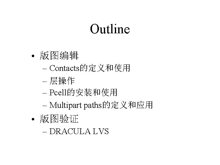
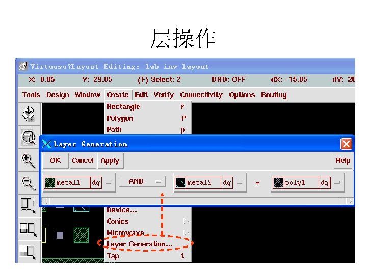
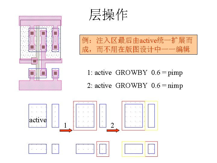
层操作 1 1: metal 1 AND metal 2 = poly 1 2: metal 1 ANDNOT metal 2 = poly 1 3: metal 1 OR metal 2 = poly 1 4: metal 1 XOR metal 2 = poly 1 5: metal 1 GROWBY 0. 4 = poly 1 方法:先选中要操作的层,然后 点击create – layer generation… 2 m 1 3 4 5 p 1
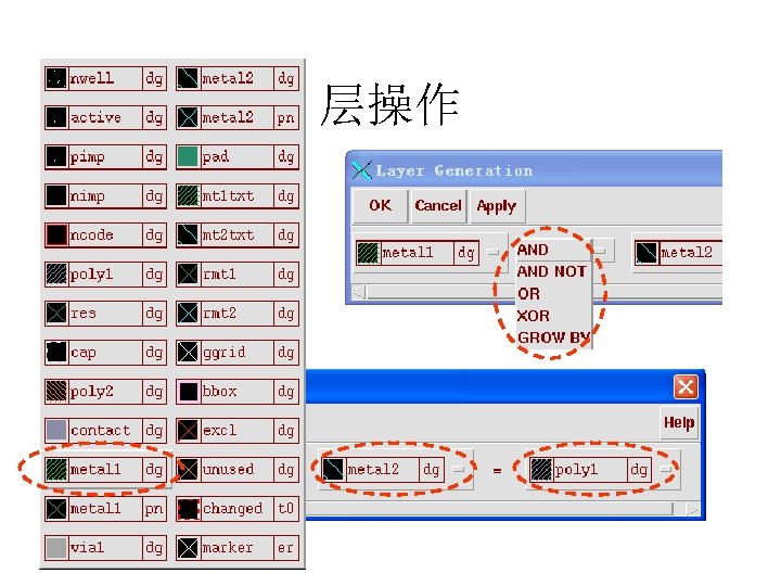
层操作 1 2 1: contact GROWBY 0. 4 = poly 1 2: contact GROWBY 0. 3 = metal 1
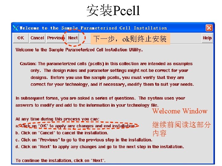
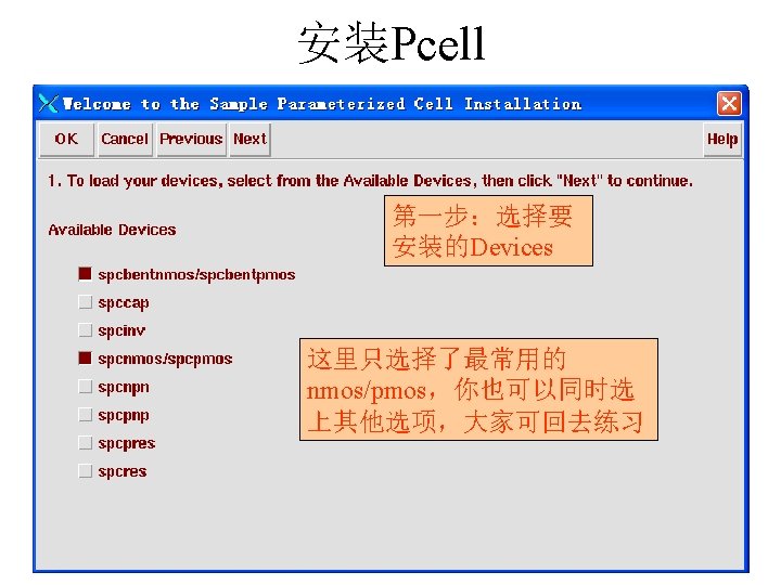
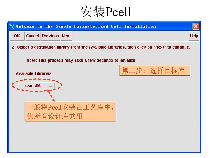
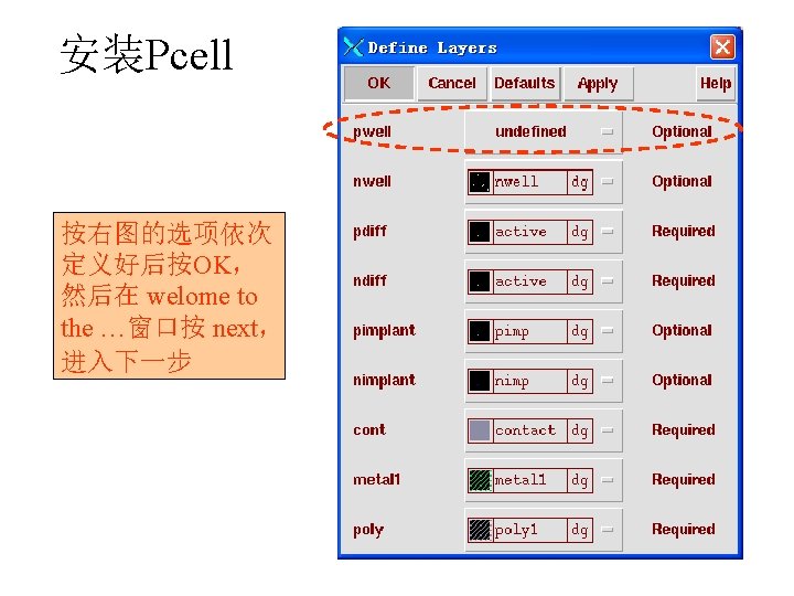
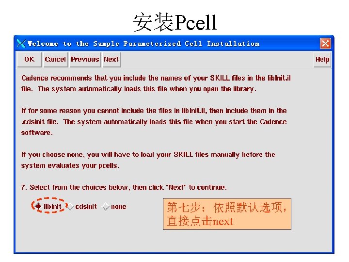
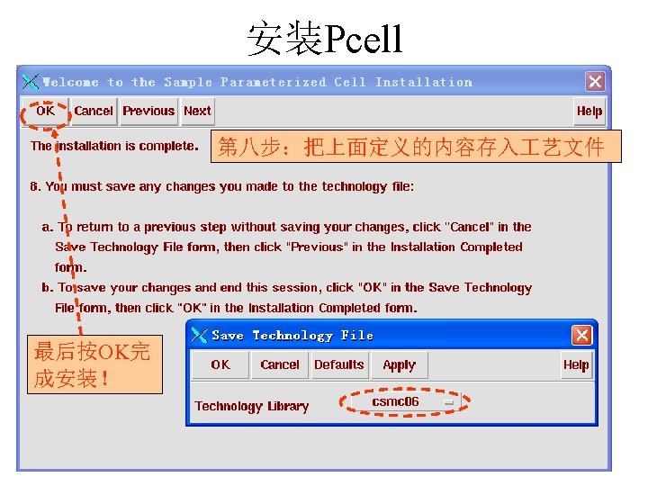
安装Pcell 在CIW(命令注释窗口)输入以下内容: set. Skill. Path(cons(prepend. Install. Path(“samples/ ROD/rod. Pcells”) get. Skill. Path())) load(“install/spc. Load. Install. il”) spc. Install() 注意大小写不要弄错! 快捷方法:选中并 ctrl+c,然后在CIW中点 击中键,就可以把复制的内容粘贴过去,最 后回车
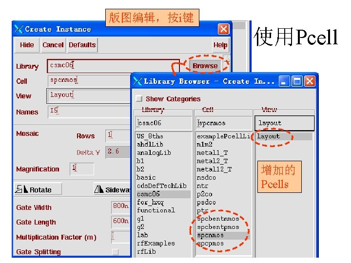
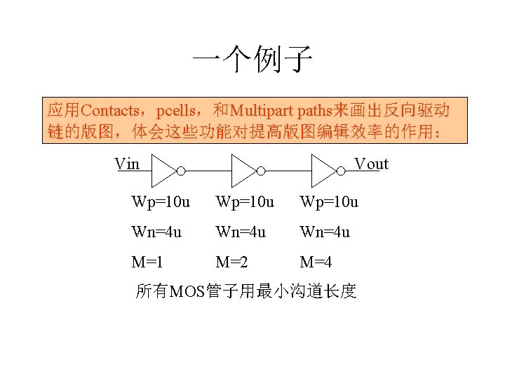
使用Pcell 利用Pcell生成 W=5 u; L=0. 6 u M=2 的PMOS管
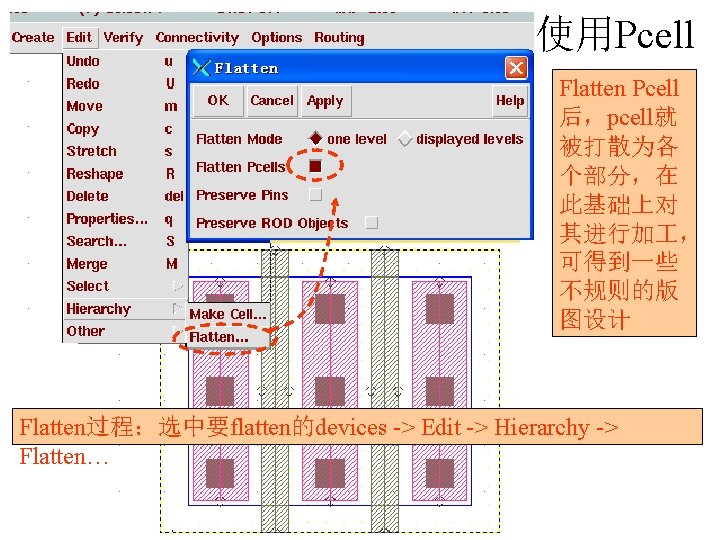
例: Flatten & adjust
Multipart paths的定义和应用
Multipart paths metal 1 Master path pimp active contact Sub paths Guardring 定义Multipart paths的目的在于提高版图编辑效率: 1. 一次性拉出符合设计规则的多个图形; 2. 调整master path, sub paths自动随之调整
Multipart paths Master path 按F 3
Multipart paths Subparts: *offset subpaths *enclosure subpaths *sets of subrectangle
Multipart paths
Multipart paths
Multipart paths
Multipart paths
Multipart paths Template里 增加了 pguradring
Multipart paths Name: pguardring 改为 nguardring 在pguardring的基础上 修改生成nguardring
Multipart paths 删去subpath: pimp,添加 subpath: nimp
Multipart paths 将nguardring的定义存入 艺文件
Multipart paths Template里 增加了 nguradring
Multipart paths • 除了定义guardring以外,multipart paths 还常用于定义以下结构: – Busses – Contact arrays – transistors
Multipart paths Sub parts Master path
Multipart paths Subpaths Master path 调整master path, subpaths自动随之一起调整
版图验证 DRACULA LVS
Full-custom verification flow Layout Dracula Command Files Dracula DRC ERC LVS LPE Netlist stream out GDS II Postlayout Simulation Hspice Tape Out 这里主要指晶体管级设计, 后仿真采用Spice 具 Schematic Netlist Text & graphic error reports
Flow of running Dracula Command File Errors Layout Stream Out GDS II Database PDRACULA Command File Processor jxrun. com / jxrun. sub Run File Dracula Program Schematic CDL Out CDL Netlist LOGLVS LVSLOGIC. DAT for LVS, LPE Text & Graphic error reports
Command File Dracula是按批处理方式 作的验证 具,其执行 的一系列命令都在命令文件中,文件结构为: Command files Heading Description Block Define database name, format, I/O information… Input Layer Block Define input layer number text sequence, connection Operation Block Define layer operation verification type…
修改 DRC Command File *description system primary indisk outdisk scale resolution printfile … = gds 2 = drclvs. gds = drclvs. out = 0. 001 mic = 0. 05 mic = drcpr 定义Dracula使用Gds. II格式 Cell名和对应的stream out后的 gdsii文件名,为了避免经常修 改,最好固定为一个名字,对 每个cell进行验证,都先save as为这个名字的cell 输出的error gdsii
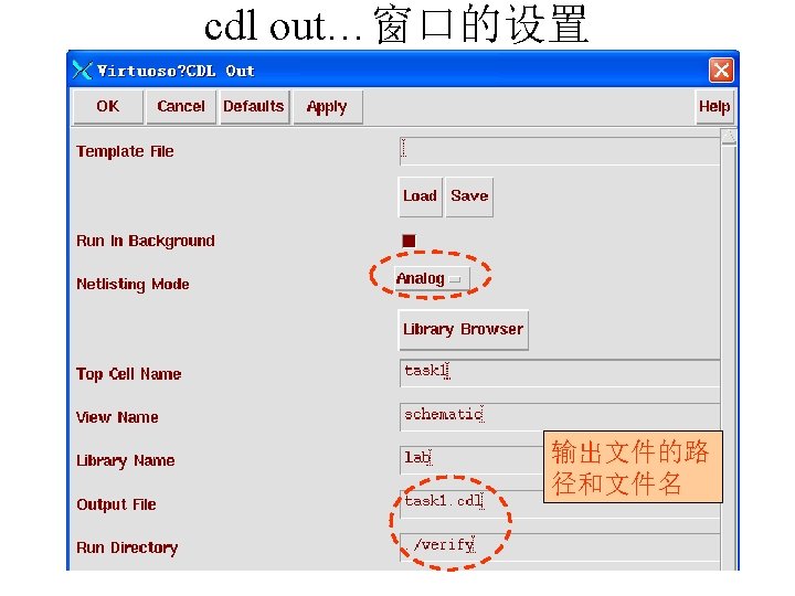
DRC Verification 取得DRC Command file 一般为 艺厂商提供 修改DRC Command file Stream out (GDSII) >cd. /verify >PDRACULA 见第三讲课件 : /g drc : /f >jxrun. com Tool -> Dracula interactive… Command file 文件名
修改 LVS Command File *description system primary indisk outdisk scale resolution printfile mode schematic … 定义Dracula使用Gds. II格式 = gds 2 Cell名和对应的stream out后的 = drclvs gdsii文件名,为了避免经常修 = drclvs. gds 改,最好固定为一个名字,对 = drclvs. out 每个cell进行验证,都先save = 0. 001 mic as为这个名字的cell = 0. 05 mic = lvspr 扩展名为lvs, = exec now 即lvspr. lvs为 = LVSLOGIC. DAT Text error reports LOGLVS处理后的网表
LVS Verification 取得LVS Command file 修改LVS Command file Layout Stream Out GDS II Database >cd. /verify >PDRACULA : /g lvs Schematic CDL Out CDL Netlist LOGLVS LVSLOGIC. DAT : /f >jxrun. com 查看lvspr. lvs Cdl out的网表,Stream out的gdsii file,Command file等 最好都放在一个专用目录下,如~/project/verify
LVS的例子 以第三讲中的第一个版图设计作业为例 lab: task 1: layout lab: task 1: schematic Layout vs. Schematic
Layout上加pin和label • Creat -> pin… • Creat -> Label… • 注意:metal 1上的pin和label要用mt 1 txt层; metal 2上的pin和label要用mt 2 txt层
查看lvs command file *description … model … 针对晶体管 = mos[n], n mos[p], p bjt[pv], q dio[np], d = res[nw], r res[pd], r res[nd], r res[p 1], r res[p 2], r = res[m 1], r res[m 2], r res[m 3], r = cap[pp], c cap[ng], c cap[mm], c 表示nmos的模型名为n,pmos的模型名为p;而 cdl out后,nmos, pmos的模型名分别为nm和pm
修改lvs command file *description 针对晶体管 … model = mos[nm], n mos[pm], p bjt[pv], q dio[np], d model = res[nw], r res[pd], r res[nd], r res[p 1], r res[p 2], r model = res[m 1], r res[m 2], r res[m 3], r model = cap[pp], c cap[ng], c cap[mm], c … ; define active devices(mos/bipolar transistors, diodes) element mos[nm] ngate py 1 nsd psub ; nmos transistor element mos[pm] pgate py 1 psd nwl ; pmos transistor … n -> nm p -> pm
查看lvs command file 针对电阻 *description … model … = mos[n], n mos[p], p bjt[pv], q dio[np], d = res[nw], r res[pd], r res[nd], r res[p 1], r res[p 2], r = res[m 1], r res[m 2], r res[m 3], r = cap[pp], c cap[ng], c cap[mm], c 电阻有很多种,模型名各不相同 注意:cdl out的网表里电阻的模 型名为rp
查看lvs command file *description … 针对电阻 *input-layer … res = 62 ; high ohm resistor protection area … *operation 定义了高阻层,却没有高阻电阻的定义! … ; definition of resistor id layers and nwell rnwl nwlres ; nwell resistor and ncomp rpycmp ndres ; ncomp resistor and pcomp rpycmp pdres ; pcomp resistor and poly 1 rpycmp py 1 res ; poly 1 resistor and poly 2 rpycmp py 2 res ; poly 2 resistor and metal 1 rmt 1 res; metal 1 resistor and metal 2 rmt 2 res; metal 2 resistor …
修改lvs command file … 针对电阻 *operation … rpycmp -> res,将poly 2 resistor定义为高阻电阻 ; definition of resistor id layers and nwell rnwl nwlres ; nwell resistor and ncomp rpycmp ndres ; ncomp resistor and pcomp rpycmp pdres ; pcomp resistor and poly 1 rpycmp py 1 res ; poly 1 resistor and poly 2 res py 2 res ; poly 2 resistor and metal 1 rmt 1 res; metal 1 resistor and metal 2 rmt 2 res; metal 2 resistor … 原来为 6. 0,这里改 ; define passive devices(resistors, capacitors) 为高阻的方块电阻 … element res[p 2] py 2 res py 2 ; poly 2 resistor parameter res[p 2]996 …
执行LOGLVS • 在verify目录下,启动LOGLVS – cd ~/project/verify – LOGLVS • 回车后,屏幕上会提示command summary,我们 用到的主要是cir filename, con cellname, summary, exit • 在屏幕提示ENTER COMMAND后,输入: – – cir task 1. cdl 执行这些命令后,得到LVSLOGIC. DAT con task 1 sum 即summary,用于报告网表中的元件种类个个数 x 即exit
Stream out GDSII • 导出GDSII文件 – 在layout editor窗口,将编辑的版图另存为 lab : drclvs : layout – 导出 GDSII文件 • CIW窗口,点击File Export stream…弹出 stream out 窗口 • 点击 library browser,选择 lab : drclvs : layout • 在 Output File 中填写目录. /verify • OK
执行LVS验证 • Dracula设计规则检查(LVS) – 进检查目录 • cd ~/project/verify – 用PDRACULA编译command file • PDRACULA • /get lvs 或简单地 /g lvs • /finish 或简单地 /f – 执行上一步生成的rule file • jxrun. com 执行完后得到报告文件:lvspr. lvs
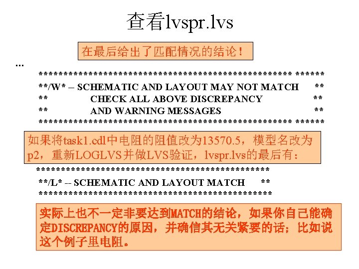
查看lvspr. lvs … ******* REDUCE (LAYOUT) SUMMARY REPORT ******* … ******* STATISTICS AFTER REDUCE **** MOS BJT RES INV DIODE CAP SDWI PDWI SUPI 1 0 0 0 0 … ******* REDUCE (SCHEMATIC) SUMMARY REPORT***** … ******* STATISTICS AFTER REDUCE **** MOS BJT RES INV DIODE CAP SDWI PDWI SUPI 1 0 0 0 0 … 这两部分分别给出shematic和layout中元件的类 型和数量,两部分必须完全一致!
… 1 查看lvspr. lvs ************************** CORRESPONDENCE NODE PAIRS ****************************** 这部分给出相互对应的I/O,layout所标的pin和label应 全部被DRACULA抓读,并与shematic一一对应! SCHEMATICS LAYOUT PAD TYPE GND! 1 GND VDD! 2 VDD IN 3 IN OUT 4 OUT ***TOTAL = 4*** 1 7 4 2 G P I O (Ground (Power pad) (Input pad) (Output pad) NUMBER OF VALID CORRESPONDENCE NODE PAIRS = 2
… 1 查看lvspr. lvs ************************** LVS DEVICE MATCH SUMMARY ****************************** 这部分给出元件匹配情况,un-matched的元件必须为 0! NUMBER OF UN-MATCHED SCHEMATICS DEVICES NUMBER OF UN-MATCHED LAYOUT DEVICES NUMBER OF MATCHED SCHEMATICS DEVICES NUMBER OF MATCHED LAYOUT DEVICES = = 0 0 2 2 … ************************** DEVICE MATCHING SUMMARY BY TYPE ****************************** 这部分考虑了元件subtype,电阻模型名不匹配! TYPE SUB-TYPE MOS RES NM RP P 2 TOTAL DEVICE SCH. LAY. 1 1 1 0 0 1 UN-MATCHED DEVICE SCH. LAY. 0 0 0
… 1 查看lvspr. lvs ************************** DISCREPANCY POINTS LISTING ******************************* 这部分给出了不匹配的情况, 电阻模型名和阻值不匹配! ************ DISCREPANCY 1 *********** DEV 2 RES RP ---- OUT, VDD! SUB-TYPE = RP VALUE=15000. 0 TOTAL RR 0 : DEV 6 RES P 2 : X=-35. 60 Y=9. 70 OUT, VDD! SUB-TYPE = P 2 VALUE=13570. 5 1 DISCREPANCY POINTS REPORTED