Trends in the Infrastructure of Computing CSCE 190
- Slides: 42
Trends in the Infrastructure of Computing CSCE 190: Computing in the Modern World Jason D. Bakos Heterogeneous and Reconfigurable Computing Group
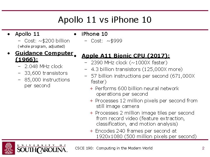
Apollo 11 vs i. Phone 10 • Apollo 11 – Cost: ~$200 billion • i. Phone 10 – Cost: ~$999 (whole program, adjusted) • Guidance Computer • Apple A 11 Bionic CPU (2017): (1966): – 2. 048 MHz clock – 33, 600 transistors – 85, 000 instructions per second – 2390 MHz clock (~1000 X faster) – 4. 3 billion transistors (125, 000 X more) – 57 billion instructions per second (671, 000 X faster) + Performs 600 billion neural network operations per second + Processes 12 million pixels per second from still image camera + Processes 2 million image tiles per second from record video (feature extraction, classification, and motion analysis) + Encodes 240 frames per second at 1920 x 1080 (500 million pixels per second) CSCE 190: Computing in the Modern World 2
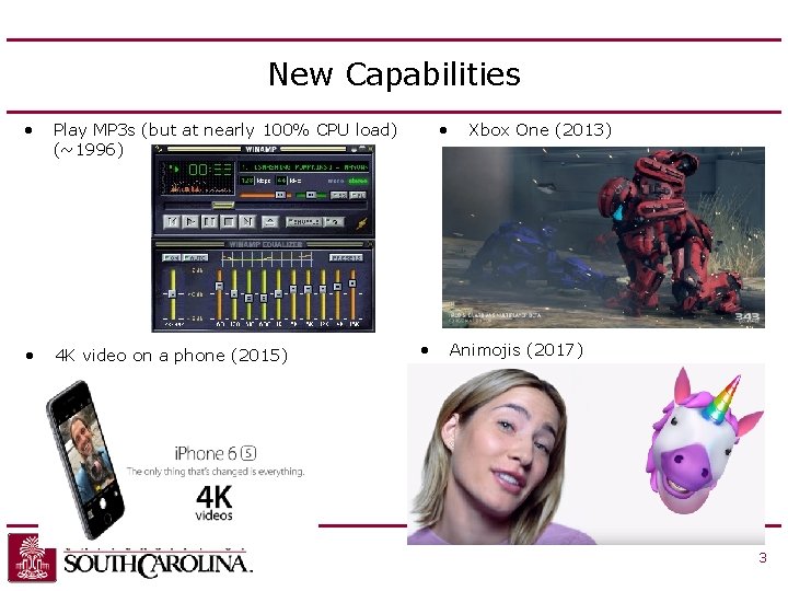
New Capabilities • Play MP 3 s (but at nearly 100% CPU load) (~1996) • 4 K video on a phone (2015) • • Xbox One (2013) Animojis (2017) 3
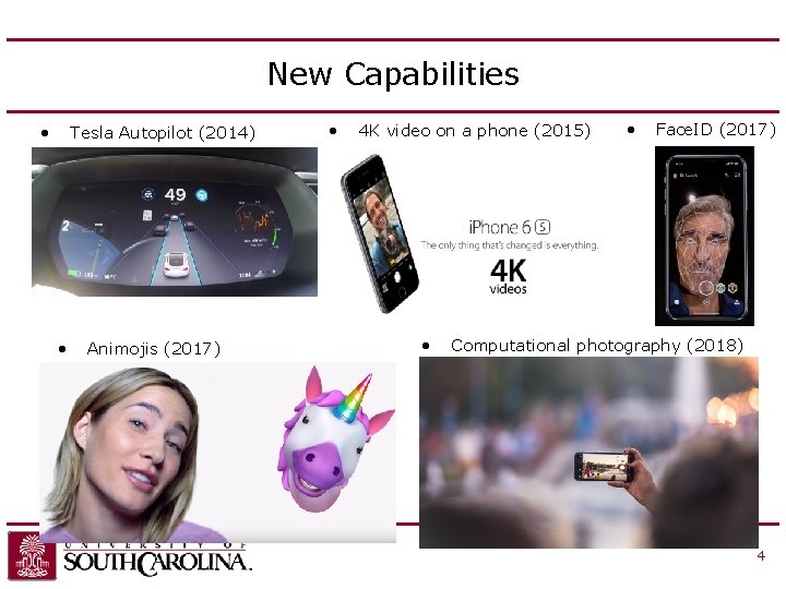
New Capabilities • Tesla Autopilot (2014) • Animojis (2017) • 4 K video on a phone (2015) • • Face. ID (2017) Computational photography (2018) 4
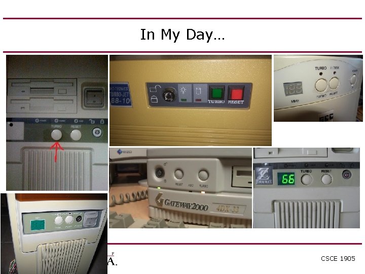
In My Day… CSCE 1905
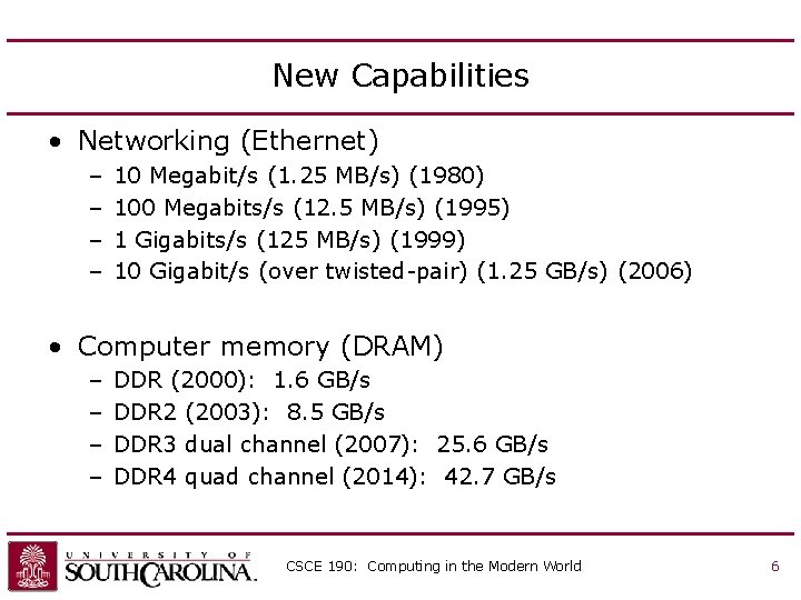
New Capabilities • Networking (Ethernet) – – 10 Megabit/s (1. 25 MB/s) (1980) 100 Megabits/s (12. 5 MB/s) (1995) 1 Gigabits/s (125 MB/s) (1999) 10 Gigabit/s (over twisted-pair) (1. 25 GB/s) (2006) • Computer memory (DRAM) – – DDR (2000): 1. 6 GB/s DDR 2 (2003): 8. 5 GB/s DDR 3 dual channel (2007): 25. 6 GB/s DDR 4 quad channel (2014): 42. 7 GB/s CSCE 190: Computing in the Modern World 6
i. Clicker • Answer the following multiple-choice question. • I belong to the student chapter of a professional organization in Computing – A. ACM – B. IEEE or IEEE Computer Society or both – C. Neither UNIVERSITY OF SOUTH CAROLINA Department of Computer Science and Engineering
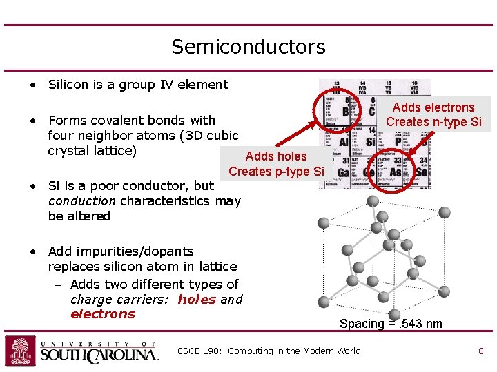
Semiconductors • Silicon is a group IV element Adds electrons Creates n-type Si • Forms covalent bonds with four neighbor atoms (3 D cubic crystal lattice) Adds holes Creates p-type Si • Si is a poor conductor, but conduction characteristics may be altered • Add impurities/dopants replaces silicon atom in lattice – Adds two different types of charge carriers: holes and electrons Spacing =. 543 nm CSCE 190: Computing in the Modern World 8
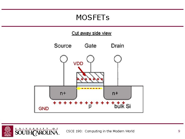
MOSFETs Cut away side view VDD +++++++ ------- GND +++++++ CSCE 190: Computing in the Modern World 9
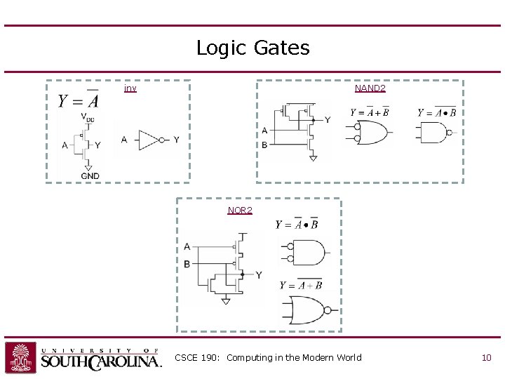
Logic Gates inv NAND 2 NOR 2 CSCE 190: Computing in the Modern World 10
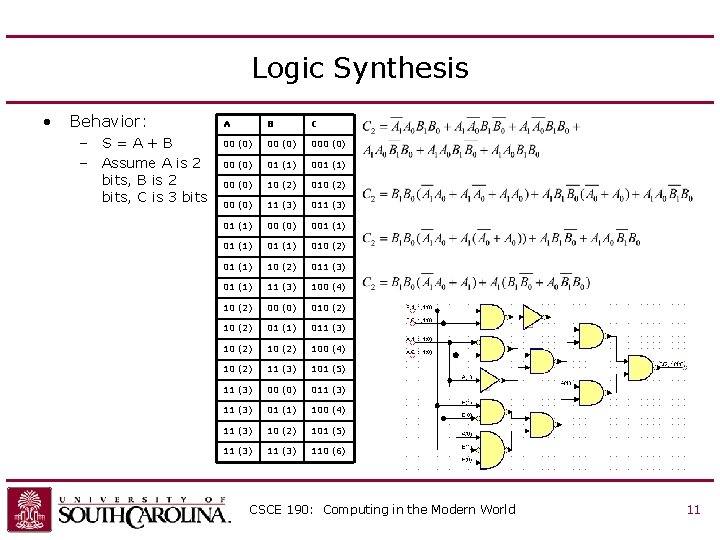
Logic Synthesis • Behavior: – S=A+B – Assume A is 2 bits, B is 2 bits, C is 3 bits A B C 00 (0) 000 (0) 01 (1) 00 (0) 10 (2) 00 (0) 11 (3) 01 (1) 00 (0) 001 (1) 010 (2) 01 (1) 10 (2) 011 (3) 01 (1) 11 (3) 100 (4) 10 (2) 00 (0) 010 (2) 01 (1) 011 (3) 10 (2) 100 (4) 10 (2) 11 (3) 101 (5) 11 (3) 00 (0) 011 (3) 01 (1) 100 (4) 11 (3) 10 (2) 101 (5) 11 (3) 110 (6) CSCE 190: Computing in the Modern World 11
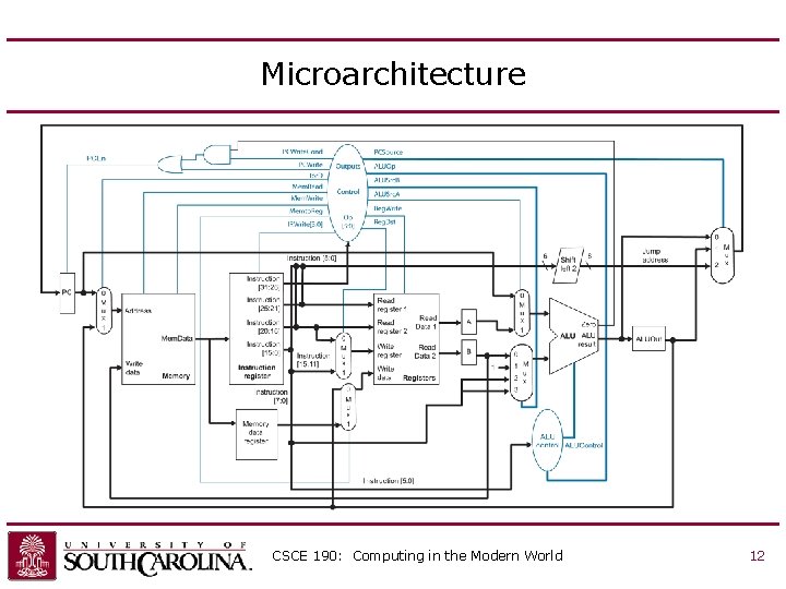
Microarchitecture CSCE 190: Computing in the Modern World 12
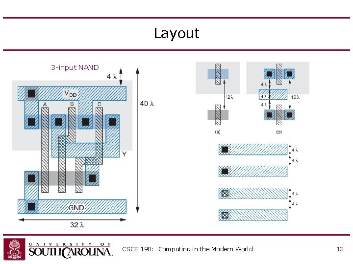
Layout 3 -input NAND CSCE 190: Computing in the Modern World 13
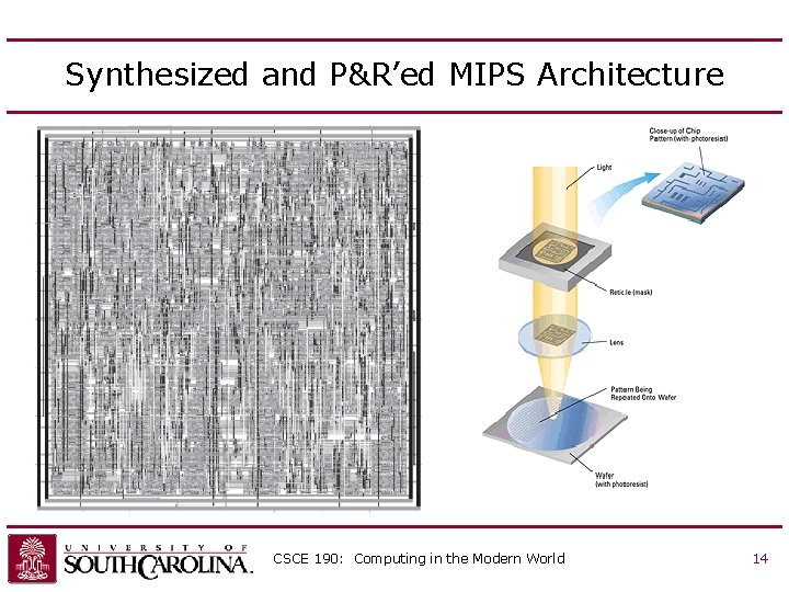
Synthesized and P&R’ed MIPS Architecture CSCE 190: Computing in the Modern World 14
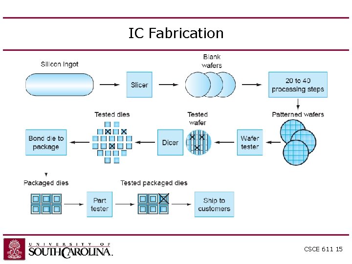
IC Fabrication CSCE 611 15
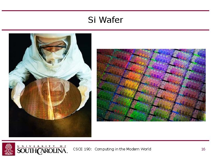
Si Wafer CSCE 190: Computing in the Modern World 16
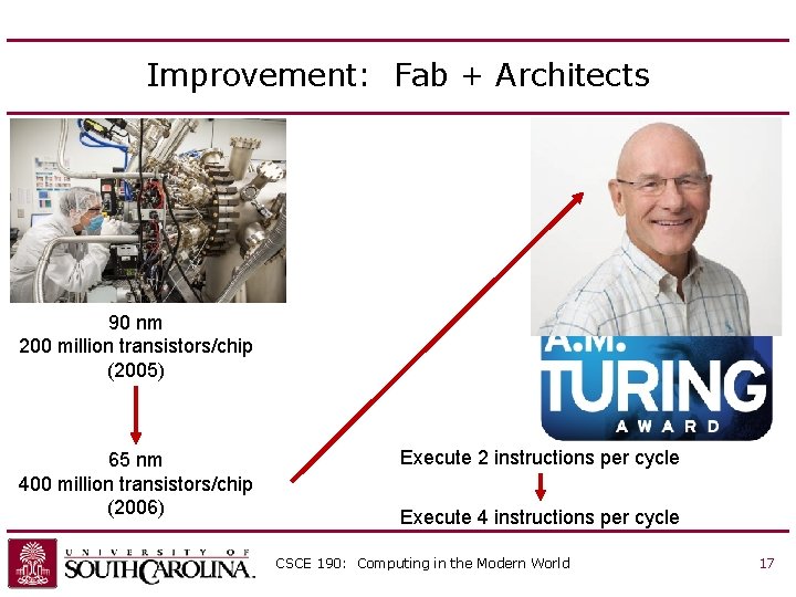
Improvement: Fab + Architects 90 nm 200 million transistors/chip (2005) 65 nm 400 million transistors/chip (2006) Execute 2 instructions per cycle Execute 4 instructions per cycle CSCE 190: Computing in the Modern World 17
i. Clicker • Answer the following multiple-choice question. • The A. M. Turing Award – A. is named after Alan M. Turing (1912 1954) – B. is sometimes called “the Nobel Prize of Computing” – C. entitles its recipient to a USD 1 million award financed by Google – D. was first awarded in 1966 – E. all the above UNIVERSITY OF SOUTH CAROLINA Department of Computer Science and Engineering
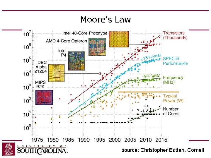
Moore’s Law source: Christopher Batten, Cornell
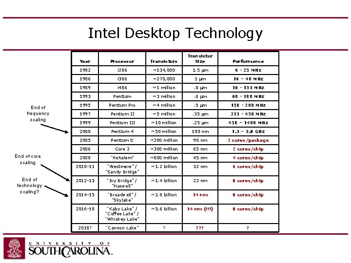
Intel Desktop Technology End of frequency scaling End of core scaling End of technology scaling? Year Processor Transistors Transistor Size Performance 1982 i 286 ~134, 000 1. 5 mm 6 - 25 MHz 1986 i 386 ~270, 000 1 mm 16 – 40 MHz 1989 i 486 ~1 million . 8 mm 16 - 133 MHz 1993 Pentium ~3 million . 6 mm 60 - 300 MHz 1995 Pentium Pro ~4 million . 5 mm 150 - 200 MHz 1997 Pentium II ~5 million . 35 mm 233 - 450 MHz 1999 Pentium III ~10 million . 25 mm 450 – 1400 MHz 2000 Pentium 4 ~50 million 180 nm 1. 3 – 3. 8 GHz 2005 Pentium D ~200 million 90 nm 2 cores/package 2006 Core 2 ~300 million 65 nm 2 cores/chip 2008 “Nehalem” ~800 million 45 nm 4 cores/chip 2010 -11 “Westmere” / “Sandy Bridge” ~1. 2 billion 32 nm 6 cores/chip 2012 -13 “Ivy Bridge” / ”Haswell” ~1. 4 billion 22 nm 8 cores/chip 2014 -15 “Broadwell” / ”Skylake” ~2. 8 billion 14 nm 8 cores/chip 2016 -18 “Kaby Lake” / “Coffee Lake” / “Whiskey Lake” ~5. 6 billion 14 nm (!!!) 8 cores/chip 2018? “Cannon Lake” ? ? ? ? ?
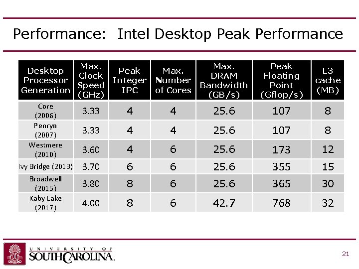
Performance: Intel Desktop Peak Performance Max. Desktop Clock Processor Speed Generation (GHz) Core 3. 33 (2006) Penryn 3. 33 (2007) Westmere 3. 60 (2010) Peak Integer IPC Max. Number of Cores Max. DRAM Bandwidth (GB/s) Peak Floating Point (Gflop/s) L 3 cache (MB) 4 4 25. 6 107 8 4 6 25. 6 12 32 Ivy Bridge (2013) 3. 70 6 6 25. 6 Broadwell (2015) Kaby Lake (2017) 3. 80 8 6 25. 6 173 355 365 4. 00 8 6 42. 7 768 15 30 21
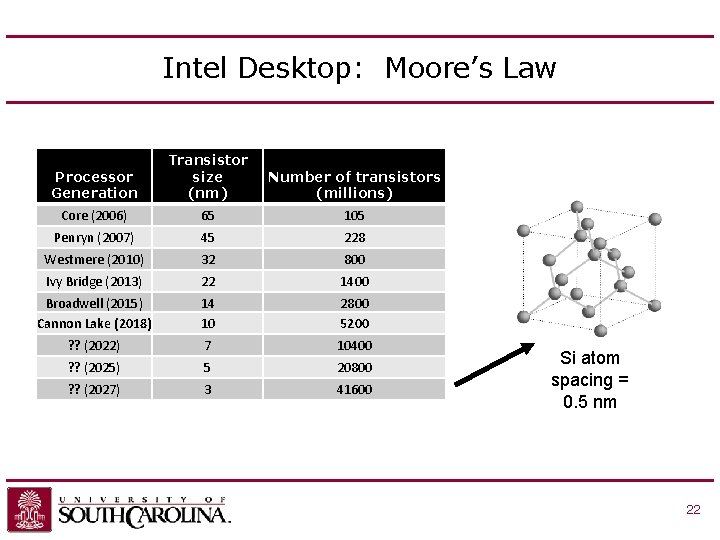
Intel Desktop: Moore’s Law Processor Generation Transistor size (nm) Number of transistors (millions) Core (2006) 65 105 Penryn (2007) 45 228 Westmere (2010) 32 800 Ivy Bridge (2013) 22 1400 Broadwell (2015) Cannon Lake (2018) 14 10 2800 5200 ? ? (2022) 7 10400 ? ? (2025) 5 20800 ? ? (2027) 3 41600 Si atom spacing = 0. 5 nm 22
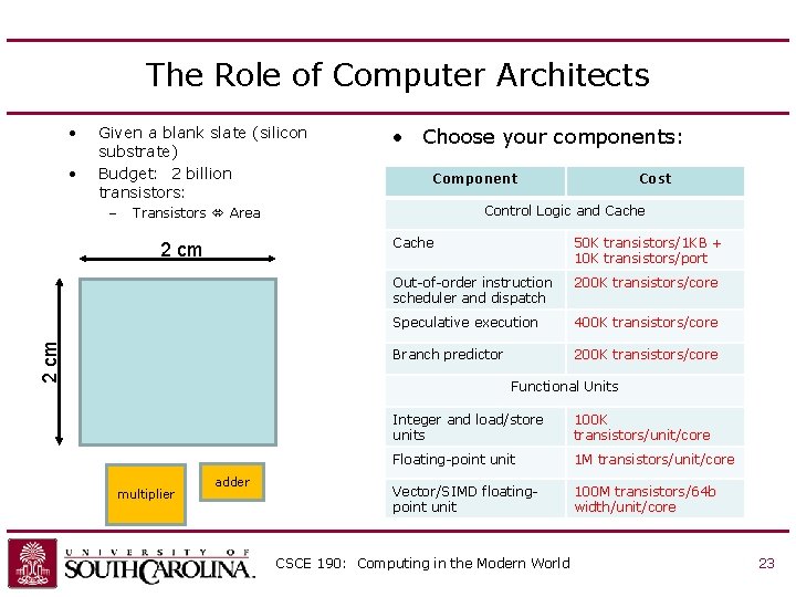
The Role of Computer Architects • • Given a blank slate (silicon substrate) Budget: 2 billion transistors: – • Choose your components: Component Control Logic and Cache Transistors Area 2 cm Cost Cache 50 K transistors/1 KB + 10 K transistors/port Out-of-order instruction scheduler and dispatch 200 K transistors/core Speculative execution 400 K transistors/core Branch predictor 200 K transistors/core Functional Units multiplier adder Integer and load/store units 100 K transistors/unit/core Floating-point unit 1 M transistors/unit/core Vector/SIMD floatingpoint unit 100 M transistors/64 b width/unit/core CSCE 190: Computing in the Modern World 23
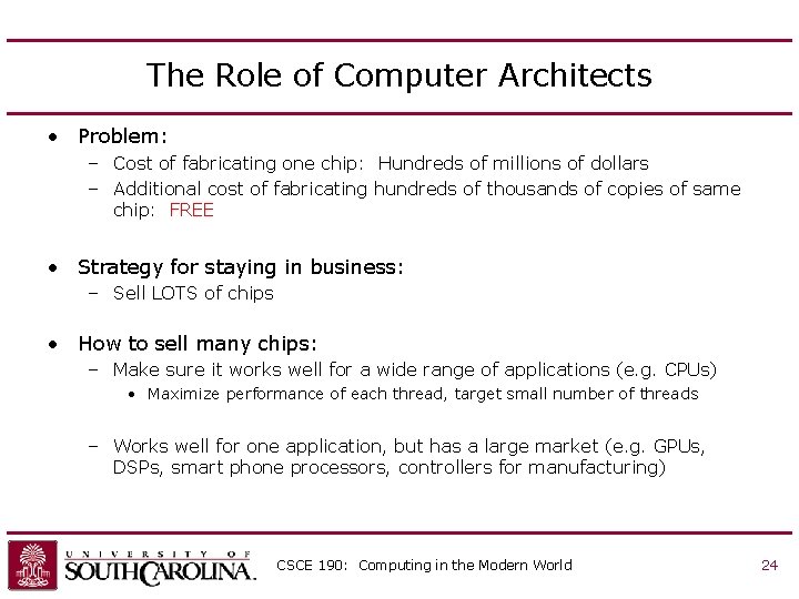
The Role of Computer Architects • Problem: – Cost of fabricating one chip: Hundreds of millions of dollars – Additional cost of fabricating hundreds of thousands of copies of same chip: FREE • Strategy for staying in business: – Sell LOTS of chips • How to sell many chips: – Make sure it works well for a wide range of applications (e. g. CPUs) • Maximize performance of each thread, target small number of threads – Works well for one application, but has a large market (e. g. GPUs, DSPs, smart phone processors, controllers for manufacturing) CSCE 190: Computing in the Modern World 24
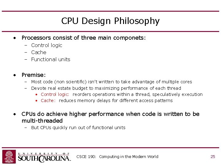
CPU Design Philosophy • Processors consist of three main componets: – Control logic – Cache – Functional units • Premise: – Most code (non scientific) isn’t written to take advantage of multiple cores – Devote real estate budget to maximizing performance of each thread • Control logic: reorders operations within a thread, speculatively execution • Cache: reduces memory delays for different access patterns • CPUs do achieve higher performance when code is written to be multi-threaded – But CPUs quickly run out of functional units CSCE 190: Computing in the Modern World 25
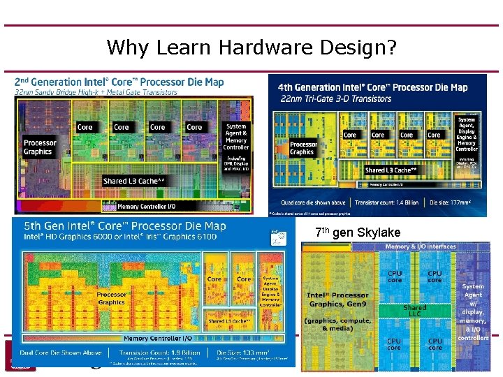
Why Learn Hardware Design? 7 th gen Skylake CSCE 611 26
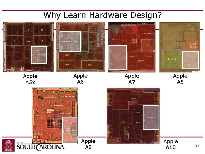
Why Learn Hardware Design? Apple A 5 x Apple A 6 Apple A 9 Apple A 7 Apple A 8 Apple A 10 27
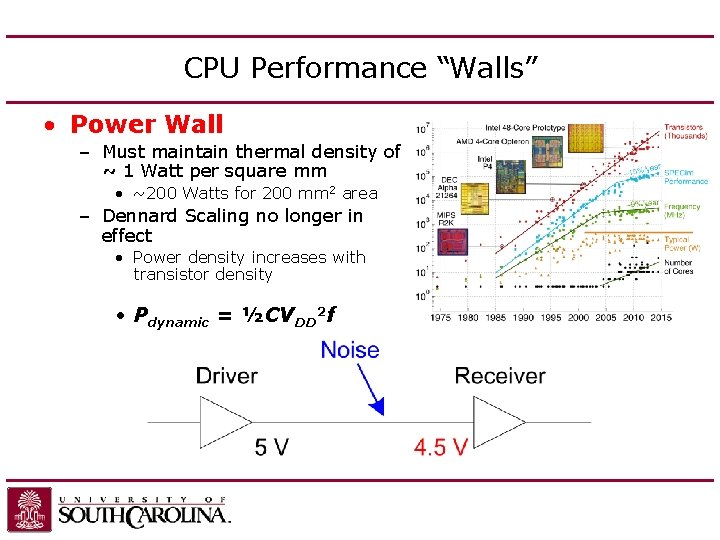
CPU Performance “Walls” • Power Wall – Must maintain thermal density of ~ 1 Watt per square mm • ~200 Watts for 200 mm 2 area – Dennard Scaling no longer in effect • Power density increases with transistor density • Pdynamic = ½CVDD 2 f
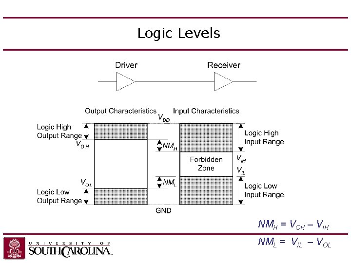
Logic Levels NMH = VOH – VIH NML = VIL – VOL
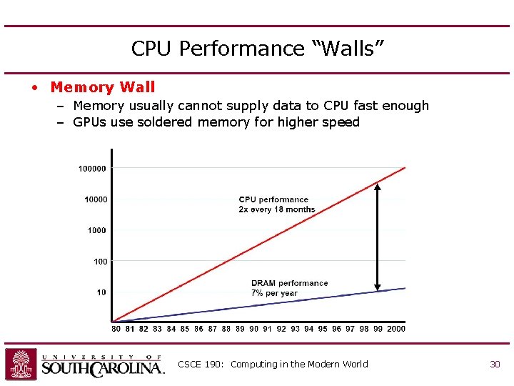
CPU Performance “Walls” • Memory Wall – Memory usually cannot supply data to CPU fast enough – GPUs use soldered memory for higher speed CSCE 190: Computing in the Modern World 30
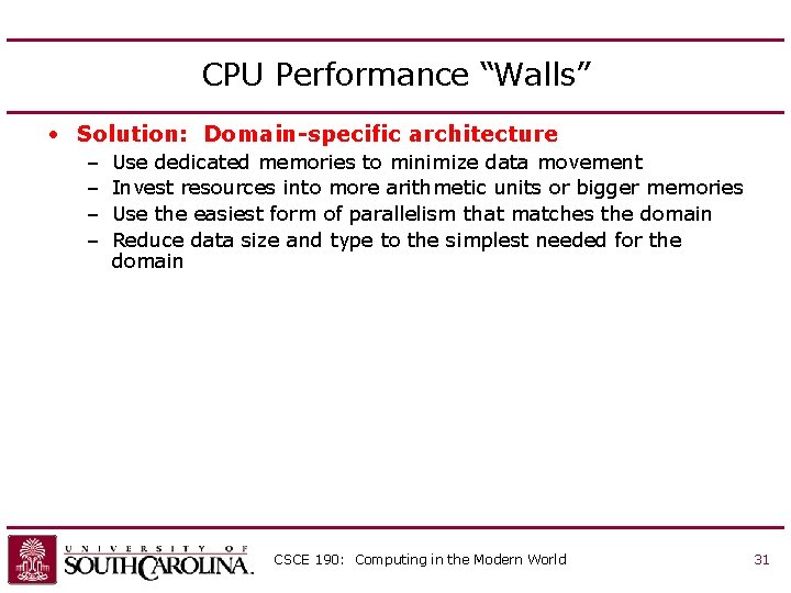
CPU Performance “Walls” • Solution: Domain-specific architecture – – Use dedicated memories to minimize data movement Invest resources into more arithmetic units or bigger memories Use the easiest form of parallelism that matches the domain Reduce data size and type to the simplest needed for the domain CSCE 190: Computing in the Modern World 31
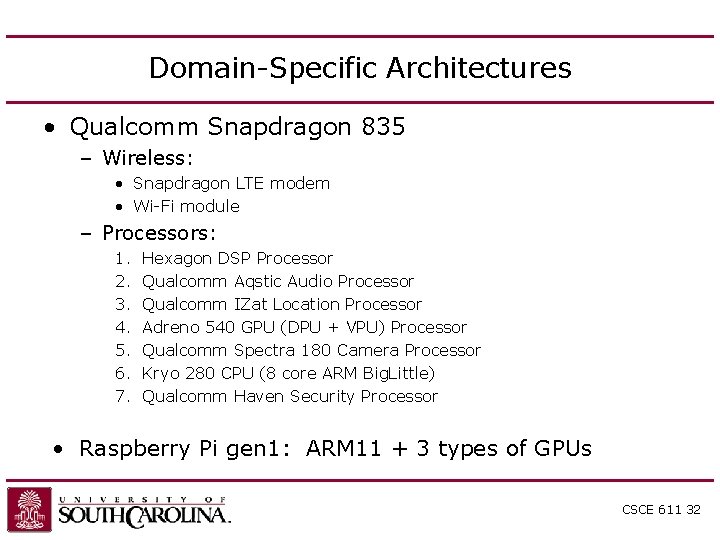
Domain-Specific Architectures • Qualcomm Snapdragon 835 – Wireless: • Snapdragon LTE modem • Wi-Fi module – Processors: 1. 2. 3. 4. 5. 6. 7. Hexagon DSP Processor Qualcomm Aqstic Audio Processor Qualcomm IZat Location Processor Adreno 540 GPU (DPU + VPU) Processor Qualcomm Spectra 180 Camera Processor Kryo 280 CPU (8 core ARM Big. Little) Qualcomm Haven Security Processor • Raspberry Pi gen 1: ARM 11 + 3 types of GPUs CSCE 611 32
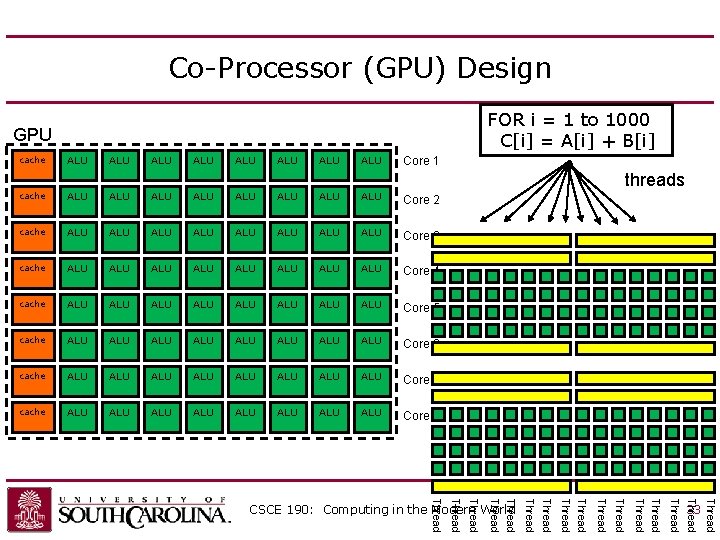
Co-Processor (GPU) Design FOR i = 1 to 1000 C[i] = A[i] + B[i] GPU cache ALU ALU Core 1 threads cache ALU ALU Core 2 cache ALU ALU Core 3 cache ALU ALU Core 4 cache ALU ALU Core 5 cache ALU ALU Core 6 cache ALU ALU Core 7 cache ALU ALU Core 8 33 Thread Thread Thread Thread CSCE 190: Computing in the Modern World
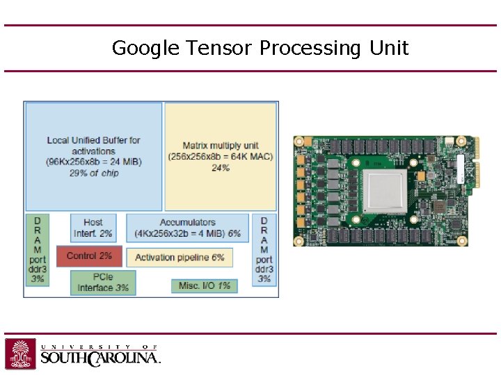
Google Tensor Processing Unit
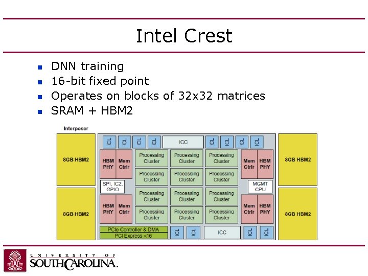
Intel Crest n n DNN training 16 -bit fixed point Operates on blocks of 32 x 32 matrices SRAM + HBM 2
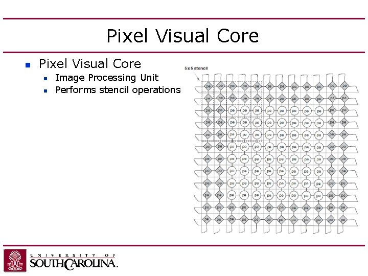
Pixel Visual Core n n Image Processing Unit Performs stencil operations
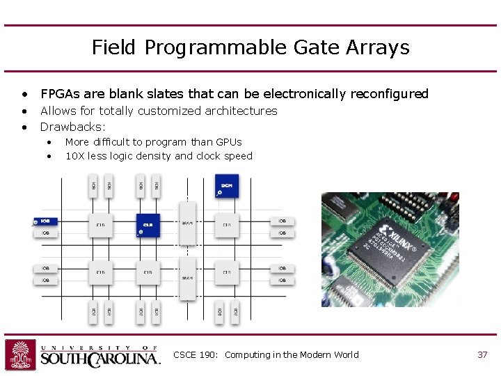
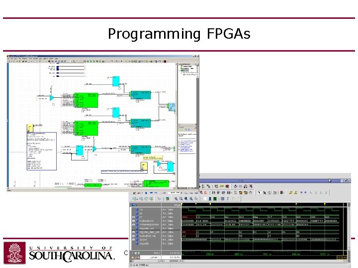
Field Programmable Gate Arrays • FPGAs are blank slates that can be electronically reconfigured • • Allows for totally customized architectures Drawbacks: • • More difficult to program than GPUs 10 X less logic density and clock speed CSCE 190: Computing in the Modern World 37
Programming FPGAs CSCE 190: Computing in the Modern World 38
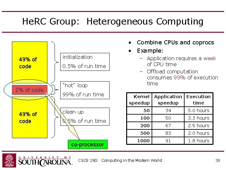
He. RC Group: Heterogeneous Computing • Combine CPUs and coprocs • Example: 49% of code 2% of code 49% of code initialization 0. 5% of run time “hot” loop 99% of run time clean up 0. 5% of run time co-processor – Application requires a week of CPU time – Offload computation consumes 99% of execution time Kernel speedup Application speedup Execution time 50 34 5. 0 hours 100 50 3. 3 hours 200 67 2. 5 hours 500 83 2. 0 hours 1000 91 1. 8 hours CSCE 190: Computing in the Modern World 39
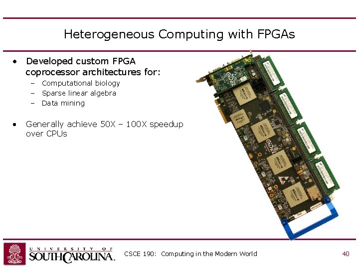
Heterogeneous Computing with FPGAs • Developed custom FPGA coprocessor architectures for: – Computational biology – Sparse linear algebra – Data mining • Generally achieve 50 X – 100 X speedup over CPUs CSCE 190: Computing in the Modern World 40
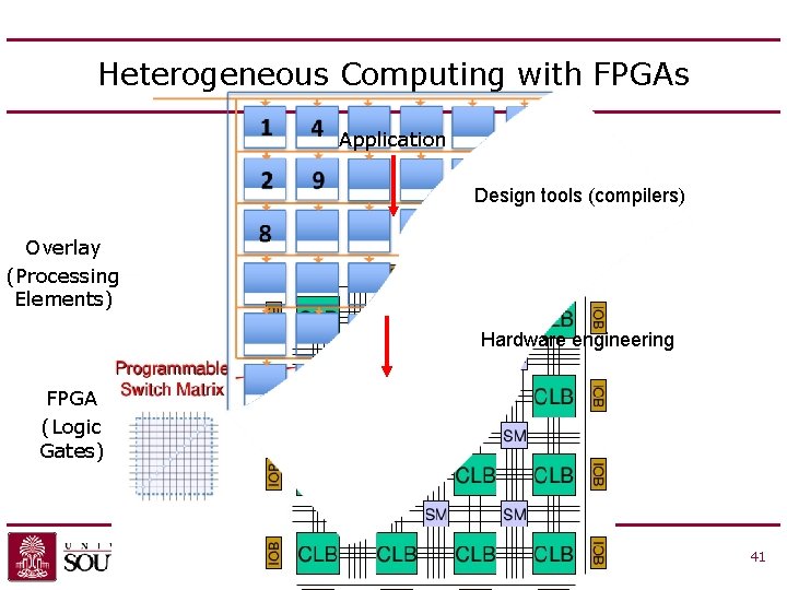
Heterogeneous Computing with FPGAs Application Design tools (compilers) Overlay (Processing Elements) Hardware engineering FPGA (Logic Gates) CSCE 190: Computing in the Modern World 41
Conclusions • Moore’s Law continues, but CPUs are benefitting from it at an increasingly lesser degree – Power Wall – Memory Wall • The future is in domain-specific architectures – Hardware designers will play increasing role in introducing new capabilities • FPGA-based computing allows for fast development of new domain specific architectures CSCE 190: Computing in the Modern World 42