Si wafer cleaning Hyeongtag Jeon Division of Materials


 Particle free 2) Metallic contaminants free 3) Organic")


 HF로")


 Element Au Pt Ag Hg Cu")

 Cu adsorption on Si wafer")
 Residual amounts for ultra-trace impurities on")


 Physical interactions 2) Physically-enhanced chemical")


 The result of oxygen removal by B. S.")


 Use of super-pure chemicals, gases")
- Slides: 39
Si wafer cleaning Hyeongtag Jeon Division of Materials Science and Engineering Hanyang University Semiconductor Materials Laboratory 1
Wafer Cleaning ◆ Objective of wafer cleaning : to remove the particulates and impurities on the silicon surface without damaging or altering the substrate surface. ◆ Importance of clean substrate surface : chemical contaminants and particulate impurities ⇒ affecting device performance, reliability and product yield of silicon circuit. Semiconductor Materials Laboratory 2
Wafer Cleaning ▶ Requirements for Si wafer cleaning process 1. Effective removal of all types of surface contaminants 2. No etching or damaging Si and Si. O 2 3. Using the contamination-free and volatilizable chemicals 4. Relatively safe, simple, and economical for production application 5. Ecologically acceptable, free of toxic waste products 6. Implementable by a variety of techniques Semiconductor Materials Laboratory 3
Wafer Contamination 1. 2. 3. 4. 5. Organics Particles Native Oxides Chemical Oxides Metallic impurities and etc Semiconductor Materials Laboratory 4
Wafer Contamination ▶ Organics → Sources : lubricants, coolants, cutting oils, fatty materials, airborne particles, detergents, organic residues → Contamination : most commonly found after evaporation of organic solvents → Effects : ① preventing effective cleaning or rinsing ② impairing good adhesion of deposited films ③ forming deleterious decomposition products during heating (ex. Si. C) Semiconductor Materials Laboratory 5
Wafer Contamination ▶ Particles → Sources : in air or liquid chemicals, adsorbed gases or vapors, factory operators, container, etc. → Contamination : most commonly generated during the processing → Effects : ① causing blocking or masking of wafer processes ② leading to pinholes, micro-voids, or defects ③ acting as a device killer (if ≫ 1/10 of feature sizes) Semiconductor Materials Laboratory 6
Wafer Contamination ▶ Native oxides → Sources : oxygen in the air, DI water, or liquid chemicals → Contamination : always presence of oxide layer on Si wafer → Effects : ① preventing the epitaxial growth of thin films ② trapping of the inorganic contaminants in oxides ▶ Chemical oxide → Sources : chemical solution during wet cleaning process. → more uniform layer than native oxide → It is used as the protecting layer of other contaminants Semiconductor Materials Laboratory 7
Wafer Contamination ▶ Metallic impurities → Sources : metallic impurities in the chemicals or PR residues process equipment(steel), metal tweezer, fabrication processing Semiconductor Materials Laboratory 8
Wafer Contamination → Effects : ① Diffuse into Si substrate during heating, and act as trap centers in Si band gap ② Decrease minority carrier lifetim ③ Degrade the electrical characteristics (leakage currents ↑, breakdown voltages ↓) ④ Lower the device yields and reliabilities ▶ Control of metallic impurities ⇒ below 1010 atoms/cm 2 ▶ An example of contaminations on Si or metal surfaces Semiconductor Materials Laboratory 9
Wafer Contamination ◆ Ultraclean Surface 1) Particle free 2) Metallic contaminants free 3) Organic contaminants free 4) Native oxide free 5) Surface microroughness free 6) Completely hydrogen terminated 7) Moisture molecule free Semiconductor Materials Laboratory 10
Cleaning Methods Wet Cleaning RCA cleaning Ohmi cleaning IMEC cleaning SC 1, SC 2 etc Dry Cleaning Plasma cleaning UV ozone cleaning Vapor cleaning Semiconductor Materials Laboratory 11
Wet Cleaning ◆ Wet chemical cleaning methods ⇒ Immersing method into the liquid chemicals Currently the most widely used cleaning method ◆ Mechanism of wet chemical cleaning 1) Liquid cleaning : physical dissolution and/or chemical reaction dissolution 2) Chemical etching : chemical transformation of contaminants into soluble species Semiconductor Materials Laboratory 12
Wet Cleaning ◆ Mechanism of Wet Chemical Cleaning Mechanism of hydrogen termination (wet) HF로 Si 를 cleaning 할 경우 Si. O 2 + 4 HF Si. F 4 + 2 H 2 O Si-F bond 6 e. V (strongest simple bond) Si-H bond ~ 3. 5 e. V thermodynamically, stable F- termination high polar nature of Si-F bond cause bond polarization of Si-Si back -bond. allow HF attack and result in Si-H bond. Semiconductor Materials Laboratory 13
Wet Cleaning Hydrophilic surface Hydrophobic surface HF cleaning Native/chemical oxide H-terminated surface • Contact angle 10° • High surface energy • Poor passivation • Good adhesion to H 2 O • Contact angle 60° • Low surface energy • Good passivation • Poor adhesion to H 2 O Good wetting Poor wetting Semiconductor Materials Laboratory 14
Wet Cleaning RCA ⇒ H 2 SO 4/H 2 O 2 (4 : 1, 120 -150℃) UPW rinse (RT) HF / H 2 O (0. 5%, RT) UPW rinse (RT) NH 4 OH / H 2 O 2 / H 2 O (0. 05: 1: 1, 80 -90℃) UPS rinse (RT) Hot UPW rinse (80 -90℃) UPW rinse (RT) HCl/H 2 O 2 /H 2 O (1: 1: 6, 80 -90℃) UPW rinse (RT) HF / H 2 O (0. 5%, RT) UPW rinse (RT) Ohmi method ⇒ O 3 / H 2 O (10 ppm, RT, metallic, organics) HF / H 2 O 2 / H 2 O (0. 5%HF, 1%H 2 O 2) + surfactant + megasonic (RT, oxide, metallic) Dilute HF cleaning (RT, H-termination) UPW shower rinse (RT) UPW parallel down-flow rinse + megasonic (RT) Semiconductor Materials Laboratory 15
Wet Cleaning ◆ RCA standard cleans SC-1 ⇒ NH 4 OH : H 2 O 2 : H 2 O = 1 : 5, 5 min, 70 -85℃ → dissolving and forming a new native oxide → removing the particles and organics → fast decomposition of H 2 O 2 and NH 3 at above 80℃ → creating microroughness on the Si surface ∴ lowering the concentration of NH 4 OH SC-2 ⇒ HCl : H 2 O 2 : H 2 O = 1 : 5, 5 min, 70 -85℃ → removing the metallic impurities and insoluble metal hydroxides → no etching oxide or Si surface Semiconductor Materials Laboratory 16
Wet Cleaning ◆ HF acid cleans DHF ⇒ HF : H 2 O = 1 : 10 to 100, RT, 10 sec to 1 min → removing the Si. O 2 films and silicate glasses (ex : phosilicate or borophosilicate) → changing the surface (hydrophilic to hydrophobic) → Si surface : H- terminated (or passivated) BHF(BOE, buffered oxide etch) ⇒ HF : NH 4 F = 1 : 7 → used for removing the oxides instead of DHF → HF 2 - : major etchant species → maintaining the concentration of etchant → stabilizing the etching rate and preventing PR liftoff in HF Semiconductor Materials Laboratory 17
Wet Cleaning ◆ H 2 SO 4 acid clean ⇒ H 2 SO 4 : H 2 O 2 = 4 : 1, 10 min, at 120℃ → referred to piranha etch, or Caros acid → removing the organic contaminants ◆ Choline solution clean ⇒ C 5 H 14 NO, dilution or adding surfactant & H 2 O 2 → trimethyl-2 -hydroxyethyl ammonium hydroxide → strong and corrosive base and Si etchant → excellent wetting for Si after adding H 2 O 2 → similar effect to SC-1 (removing PR or particles) Semiconductor Materials Laboratory 18
Energy Level = - (4. 44 +P RED) Element Au Pt Ag Hg Cu Si Pb Sn Ni Fe Zn Al Mg Ca Na K Electro negativity (Pauling) 2. 4 2. 2 1. 9 1. 8 1. 6 1. 5 1. 2 1. 0 0. 9 0. 8 Standard Redox Potential [ V vs. NHE] 1. 68 1. 19 0. 7991 0. 789 0. 337 0. 102 - 0. 1288 - 0. 1375 - 0. 228 - 0. 440 - 0. 7631 - 1. 662 - 2. 37 - 2. 84 - 2. 7141 - 2. 925 M++e- M Energy level [ e. V] - 6. 12 - 5. 63 - 5. 2391 - 5. 229 - 4. 777 - 4. 542 - 4. 3112 - 4. 3025 - 4. 212 - 4. 00 - 2. 8669 - 2. 778 - 2. 07 - 1. 60 - 1. 726 - 1. 515 Semiconductor Materials Laboratory 19
Potential - p. H Diagram for Cu-Water System 2 Dissolution Cu 2+ 1. 5 Cu(OH)2 E, volts 0. 5 Cu 2 O -0. 5 2 Cu 2 + + Si + 2 H 2 O = 2 Cu + Si. O 2 + 4 H+ E=1. 21 V The anodic oxidation reaction Si + 2 H 2 O = Si. O 2 + 4 H+ + 4 e The cathodic reduction reaction 2 Cu 2 + + 4 e = 2 Cu 1 0 Chemical adsorption of Cu on Si wafer Cu -1 -1. 5 0 2 4 6 p. H 8 10 12 Cu - water Poubaix diagram(25 C) Cu 2+ is adsorbed chemically by exchanging electrons. Si. O 2 forms between interface of Si and Cu. Semiconductor Materials Laboratory 20
Mechanism of adsorption and removal of Cu Si a) Cu adsorption on Si wafer Cu Si. Ox between Cu particle and Si Cu. Ox Cu Si. Ox b) The oxidation of Cu and Si wafer Si Cu Si MIP c) The removal of Cu with HF Metal Induced Pit Semiconductor Materials Laboratory 21
Wet Cleaning ▶ Characterization after wet cleaning 1) Residual amounts for ultra-trace impurities on Si surface SIMS : DL (107 to 108 atoms/cm 2) TXRF : DL (1010 atoms/cm 2) 2) Volume-sensitive methods for bulk contamination analysis SPV : measuring the minority carrier diffusion length DLTS : measuring Fe concn. or the minority carrier lifetime 3) Atomic structure or morphology, and surface composition XPS : observing the chemical bonding of native oxide or impurities AFM : observing the surface roughness Angle resolved light scattering 4) STM, LEED, RHEED, UPS, etc. Semiconductor Materials Laboratory 22
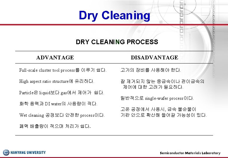
Wet Cleaning WET CLEANING PROCESS Semiconductor Materials Laboratory 23
Dry Cleaning ◆ Dry Wafer Cleaning ⇒ cleaning method carried out in the gas or vapor phase ▶ Requirements of dry wafer cleaning technology 1) Can remove heavy, transition, and alkali metals which are the most difficult to volatilize 2) Not roughen the semiconductor surface nor generate defects in the oxide 3) Not generate solid residues that remain on the cleaned surface 4) Must have high throughput 5) Effective at fairly low temperature 6) Designed to assure compatibility with cluster tool processing and integrated process Semiconductor Materials Laboratory 24
Dry Cleaning ▶ Mechanism of Dry Wafer Cleaning Chemical reaction Momentum transfer Accelerated incident ions Chemically reactive species Volatile compounds Si a) Physical gas-phase cleaning removal of contaminants : by momentum transfer between ions accelerated toward the surface and contaminants species Si b) Chemical dry cleaning better selectivity and reduce a risk of contaminant redeposition reduce the surface damage Semiconductor Materials Laboratory 25
Dry Cleaning ▶ Mechanism of metal contaminants removal Lift- off Si-Cl Evaporation Cl radical M-Cl Reduced pressure Si a) Lift off mechanism - metal chlorides are more volatile than other metal halides Elevated temperature Si b) Evaporation mechanism - due to the random nature of interactions - at the elaborated temperature and reduced pressure Semiconductor Materials Laboratory 26
Dry Cleaning ◆ Dry cleaning 의 연구현황 GROSS 유기물 건식세정방식 FINE 유기물 금속 산화물 물리적방식 LOW ENERGY 스퍼터링 가열방식 HCl H 2 어닐링 HIGH T/UHV MID T/UHV Ge. H 4 : H 2 HCl : HF : H 2 O VAPOR HF : CH 3 OH UV/Cl 2 UV/HF : CH 3 OH UV/NF 3 : H 2 : Ar REMOTE PLASMA HCl REMOTE PLASMA H 2 ECR PLASMA NF 3 or H 2 REMOTE PLASMA NF 3 : H 2 산화 산화 기상방식 UV/오존 플라즈마방식 DIRECT PLASMA O 2 REMOTE PLASMA O 2 UV/오존 UV/O 2 H 2 O VAPOR REMOTE PLASMA O 2 Semiconductor Materials Laboratory 27
Dry Cleaning ◆ Categories of dry wafer cleaning 1) Physical interactions 2) Physically-enhanced chemical reactions 3) Chemical thermal reaction 4) Mechanical technique ▶ Contaminants removal by dry cleaning 1) Organic contaminants : volatilization, UV/O 3 reaction, remote or downstream oxygen plasma treatment 2) Native and chemical oxide, silicate glasses : chemical etching, physical sputter etching, low-energy ECR plasma etching 3) Metal and absorbed ions : remote plasma, photo-induced reaction 4) Particle : vapor etching Semiconductor Materials Laboratory 28
Dry Cleaning ◆ Photochemically-Enhanced Cleaning Low pressure vapor UV lamps as the radiation sources energies required for efficient photolysis Uniform high intensities for wavelengths (150 ~ 600 nm) ▶ UV/O 3 cleaning Oxidize and volatilize organics from surface Pre-oxidation surface treatment Organic removal prior to metallization Surface carbon and hydrocarbon removal Strip photoresist Remove polymer films after RIE process Semiconductor Materials Laboratory 29
Dry Cleaning UV lamp Dry air O 2 O 3 + O H C H oxide Si Si wafer H CO 2 + H 2 O Schematic illustration of the hydrocarbon removal by UV/ozon Organic contaminants + h exited organic contaminants (200~300 nm UV) O 2 + h 2 O (184. 9 nm UV) O + O 2 O 3 + h O + O 2 (253. 7 nm UV) exited organic contaminants + ( O, O 3 ) volatile compounds Semiconductor Materials Laboratory 30
Dry Cleaning UV/O 3 : (a) The result of oxygen removal by B. S. Krusor (USA) (b) The result of carbon removal by H. Jeon (Korea) After UV/O 3 treatment as received a) b) Semiconductor Materials Laboratory 31
Dry Cleaning ▶ UV/Cl 2 Cleaning UV exposure in a Chlorine ambient remove metallic contaminants by volatilization lift metallic contaminants off the surface Not enough to remove alkali metals (Ca, Na…) need additional treatment Not need additional elevated temperature nor reduced pressure Problem : non-uniform, excessive etching of silicon resulting in rough surfaces Semiconductor Materials Laboratory 32
Dry Cleaning ◆ Plasma Enhanced Cleaning Direct plasma cleaning - Ion-induced damage of the substrate Radiation-induced oxide defect - Metallic contaminants and/or alkali ions penetrate the substrate recontaminate the substrate Remote plasma cleaning - By generating an active plasma in a spatial region remote from the substrate - Avoid ion acceleration into the substrate O 2 plasma Remove organic contaminants HCl : Ar plasma Remove metallic contaminants Problem of corrosion NF 3 : H 2 : Ar plasma Etch native/chemical oxide Semiconductor Materials Laboratory 33
Dry Cleaning Remote H 2 plasma : The result of carbon and oxide removal by R. J Markunas (USA) Semiconductor Materials Laboratory 34
Dry Cleaning The effect of metallic contaminants removal by H 2 Plasma cleaning Semiconductor Materials Laboratory 35
Summary and Trend 1970 년대 RCA cleaning 1980 년대 Modified RCA cleaning 농도, 온도, 세정액 Megasonic 채용 1990 년대 Wet cleaning (Ultra clean technology) Ozonized DI water, upw, Surfactant 첨가 Chemical 사용량과 cleaning step을 줄인 새로운 세정방법 Dry cleaning Vapor phase cleaning Plasma cleaning HF-vapor system H-ECR plasma H-remote plasma Cluster Tool 도입 Oxidation과 Cleaning Tool이 연결된 System Semiconductor Materials Laboratory 37
Future Direction ◆ Future direction in Wafer Cleaning 1) Use of super-pure chemicals, gases and DI water 2) Cleaner equipment, and fab facilities Reduce the micro particle 3) Innovative analytical methods : detecting, measuring, and monitoring ultratrace surface contaminants and microparticles 4) Fully-automated system and cluster tool process 5) High product, high reliance, space saving, and low cost process 6) General reduction of liquid chemicals and gases for processing and ecology reasons Semiconductor Materials Laboratory 38