APV 25 wafer testing Outline Wafer test procedure
- Slides: 13

APV 25 wafer testing Outline Wafer test procedure speed improvements feedback from hybrid tests Wafer test results update on results/problems with production lots received so far summary of current position on yield investigations Mark Raymond, Imperial College m. raymond@ic. ac. uk July, 2002 CMS Tracker Electronics 1

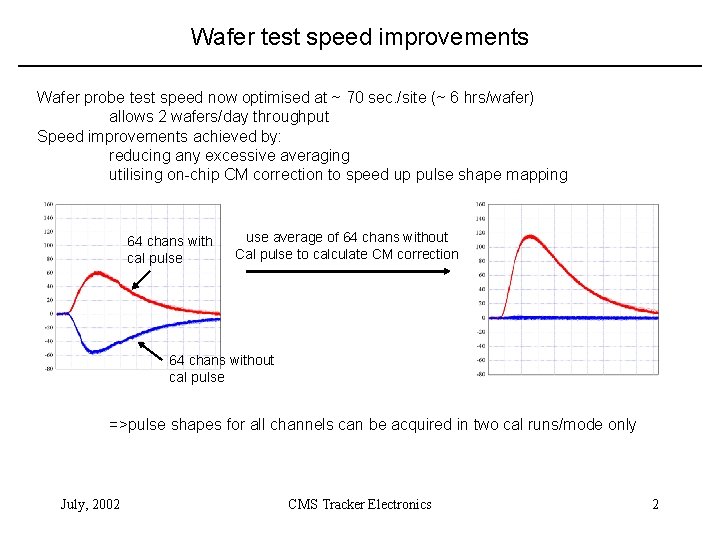
Wafer test speed improvements Wafer probe test speed now optimised at ~ 70 sec. /site (~ 6 hrs/wafer) allows 2 wafers/day throughput Speed improvements achieved by: reducing any excessive averaging utilising on-chip CM correction to speed up pulse shape mapping 64 chans with cal pulse use average of 64 chans without Cal pulse to calculate CM correction 64 chans without cal pulse =>pulse shapes for all channels can be acquired in two cal runs/mode only July, 2002 CMS Tracker Electronics 2

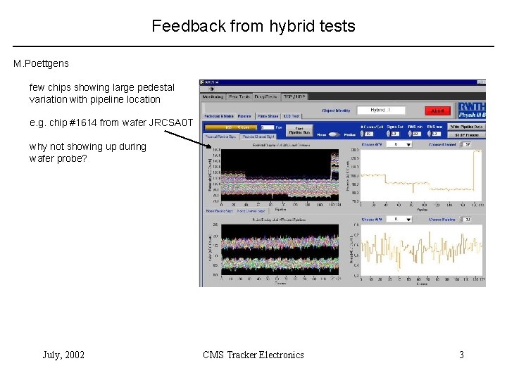
Feedback from hybrid tests M. Poettgens few chips showing large pedestal variation with pipeline location e. g. chip #1614 from wafer JRCSA 0 T why not showing up during wafer probe? July, 2002 CMS Tracker Electronics 3

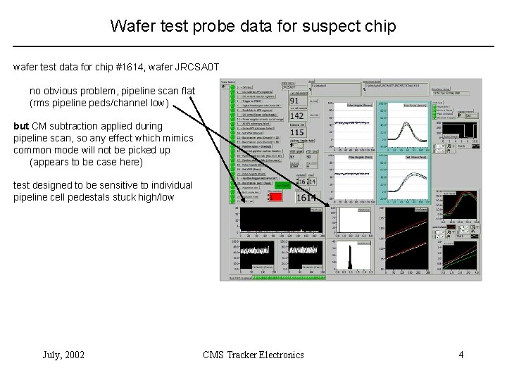
Wafer test probe data for suspect chip wafer test data for chip #1614, wafer JRCSA 0 T no obvious problem, pipeline scan flat (rms pipeline peds/channel low) but CM subtraction applied during pipeline scan, so any effect which mimics common mode will not be picked up (appears to be case here) test designed to be sensitive to individual pipeline cell pedestals stuck high/low July, 2002 CMS Tracker Electronics 4

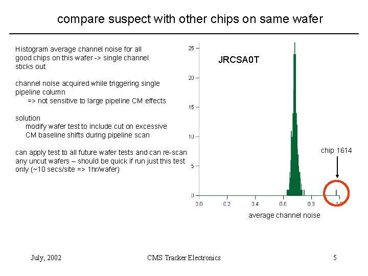
compare suspect with other chips on same wafer Histogram average channel noise for all good chips on this wafer -> single channel sticks out JRCSA 0 T channel noise acquired while triggering single pipeline column => not sensitive to large pipeline CM effects solution modify wafer test to include cut on excessive CM baseline shifts during pipeline scan chip 1614 can apply test to all future wafer tests and can re-scan any uncut wafers – should be quick if run just this test only (~10 secs/site => 1 hr/wafer) average channel noise July, 2002 CMS Tracker Electronics 5

APV 25 wafer testing status Update on previous info presented in May CMS electronics week see http: //www. hep. ph. ic. ac. uk/~dmray/pptfiles/CMS_elec_wk_2002. ppt first 10 engineering wafers (September, 2000) all diced, ~1300 KGD still available at IC 2 production wafer lots delivered January: 48 ordered, 24 + 21 = 45 delivered shortfall of 3 (rejected by manufacturer QA) processing problem – these 2 lots returned to manufacturer 3 rd full lot launched to provide remaining shortfall of 3 (25 wafers/lot) 3 wafers delivered mid Feb. , remaining 22 requested and delivered in March 3 further lots launched to investigate process problems (75 wafers in total) 45 replacement wafers (from 2 lots) now received July, 2002 CMS Tracker Electronics 6

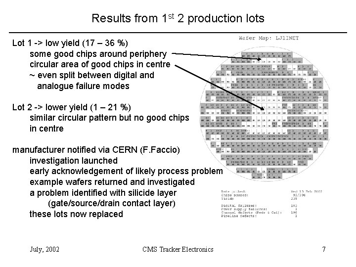
Results from 1 st 2 production lots Lot 1 -> low yield (17 – 36 %) some good chips around periphery circular area of good chips in centre ~ even split between digital and analogue failure modes Lot 2 -> lower yield (1 – 21 %) similar circular pattern but no good chips in centre manufacturer notified via CERN (F. Faccio) investigation launched early acknowledgement of likely process problem example wafers returned and investigated a problem identified with silicide layer (gate/source/drain contact layer) these lots now replaced July, 2002 CMS Tracker Electronics 7

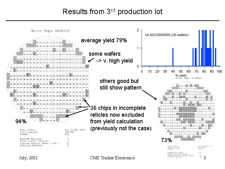
Results from 3 rd production lot average yield 79% some wafers -> v. high yield others good but still show pattern 94% 36 chips in incomplete reticles now excluded from yield calculation (previously not the case) 73% July, 2002 CMS Tracker Electronics 8

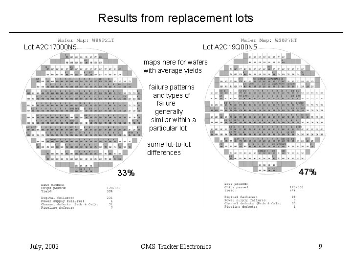
Results from replacement lots Lot A 2 C 17000 N 5 Lot A 2 C 19 Q 00 N 5 maps here for wafers with average yields failure patterns and types of failure generally similar within a particular lot some lot-to-lot differences 47% 33% July, 2002 CMS Tracker Electronics 9

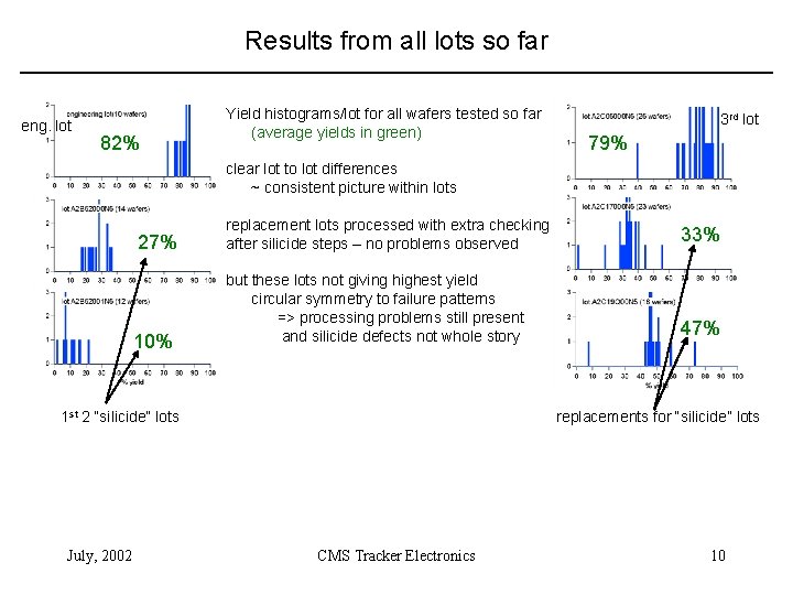
Results from all lots so far eng. lot 82% Yield histograms/lot for all wafers tested so far (average yields in green) 3 rd lot 79% clear lot to lot differences ~ consistent picture within lots 27% 10% replacement lots processed with extra checking after silicide steps – no problems observed 33% but these lots not giving highest yield circular symmetry to failure patterns => processing problems still present and silicide defects not whole story 47% 1 st 2 “silicide” lots July, 2002 replacements for “silicide” lots CMS Tracker Electronics 10

Yield investigations/discussions with manufacturer brief summary of discussion during 0. 25 mm User Group Meeting – June 17 th problem not confined to APV wafers, 3 other HEP designs have also seen similar effects but manufacturer’s volume production not affected any common features in HEP designs? not obvious but long metal lines are possible common feature -> antenna effect (ESD sensitivity) although we are well within design rules v. large”handcrafted” layouts unusual in industry, metal layers auto-filled to higher density our metal layers less densely filled (still within design rules) -> possible under-etching? general conclusion exact cause of problem still unclear work in progress CERN test structure to investigate above theories in preparation examine test results in conjunction with layout looking for evidence to validate theories – inconclusive so far, but still ongoing July, 2002 CMS Tracker Electronics 11

Tested chip availability present chip (KGD) availability + + 1300 3800 remaining chips from engineering run 13 wafers diced from 3 rd lot 5100 in waffle packs now 3300 6300 KGD on remaining uncut 3 rd lot wafers KGD on replacement 45 wafers (assuming we keep) 16800 currently in-hand 3 wafer lots launched to replace 1 st two and investigate problems so more available July, 2002 CMS Tracker Electronics 12

Conclusions Wafer test protocol speed improvements now allow 2 wafers /day feedback from hybrid tests will allow any loopholes to be plugged Wafer probing process problems with first two production lots – attributed to silicide problem wafers returned and replaced communication channel (via CERN) to manufacturer effective manufacturer’s response very constructive and helpful throughout 3 rd lot yield back at expected high level (average 79%) replacement lots not maintaining high yield (33% and 47%) and not silicide reasons for low yield not fully understood – more work in progress July, 2002 CMS Tracker Electronics 13