APV 25 Production Testing Quality Assurance APV 25
- Slides: 27

APV 25 Production Testing & Quality Assurance APV 25 – 0. 25 mm CMOS readout chip for CMS Si Tracker Production wafer probe testing (Imperial College) results from wafers tested so far Production quality assurance (IC and Padova) QA plan and results for chips sampled from production wafers M. Raymond, R. Bainbridge, G. Hall, E. Noah, J. Leaver, Imperial College London, UK. M. French, Rutherford Appleton Laboratory, UK. A. Candelori, A. Kaminsky, Universita di Padova, Italy. 8 th Workshop on Electronics for LHC Experiments, Colmar, France, September, 2002 LHC Electronics Workshop, Colmar 1

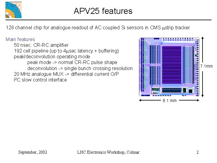
APV 25 features 128 channel chip for analogue readout of AC coupled Si sensors in CMS mstrip tracker Main features 50 nsec. CR-RC amplifier 192 cell pipeline (up to 4 msec latency + buffering) peak/deconvolution operating mode peak mode -> normal CR-RC pulse shape deconvolution -> single bunch crossing resolution 20 MHz analogue MUX -> differential current O/P I 2 C slow control interface 7. 1 mm 8. 1 mm September, 2002 LHC Electronics Workshop, Colmar 2

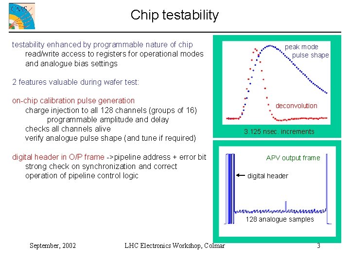
Chip testability enhanced by programmable nature of chip read/write access to registers for operational modes and analogue bias settings peak mode pulse shape 2 features valuable during wafer test: on-chip calibration pulse generation charge injection to all 128 channels (groups of 16) programmable amplitude and delay checks all channels alive verify analogue pulse shape (and tune if required) digital header in O/P frame ->pipeline address + error bit strong check on synchronization and correct operation of pipeline control logic deconvolution 3. 125 nsec. increments APV output frame digital header 128 analogue samples September, 2002 LHC Electronics Workshop, Colmar 3

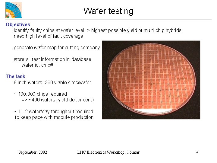
Wafer testing Objectives identify faulty chips at wafer level -> highest possible yield of multi-chip hybrids need high level of fault coverage generate wafer map for cutting company store all test information in database wafer id, chip# The task 8 inch wafers, 360 viable sites/wafer ~ 100, 000 chips required => ~400 wafers (yield dependent) ~ 1 - 2 wafer/day throughput required to keep pace with module production September, 2002 LHC Electronics Workshop, Colmar 4

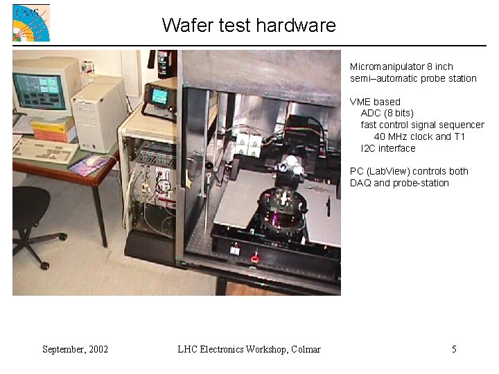
Wafer test hardware Micromanipulator 8 inch semi–automatic probe station VME based ADC (8 bits) fast control signal sequencer 40 MHz clock and T 1 I 2 C interface PC (Lab. View) controls both DAQ and probe-station September, 2002 LHC Electronics Workshop, Colmar 5

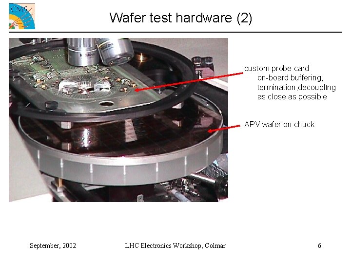
Wafer test hardware (2) custom probe card on-board buffering, termination, decoupling as close as possible APV wafer on chuck September, 2002 LHC Electronics Workshop, Colmar 6

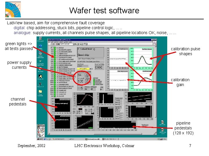
Wafer test software Lab. View based, aim for comprehensive fault coverage digital: chip addressing, stuck bits, pipeline control logic, …. . analogue: supply currents, all channels pulse shapes, all pipeline locations OK, noise, …… green lights => all tests passed calibration pulse shapes power supply currents calibration gain channel pedestals pipeline pedestals (128 x 192) September, 2002 LHC Electronics Workshop, Colmar 7

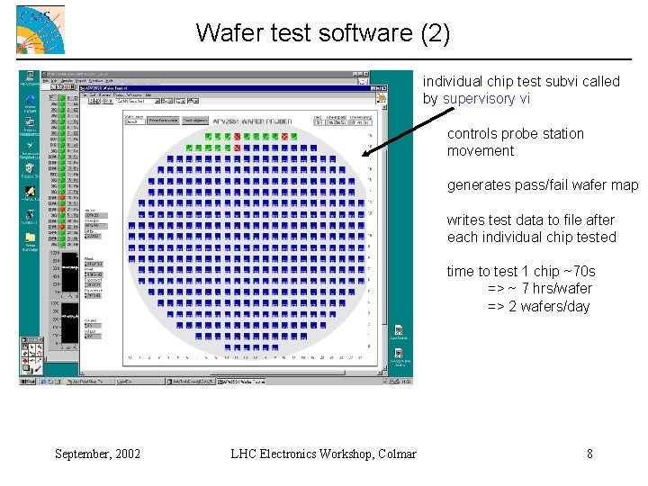
Wafer test software (2) individual chip test subvi called by supervisory vi controls probe station movement generates pass/fail wafer map writes test data to file after each individual chip tested time to test 1 chip ~70 s => ~ 7 hrs/wafer => 2 wafers/day September, 2002 LHC Electronics Workshop, Colmar 8

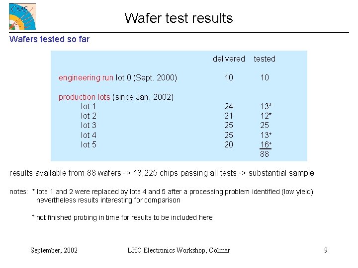
Wafer test results Wafers tested so far delivered tested engineering run lot 0 (Sept. 2000) 10 10 production lots (since Jan. 2002) lot 1 lot 2 lot 3 lot 4 lot 5 24 21 25 25 20 13* 12* 25 13+ 16+ 88 results available from 88 wafers -> 13, 225 chips passing all tests -> substantial sample notes: * lots 1 and 2 were replaced by lots 4 and 5 after a processing problem identified (low yield) nevertheless results interesting for comparison + not finished probing in time for results to be included here September, 2002 LHC Electronics Workshop, Colmar 9

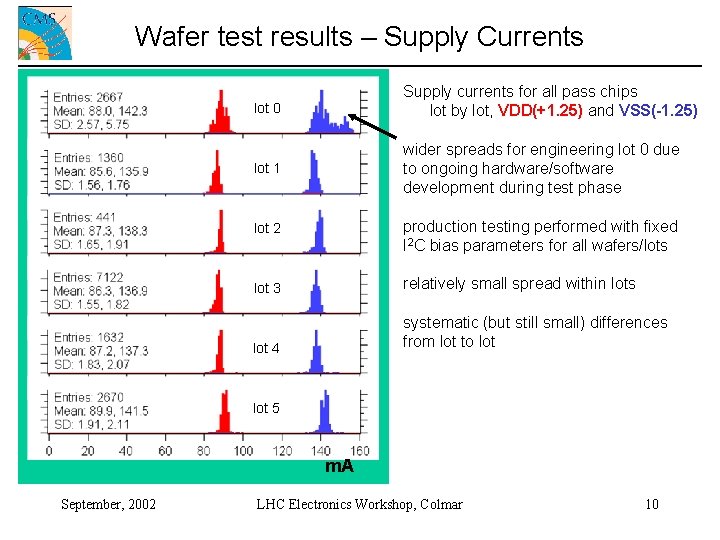
Wafer test results – Supply Currents Supply currents for all pass chips lot by lot, VDD(+1. 25) and VSS(-1. 25) lot 0 wider spreads for engineering lot 0 due to ongoing hardware/software development during test phase lot 1 lot 2 production testing performed with fixed I 2 C bias parameters for all wafers/lots lot 3 relatively small spread within lots lot 4 systematic (but still small) differences from lot to lot 5 m. A September, 2002 LHC Electronics Workshop, Colmar 10

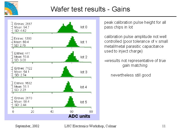
Wafer test results - Gains lot 0 lot 1 lot 2 lot 3 peak calibration pulse height for all pass chips in lot calibration pulse amplitude not well controlled (poor tolerance of v. small metal/metal parasitic capacitance used to inject charge) Þresults not representative of true gain matching nevertheless still good lot 4 lot 5 ADC units September, 2002 LHC Electronics Workshop, Colmar 11

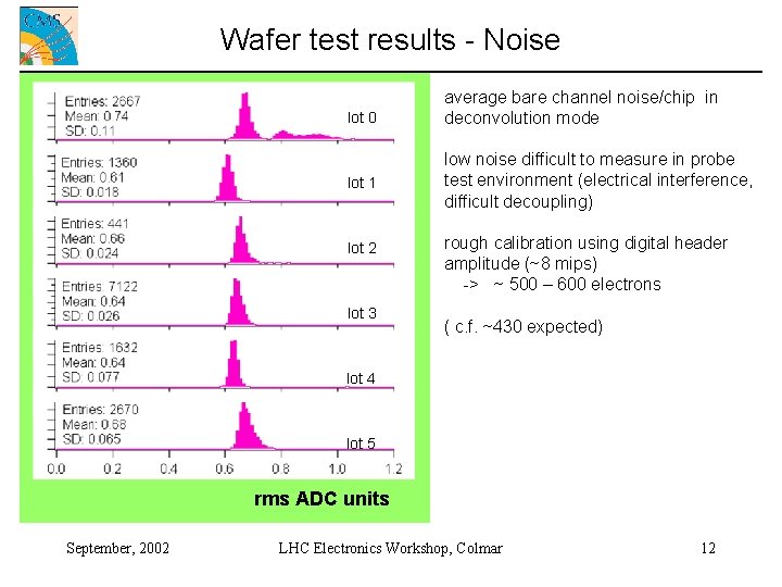
Wafer test results - Noise lot 0 lot 1 lot 2 lot 3 average bare channel noise/chip in deconvolution mode low noise difficult to measure in probe test environment (electrical interference, difficult decoupling) rough calibration using digital header amplitude (~8 mips) -> ~ 500 – 600 electrons ( c. f. ~430 expected) lot 4 lot 5 rms ADC units September, 2002 LHC Electronics Workshop, Colmar 12

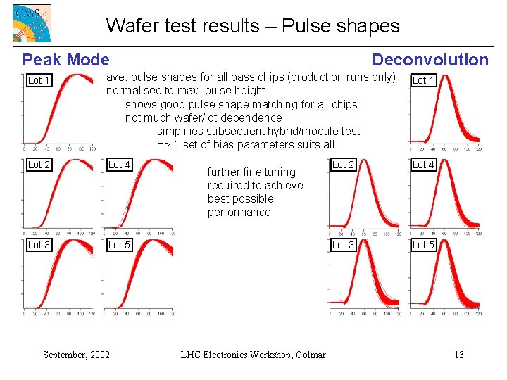
Wafer test results – Pulse shapes Peak Mode Deconvolution Lot 1 ave. pulse shapes for all pass chips (production runs only) normalised to max. pulse height shows good pulse shape matching for all chips not much wafer/lot dependence simplifies subsequent hybrid/module test => 1 set of bias parameters suits all Lot 1 Lot 2 Lot 4 Lot 3 Lot 5 September, 2002 further fine tuning required to achieve best possible performance LHC Electronics Workshop, Colmar 13

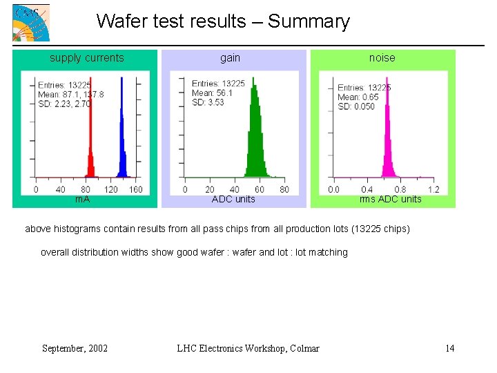
Wafer test results – Summary supply currents m. A gain ADC units noise rms ADC units above histograms contain results from all pass chips from all production lots (13225 chips) overall distribution widths show good wafer : wafer and lot : lot matching September, 2002 LHC Electronics Workshop, Colmar 14

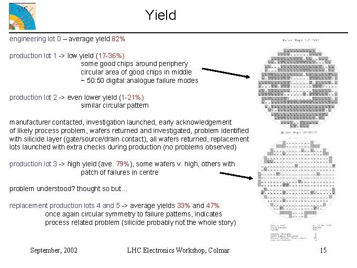
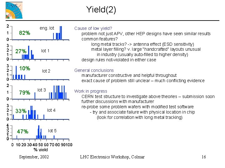
Yield engineering lot 0 – average yield 82% production lot 1 -> low yield (17 -36%) some good chips around periphery circular area of good chips in middle ~ 50: 50 digital: analogue failure modes production lot 2 -> even lower yield (1 -21%) similar circular pattern manufacturer contacted, investigation launched, early acknowledgement of likely process problem, wafers returned and investigated, problem identified with silicide layer (gate/source/drain contact), all wafers returned, replacement lots launched with extra checks during production (no problems observed) production lot 3 -> high yield (ave. 79%), some wafers v. high, others with patch of failures in centre problem understood? thought so but… replacement production lots 4 and 5 -> average yields 33% and 47% once again circular symmetry to failure patterns, indicates process related problem (silicide probably not the whole story) September, 2002 LHC Electronics Workshop, Colmar 15

Yield(2) 82% 27% 10% 79% 33% 47% eng. lot 1 lot 2 lot 3 lot 4 Cause of low yield? problem not just APV, other HEP designs have seen similar results common features? long metal tracks? -> antenna effect (ESD sensitivity) metal layer filling? v. large “handcrafted” layouts unusual in industry (usually auto-filled to higher density) design rules not-violated in either case General conclusions manufacturer constructive and helpful throughout exact cause of problem still unclear – much conflicting evidence Work in progress CERN test structure to investigate above theories – submission soon further discussions with manufacturer re-probe some problem wafers with modified test software - try and associate failure with physical location in chip (look for correlation with long metal tracking) lot 5 September, 2002 LHC Electronics Workshop, Colmar 16

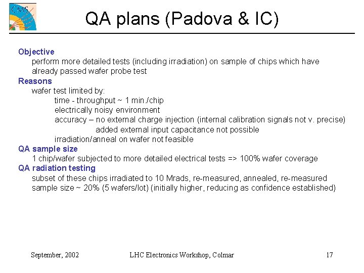
QA plans (Padova & IC) Objective perform more detailed tests (including irradiation) on sample of chips which have already passed wafer probe test Reasons wafer test limited by: time - throughput ~ 1 min. /chip electrically noisy environment accuracy – no external charge injection (internal calibration signals not v. precise) added external input capacitance not possible irradiation/anneal on wafer not feasible QA sample size 1 chip/wafer subjected to more detailed electrical tests => 100% wafer coverage QA radiation testing subset of these chips irradiated to 10 Mrads, re-measured, annealed, re-measured sample size ~ 20% (5 wafers/lot) (initially higher, reducing as confidence established) September, 2002 LHC Electronics Workshop, Colmar 17

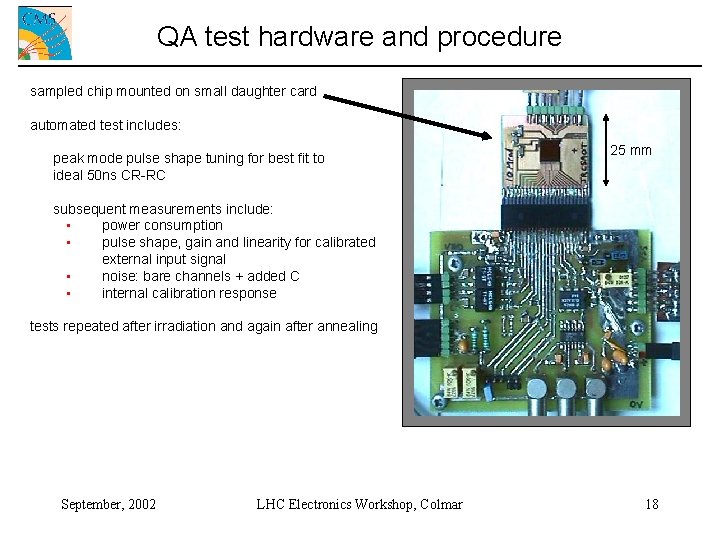
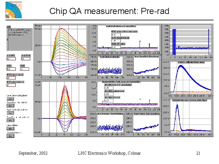
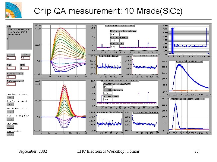
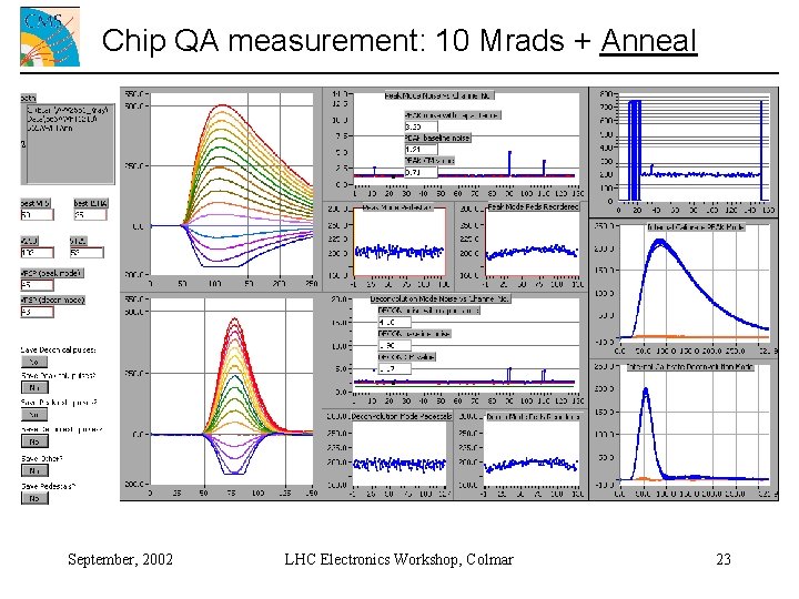
QA test hardware and procedure sampled chip mounted on small daughter card automated test includes: peak mode pulse shape tuning for best fit to ideal 50 ns CR-RC 25 mm subsequent measurements include: • power consumption • pulse shape, gain and linearity for calibrated external input signal • noise: bare channels + added C • internal calibration response tests repeated after irradiation and again after annealing September, 2002 LHC Electronics Workshop, Colmar 18

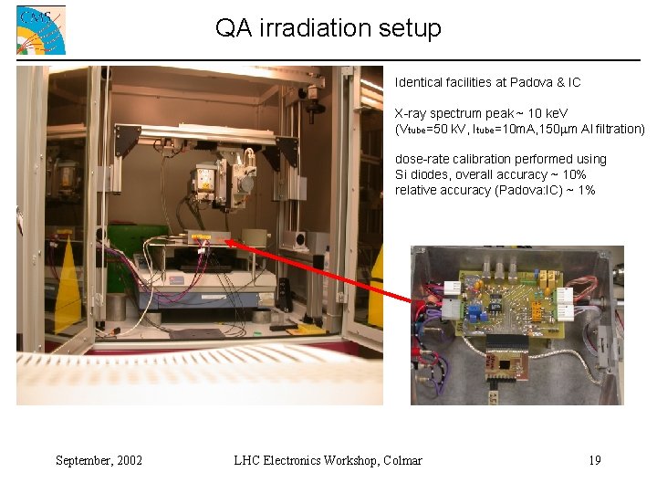
QA irradiation setup Identical facilities at Padova & IC X-ray spectrum peak ~ 10 ke. V (Vtube=50 k. V, Itube=10 m. A, 150 mm Al filtration) dose-rate calibration performed using Si diodes, overall accuracy ~ 10% relative accuracy (Padova: IC) ~ 1% September, 2002 LHC Electronics Workshop, Colmar 19

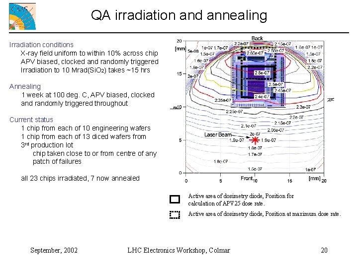
QA irradiation and annealing Irradiation conditions X-ray field uniform to within 10% across chip APV biased, clocked and randomly triggered Irradiation to 10 Mrad(Si. O 2) takes ~15 hrs Annealing 1 week at 100 deg. C, APV biased, clocked and randomly triggered throughout Current status 1 chip from each of 10 engineering wafers 1 chip from each of 13 diced wafers from 3 rd production lot chip taken close to or from centre of any patch of failures all 23 chips irradiated, 7 now annealed Active area of dosimetry diode, Position for calculation of APV 25 dose rate. Active area of dosimetry diode, Position at maximum dose rate. September, 2002 LHC Electronics Workshop, Colmar 20

Chip QA measurement: Pre-rad September, 2002 LHC Electronics Workshop, Colmar 21

Chip QA measurement: 10 Mrads(Si. O 2) September, 2002 LHC Electronics Workshop, Colmar 22

Chip QA measurement: 10 Mrads + Anneal September, 2002 LHC Electronics Workshop, Colmar 23

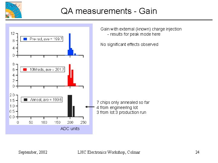
QA measurements - Gain with external (known) charge injection - results for peak mode here No significant effects observed 7 chips only annealed so far 4 from engineering lot 3 from lot 3 production run ADC units September, 2002 LHC Electronics Workshop, Colmar 24

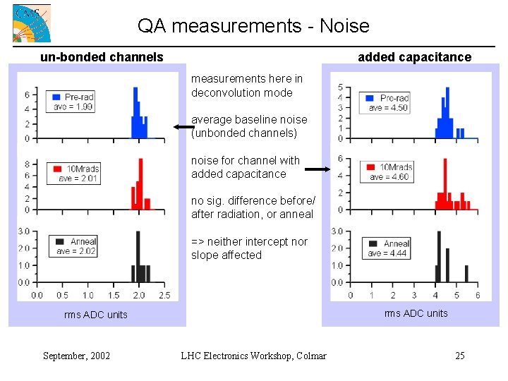
QA measurements - Noise un-bonded channels added capacitance measurements here in deconvolution mode average baseline noise (unbonded channels) noise for channel with added capacitance no sig. difference before/ after radiation, or anneal => neither intercept nor slope affected rms ADC units September, 2002 LHC Electronics Workshop, Colmar 25

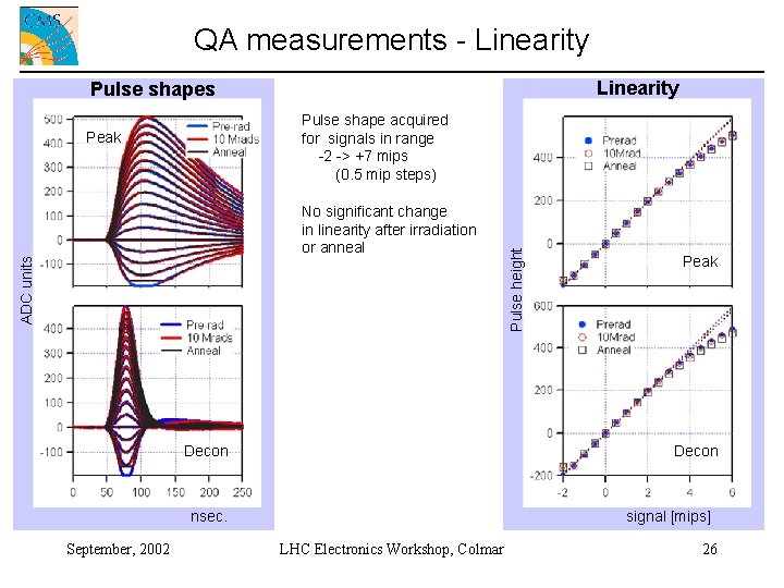
QA measurements - Linearity Pulse shapes Peak ADC units No significant change in linearity after irradiation or anneal Decon Peak Decon nsec. September, 2002 Pulse height Pulse shape acquired for signals in range -2 -> +7 mips (0. 5 mip steps) signal [mips] LHC Electronics Workshop, Colmar 26

Conclusions Wafer probing production wafer probe test setup working well throughput 2 wafers/day ~ 100 wafers tested so far (data from analysis of 13, 000 chips presented here) analysis of test data shows good matching between chips, wafers and lots yield problems observed on some lots cause still unclear (some theories) work in progress QA measurements automated measurement setup and protocol developed measurements pre-rad, after 10 Mrads, after anneal results from chips from all 10 engineering run wafers, and 13 of 25 production lot 3 wafers no significant effects observed September, 2002 LHC Electronics Workshop, Colmar 27