Gordon Moores Law 11 Zero Layer IC START


,縮寫為MOSFET 。 19")


 Ω) Resistance ( 250 200 Crack IMC 15 0 100 dominant 50 0")


 O V max Surface Charges (a) Voltage")
 40")
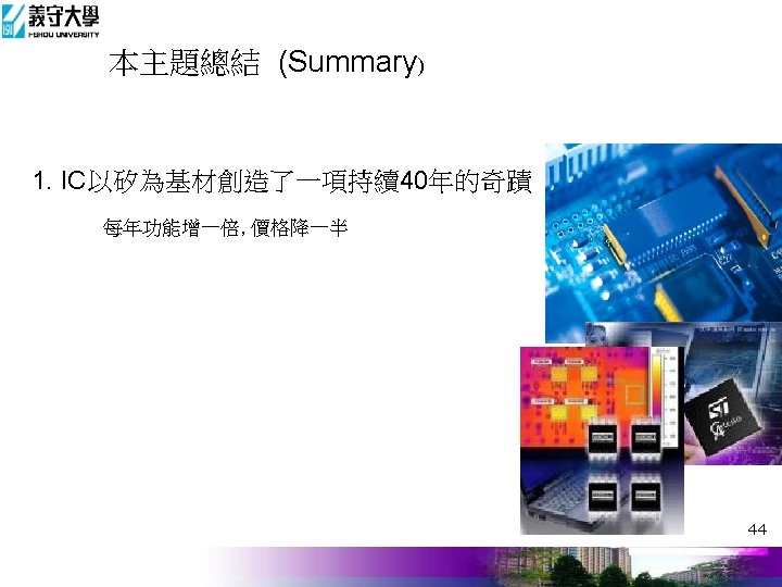

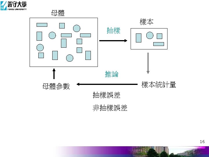
- Slides: 45
Gordon Moore’s Law 11
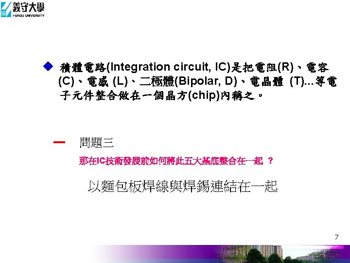
Zero Layer IC電子結構是一層一層加 對準堆疊完成 START OX Zero Layer ETCH Zero Layer PHOTO PR Remove 14
2. Po-Ying Chen*, “Degradation of Gate Oxide Integrity by Formation of Tiny Holes by Metal Contamination during Wafering Process”, Jpn. Journal of Applied Physics, p. 8685 -8690, SCI, N/M=50/94, IF: 2. 85. , IF: 2. 47, (2008) citation: 3 18
6. 材料厚度與均勻度 金氧半場效電晶體 (Metal-Oxide-Semiconductor Field-Effect Transistor),縮寫為MOSFET 。 19
6. 材料厚度與均勻度 -- The gate dielectric layer roughness will reduce the electronic mobility. 2. 5 V for 0. 25 um DR 1. 0 V for 0. 09 um DR e e Rough Si substrate 20
-- The flatness will result-in the patterning lose problem. 7. 晶片平坦度 21
7. 晶片平坦度 -- CMP process will induce nano-topography issue, and this problem will affect the device performance. Oxide Silicon Nanotopography Length 5 mm for example "Stiff" ("Hard") Pad CMP Process Planarization Length ~ 7 - 10 mm CMP • Preferentially thins surface films in raised nanotopography areas. 22
7. 晶片平坦度 Impact on Nano-topography Improved Polishing pad optimized THA 2: 2 x 2 mm 17. 7 nm 9. 3 nm THA 4: 10 x 10 mm 32. 7 nm 21. 9 nm 23
(a) Ω) Resistance ( 250 200 Crack IMC 15 0 100 dominant 50 0 0 5000 10000 15000 Current density J (m. A/cm 2) Ω) Resistance ( (b) 3 2. 5 2 1. 5 1 0 2000 4000 6000 Current density J (m. A/cm 2) 24
Drop tool Si wafer Wafer guide 25
26
27
28
9. 原物料 10. Raw Wafer 11. COP大小分佈圖 29
9. 原物料Raw Wafer BMD Bulk Micron Defect = Voids + O 2 30
9. 原物料Raw Wafer BMD 31
9. 原物料Raw Wafer BMD分佈 32
9. 原物料Raw Wafer BMD 33
9. 原物料Raw Wafer BMD 34
9. 原物料Raw Wafer BMD 35
36
11. 靜電頓對IC製程的影響 X 10 r Accumulation (V) O V max Surface Charges (a) Voltage (b) 12 10 8 6 4 2 0 0 2 4 6 8 10 12 R Distance (inch) 37
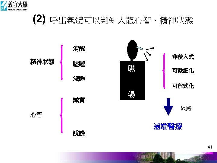
(1) 40
Thanks! 45