Shri Sant Gajanan Maharaj College of Engineering Department
- Slides: 57

Shri Sant Gajanan Maharaj College of Engineering Department of Electronics & Telecommunications Engineering Electronic Devices & Components Unit – V Special Purpose Diodes Tunnel Diode and Photodiode

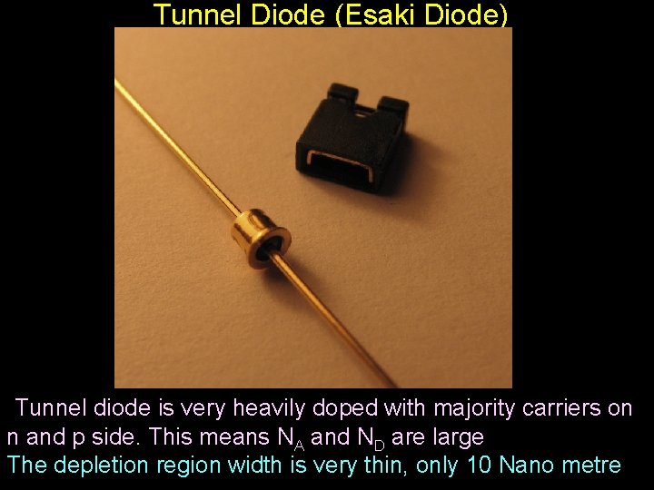
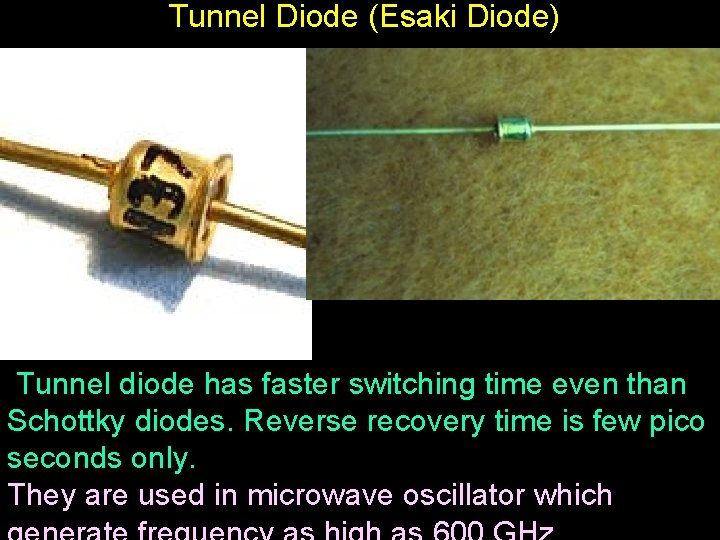
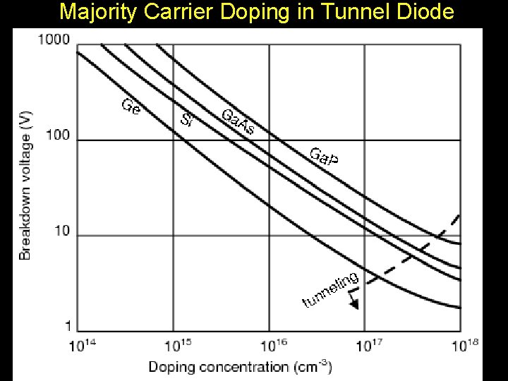
Tunnel Diode (Esaki Diode) Tunnel diode is very heavily doped with majority carriers on n and p side. This means NA and ND are large The depletion region width is very thin, only 10 Nano metre

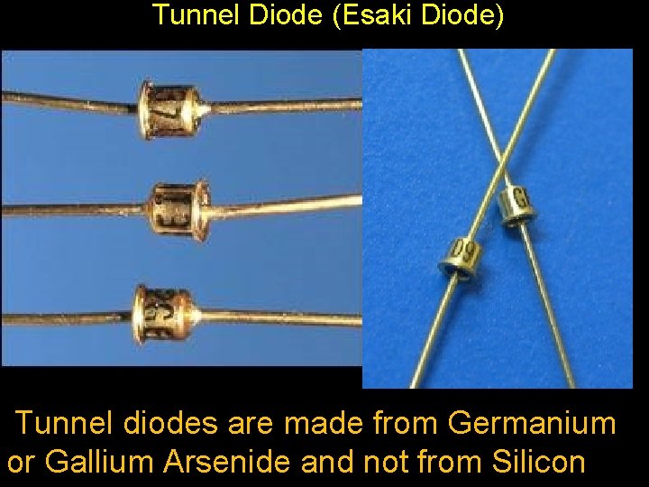
Tunnel Diode (Esaki Diode) Tunnel diodes are made from Germanium or Gallium Arsenide and not from Silicon

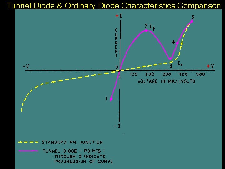
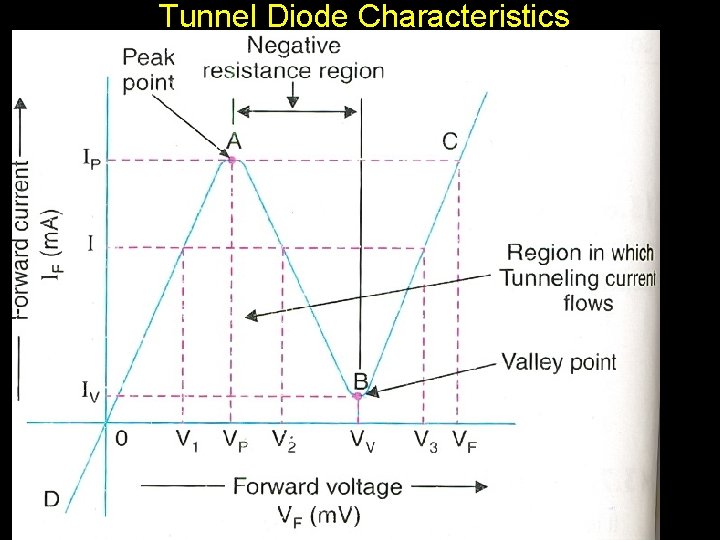
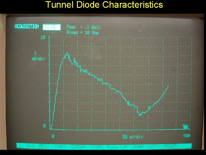
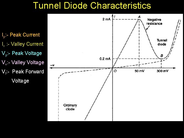
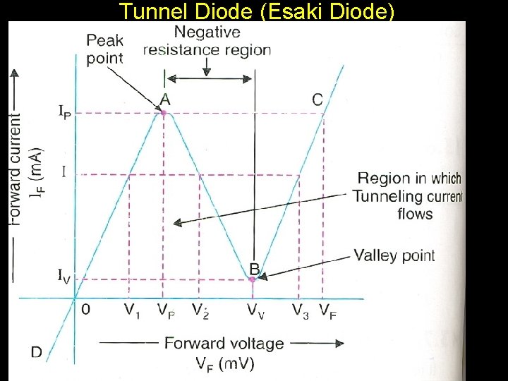
Tunnel Diode (Esaki Diode) The V-I characteristics of Tunnel diode is very different compared to ordinary diode. Tunnel diode characteristics has ‘Negative Resistance Region’

Tunnel Diode (Esaki Diode) Tunnel diode has faster switching time even than Schottky diodes. Reverse recovery time is few pico seconds only. They are used in microwave oscillator which

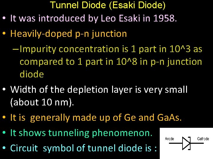
Tunnel Diode (Esaki Diode) • It was introduced by Leo Esaki in 1958. • Heavily-doped p-n junction – Impurity concentration is 1 part in 10^3 as compared to 1 part in 10^8 in p-n junction diode • Width of the depletion layer is very small (about 10 nm). • It is generally made up of Ge and Ga. As. • It shows tunneling phenomenon. • Circuit symbol of tunnel diode is :

Tunnel Diode & Ordinary Diode Characteristics Comparison

Tunnel Diode Characteristics

Tunnel Diode Characteristics

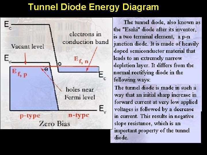
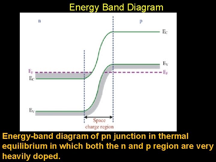
Tunnel Diode Energy Diagram

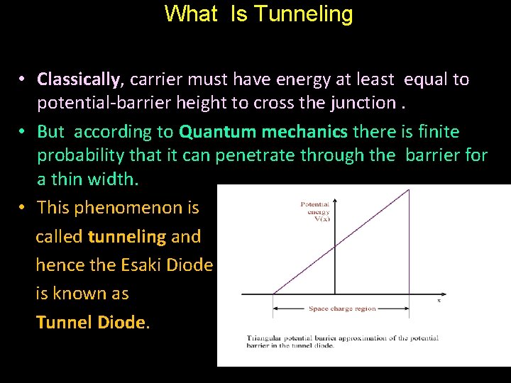
What Is Tunneling • Classically, carrier must have energy at least equal to potential-barrier height to cross the junction. • But according to Quantum mechanics there is finite probability that it can penetrate through the barrier for a thin width. • This phenomenon is called tunneling and hence the Esaki Diode is known as Tunnel Diode.

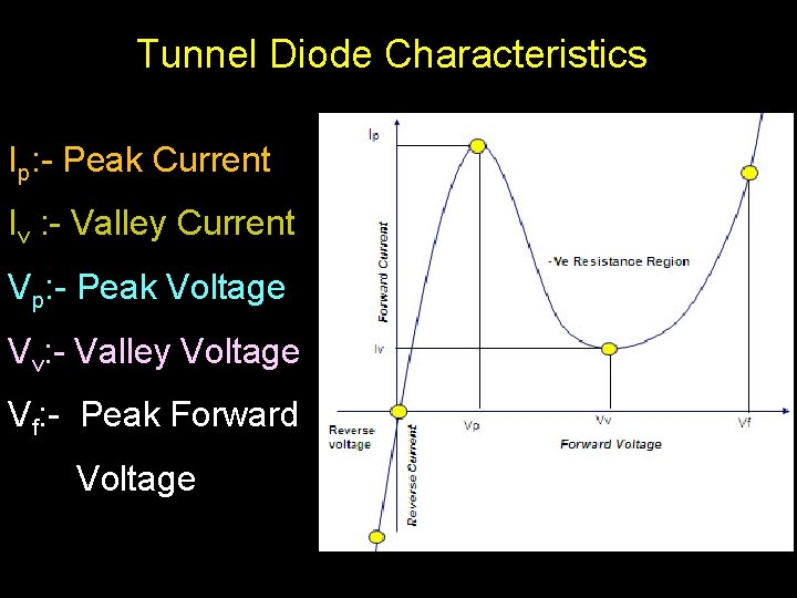
Tunnel Diode Characteristics Ip: - Peak Current Iv : - Valley Current Vp: - Peak Voltage Vv: - Valley Voltage Vf: - Peak Forward Voltage

Tunnel Diode Characteristics Ip: - Peak Current Iv : - Valley Current Vp: - Peak Voltage Vv: - Valley Voltage Vf: - Peak Forward Voltage

Tunnel Diode (Esaki Diode)

Majority Carrier Doping in Tunnel Diode

Energy Band Diagram Energy-band diagram of pn junction in thermal equilibrium in which both the n and p region are very heavily doped.

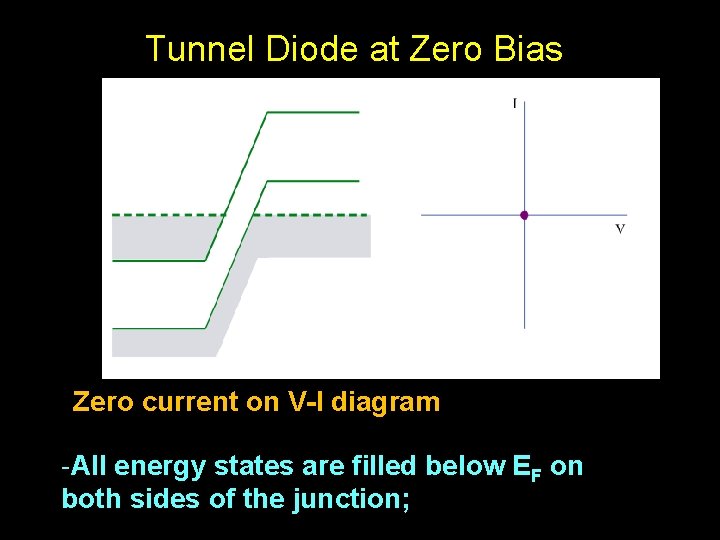
Tunnel Diode at Zero Bias Zero current on V-I diagram -All energy states are filled below EF on both sides of the junction;

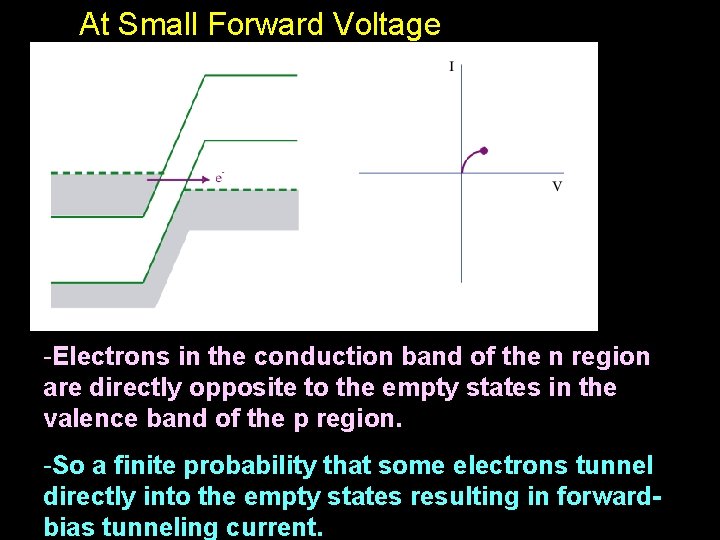
At Small Forward Voltage -Electrons in the conduction band of the n region are directly opposite to the empty states in the valence band of the p region. -So a finite probability that some electrons tunnel directly into the empty states resulting in forwardbias tunneling current.

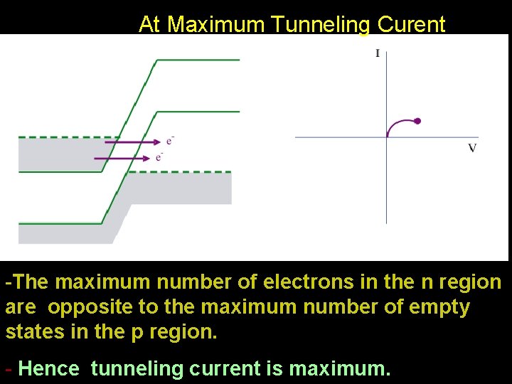
At Maximum Tunneling Curent -The maximum number of electrons in the n region are opposite to the maximum number of empty states in the p region. - Hence tunneling current is maximum.

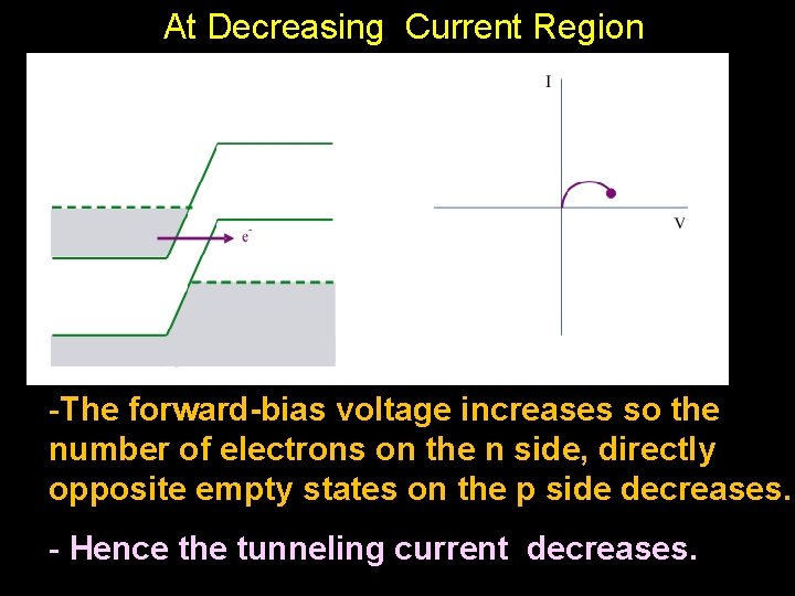
At Decreasing Current Region -The forward-bias voltage increases so the number of electrons on the n side, directly opposite empty states on the p side decreases. - Hence the tunneling current decreases.

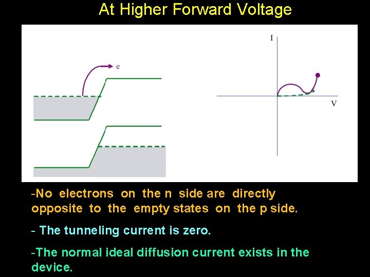
At Higher Forward Voltage -No electrons on the n side are directly opposite to the empty states on the p side. - The tunneling current is zero. -The normal ideal diffusion current exists in the device.

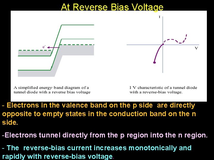
At Reverse Bias Voltage - Electrons in the valence band on the p side are directly opposite to empty states in the conduction band on the n side. -Electrons tunnel directly from the p region into the n region. - The reverse-bias current increases monotonically and rapidly with reverse-bias voltage.

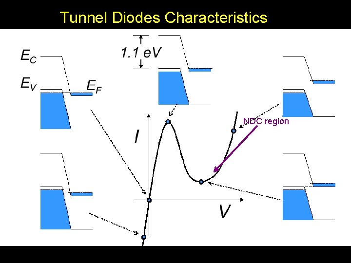
Tunnel Diodes Characteristics NDC region

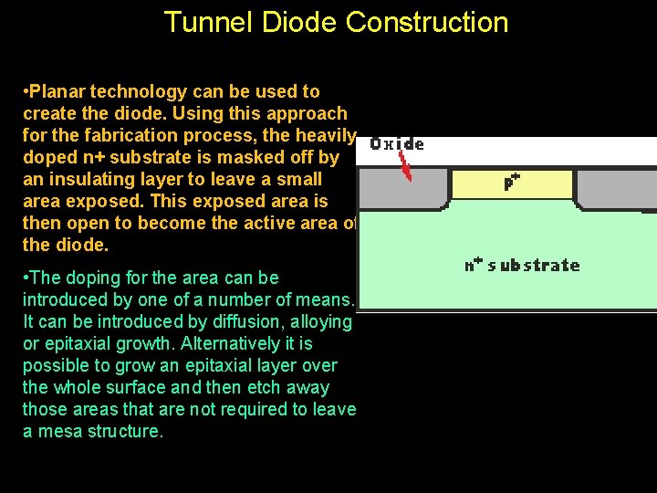
Tunnel Diode Construction • Planar technology can be used to create the diode. Using this approach for the fabrication process, the heavily doped n+ substrate is masked off by an insulating layer to leave a small area exposed. This exposed area is then open to become the active area of the diode. • The doping for the area can be introduced by one of a number of means. It can be introduced by diffusion, alloying or epitaxial growth. Alternatively it is possible to grow an epitaxial layer over the whole surface and then etch away those areas that are not required to leave a mesa structure.

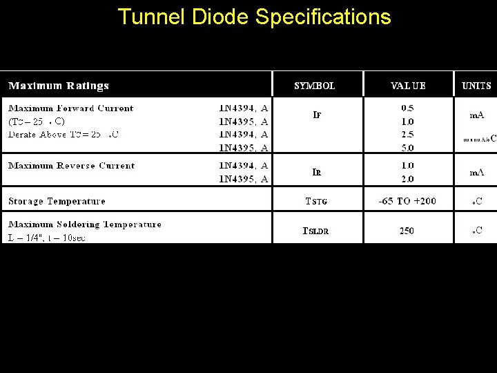
Tunnel Diode Specifications

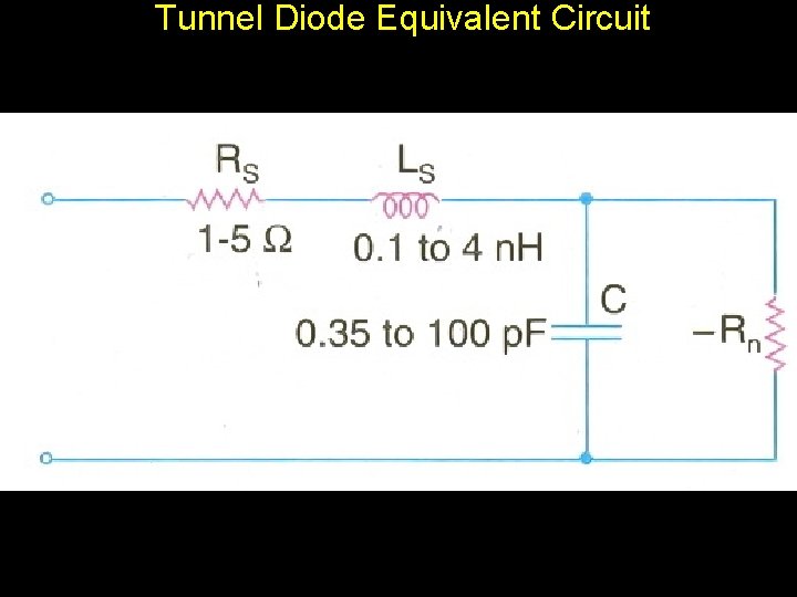
Tunnel Diode Equivalent Circuit

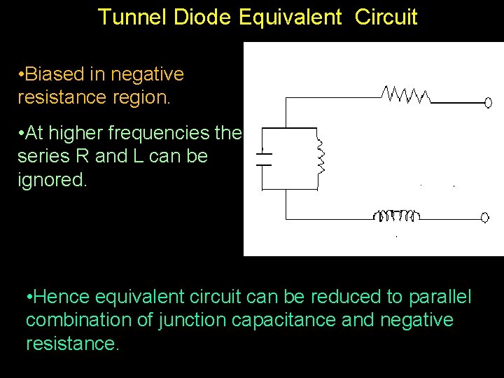
Tunnel Diode Equivalent Circuit • Biased in negative resistance region. • At higher frequencies the series R and L can be ignored. rs Cj -R Ls • Hence equivalent circuit can be reduced to parallel combination of junction capacitance and negative resistance.

Tunnel Diodes Advantages • Very high speed: The high speed of operation means that the tunnel diode can be used for microwave RF applications. • Longevity: Studies have been undertaken of the tunnel diode and its performance has been shown to remain stable over long periods of time, where other semiconductor devices may have degraded.

Tunnel Diode Applications • Microwave frequency range oscillators • Amplifiers • Switch • Logic Gates

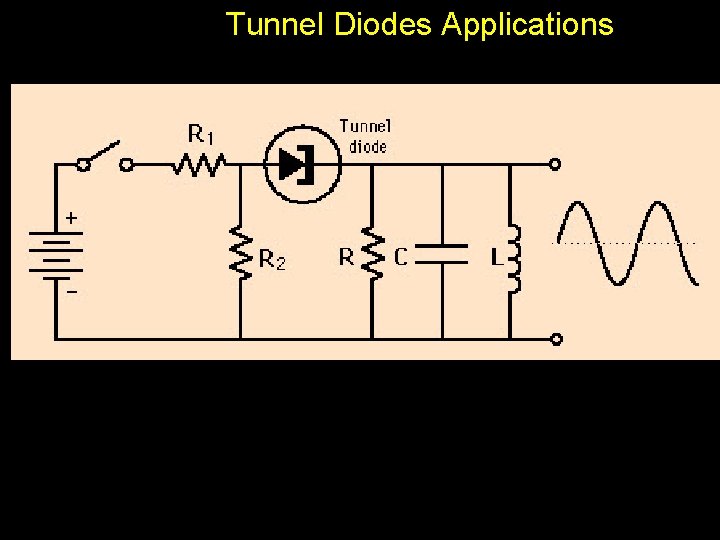
Tunnel Diodes Applications

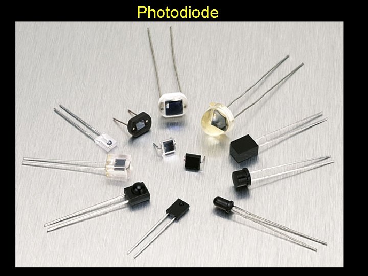
Photodiode

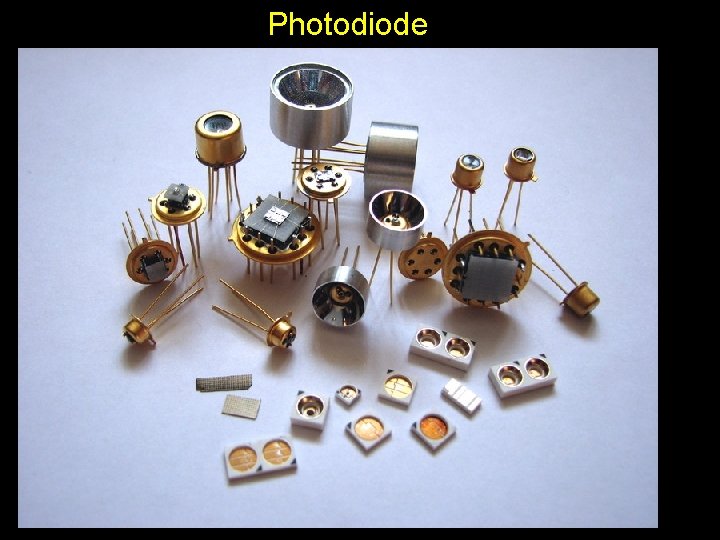
Photodiode

Photodiode

Photodiode

Photodiode

Photodiode

Photodiode

Photodiode

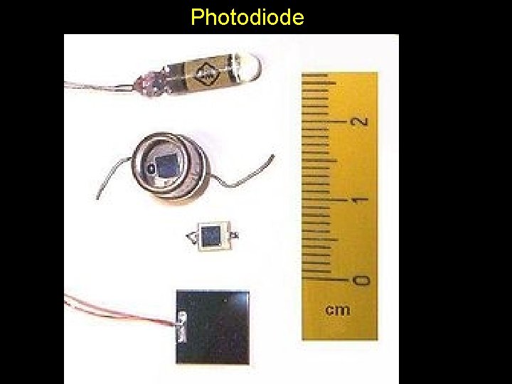
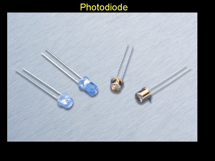
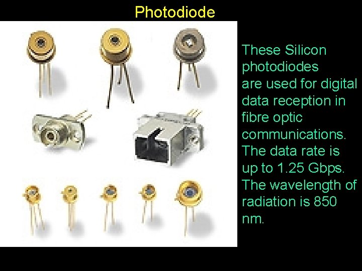
Photodiode These Silicon photodiodes are used for digital data reception in fibre optic communications. The data rate is up to 1. 25 Gbps. The wavelength of radiation is 850 nm.

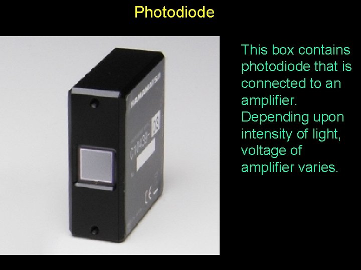
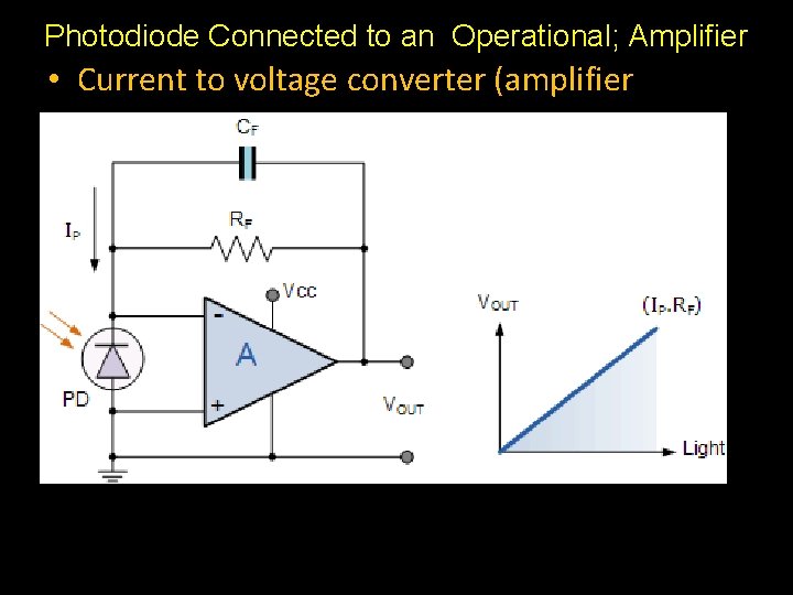
Photodiode This box contains photodiode that is connected to an amplifier. Depending upon intensity of light, voltage of amplifier varies.

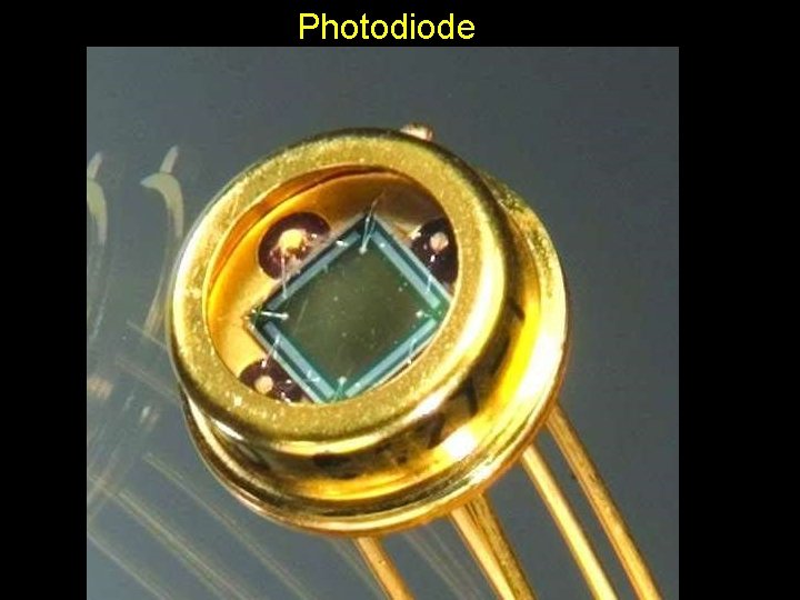
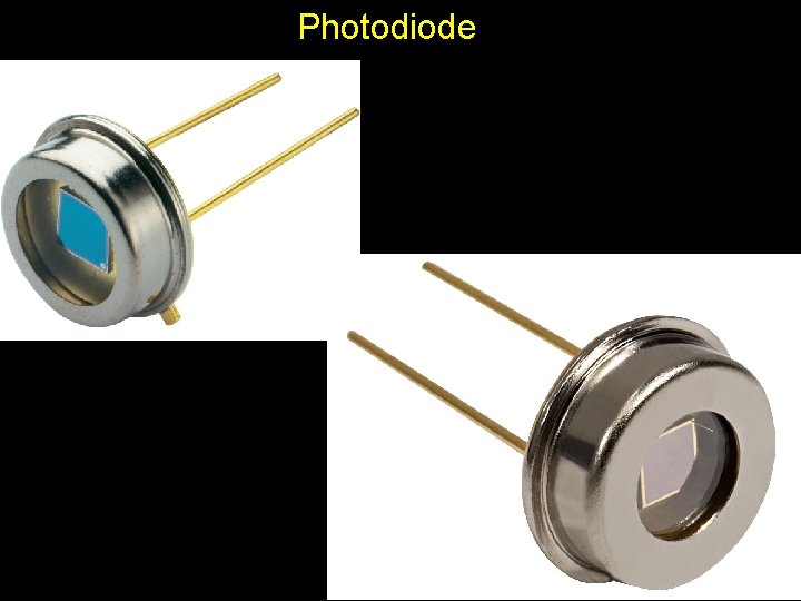
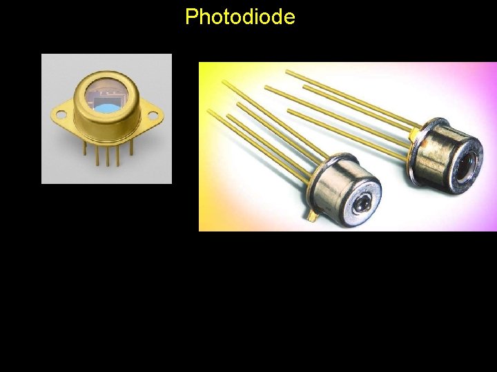
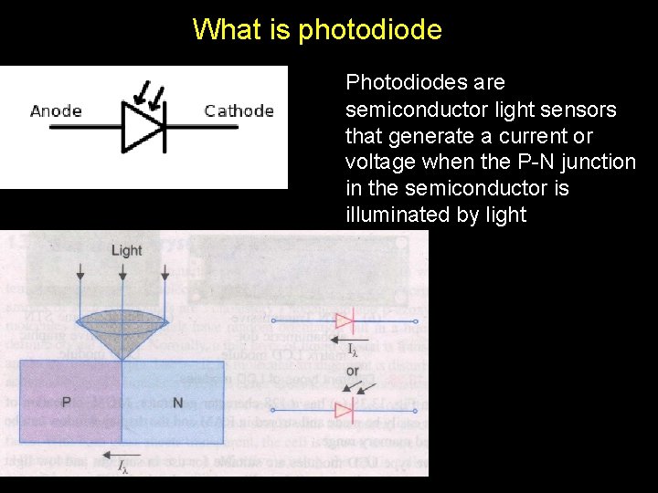
What is photodiode Photodiodes are semiconductor light sensors that generate a current or voltage when the P-N junction in the semiconductor is illuminated by light

Principle of Photodiode Operation A photodiode is a p-n junction or PIN structure. When a photon of sufficient energy strikes the diode, it excites an electron, thereby creating a free electron (and a positively charged electron hole). This mechanism is also known as the inner photoelectric effect. If the absorption occurs in the junction's depletion region, or one diffusion length away from it, these carriers are swept from the junction by the built-in field of the depletion region. Thus holes move toward the anode, and electrons toward the cathode, and a photocurrent is produced. This photocurrent is the sum of both the dark current (without light) and the light current, so the dark current must be minimized to enhance the sensitivity of the device.

Applications of Photodiode They may be used to generate an output which is dependent upon the illumination (analog; for measurement and the like), or to change the state of circuitry Photodiodes are used in consumer electronics devices such as compact disc players, smoke detectors, and the receivers for infrared remote control devices used to control equipment from televisions to air conditioners. Used in camera light meters, or to respond to light levels, as in switching on street lighting after dark. Photodiodes are often used for accurate measurement of light intensity in science and industry. They are also widely used in various medical applications, such as detectors for computed tomography. 43

Features of photodiode • Excellent linearity with respect to incident light • Low noise • Wide spectral response • Mechanically rugged • Compact and lightweight Long life

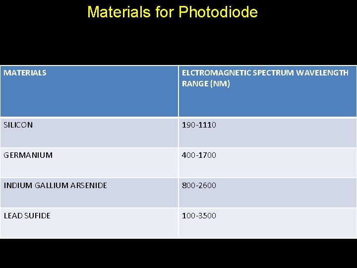
Materials for Photodiode MATERIALS ELCTROMAGNETIC SPECTRUM WAVELENGTH RANGE (NM) SILICON 190 -1110 GERMANIUM 400 -1700 INDIUM GALLIUM ARSENIDE 800 -2600 LEAD SUFIDE 100 -3500

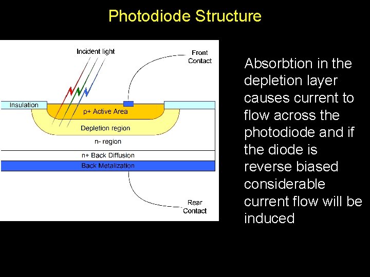
Photodiode Structure Absorbtion in the depletion layer causes current to flow across the photodiode and if the diode is reverse biased considerable current flow will be induced

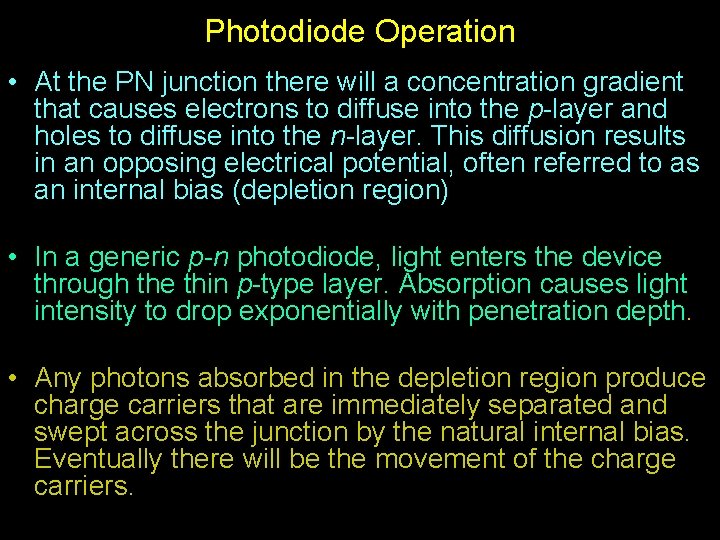
Photodiode Operation • At the PN junction there will a concentration gradient that causes electrons to diffuse into the p-layer and holes to diffuse into the n-layer. This diffusion results in an opposing electrical potential, often referred to as an internal bias (depletion region) • In a generic p-n photodiode, light enters the device through the thin p-type layer. Absorption causes light intensity to drop exponentially with penetration depth. • Any photons absorbed in the depletion region produce charge carriers that are immediately separated and swept across the junction by the natural internal bias. Eventually there will be the movement of the charge carriers.

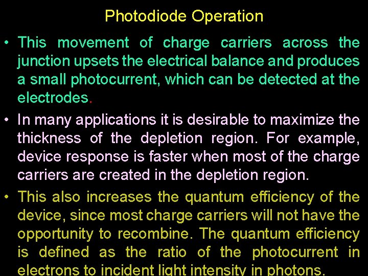
Photodiode Operation • This movement of charge carriers across the junction upsets the electrical balance and produces a small photocurrent, which can be detected at the electrodes. • In many applications it is desirable to maximize thickness of the depletion region. For example, device response is faster when most of the charge carriers are created in the depletion region. • This also increases the quantum efficiency of the device, since most charge carriers will not have the opportunity to recombine. The quantum efficiency is defined as the ratio of the photocurrent in electrons to incident light intensity in photons.

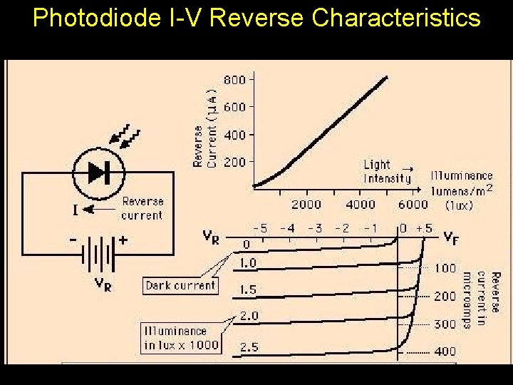
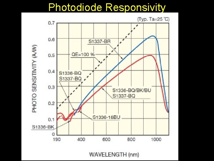
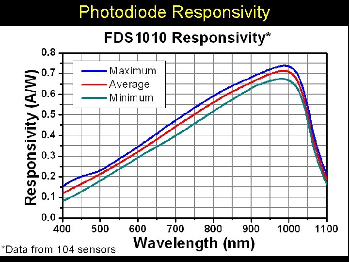
Photodiode Parameters • Responsivity: • The Spectral responsivity is a ratio of the generated photocurrent to incident light power, expressed in A/W when used in photoconductive mode. • Dark Current: The current through the photodiode in the absence of light, when it is operated in photoconductive mode.

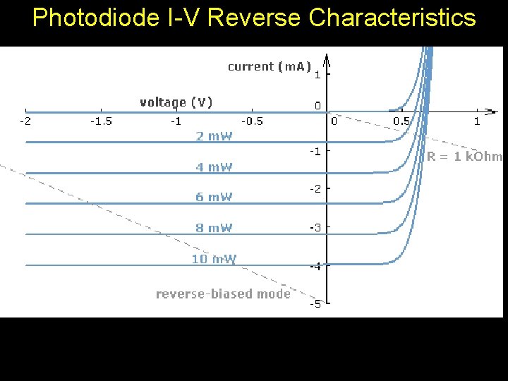
Photodiode I-V Reverse Characteristics

Photodiode I-V Reverse Characteristics

Photodiode Responsivity

Photodiode Responsivity

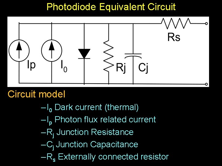
Photodiode Equivalent Circuit model – I 0 Dark current (thermal) – Ip Photon flux related current – Rj Junction Resistance – Cj Junction Capacitance – Rs Externally connected resistor

Photodiode Connected to an Operational; Amplifier • Current to voltage converter (amplifier

Photodiode Applications • Photodiodes are used in consumer electronics devices such as CD players, smoke detectors, and the receivers for infrared remote control devices used to control equipment from televisions to air conditioners. • Photodiodes are used as a light sensors. • Photodiodes are often used for accurate measurement of light intensity in science and industry. • They are also widely used in various medical applications, such as detectors for computer tomography, instruments to analyze samples, and pulse oximeters.

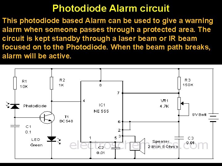
Photodiode Alarm circuit This photodiode based Alarm can be used to give a warning alarm when someone passes through a protected area. The circuit is kept standby through a laser beam or IR beam focused on to the Photodiode. When the beam path breaks, alarm will be active.