Shri Sant Gajanan Maharaj College of Engineering Department

- Slides: 39

Shri Sant Gajanan Maharaj College of Engineering Department of Electronics & Telecommunications Engineering Electronic Devices & Components Unit – IV Ordinary Diode & Zener Diode PN Junction Diode Characteristics

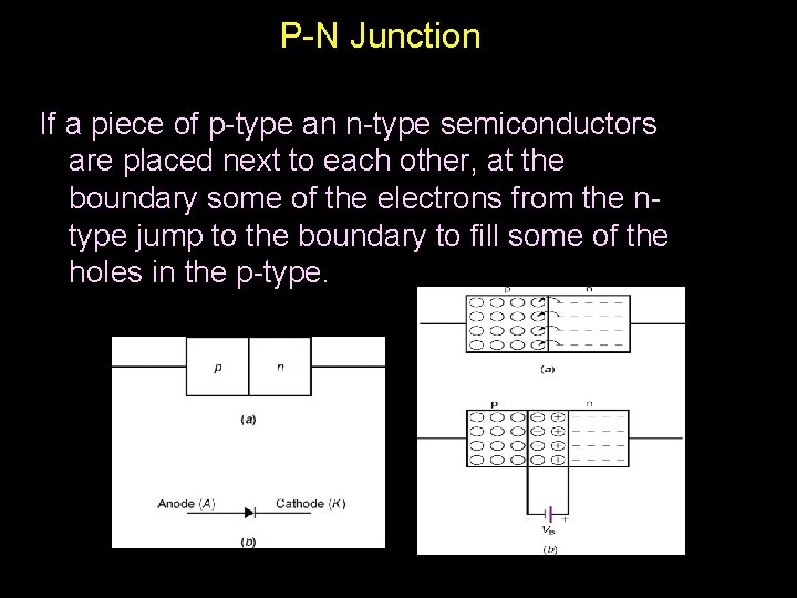
P-N Junction If a piece of p-type an n-type semiconductors are placed next to each other, at the boundary some of the electrons from the ntype jump to the boundary to fill some of the holes in the p-type.

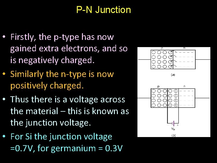
P-N Junction • Firstly, the p-type has now gained extra electrons, and so is negatively charged. • Similarly the n-type is now positively charged. • Thus there is a voltage across the material – this is known as the junction voltage. • For Si the junction voltage =0. 7 V, for germanium = 0. 3 V

Depletion Layer • Also, at the boundary region (junction) there are no free electrons and no holes (as they have cancelled each other) • Thus, in this region there are no free charge carriers, so no conduction can occur. This insulating layer is called the depletion layer

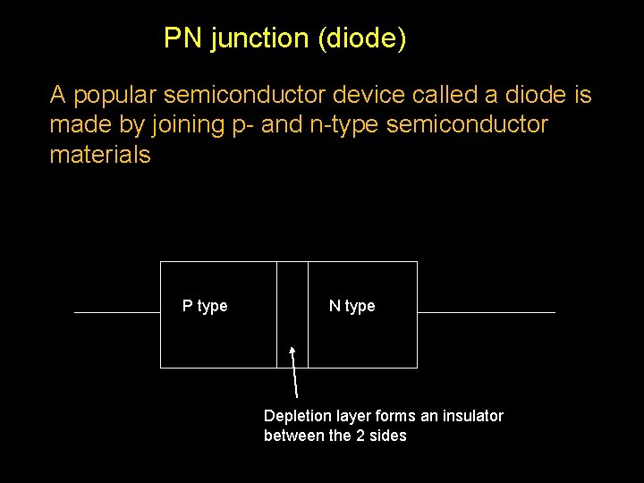
PN junction (diode) A popular semiconductor device called a diode is made by joining p- and n-type semiconductor materials P type N type Depletion layer forms an insulator between the 2 sides

PN junction (diode) In order to get current to flow through the diode it is necessary to break down the depletion layer (i. e. drive free electrons and free holes into the layer)

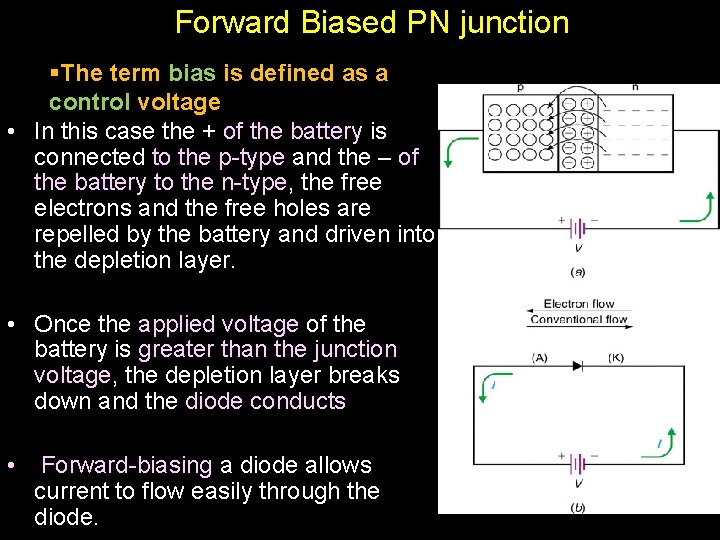
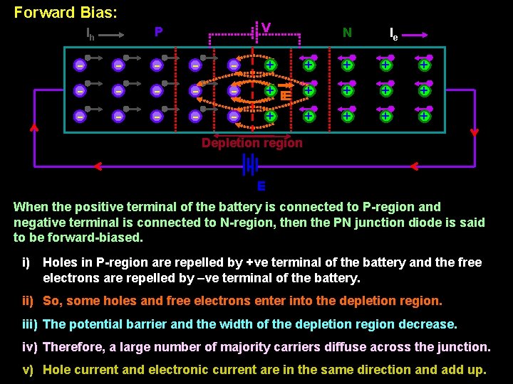
Forward Biased PN junction §The term bias is defined as a control voltage • In this case the + of the battery is connected to the p-type and the – of the battery to the n-type, the free electrons and the free holes are repelled by the battery and driven into the depletion layer. • Once the applied voltage of the battery is greater than the junction voltage, the depletion layer breaks down and the diode conducts • Forward-biasing a diode allows current to flow easily through the diode.

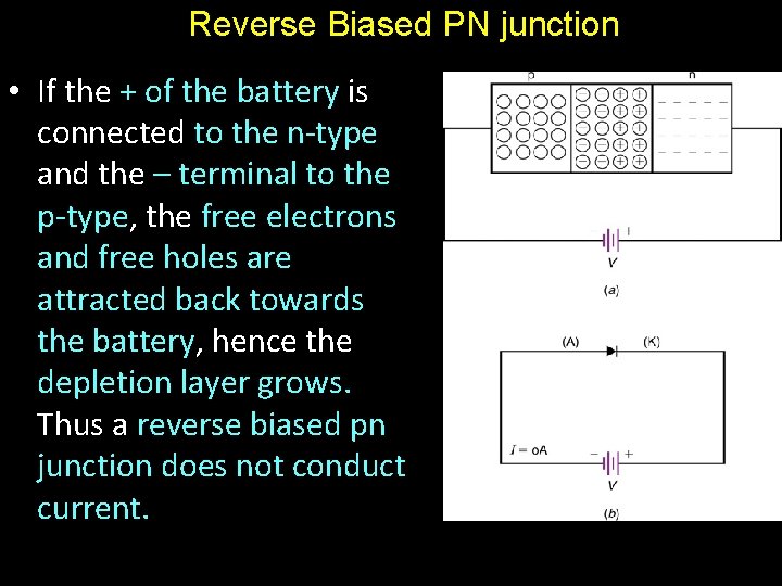
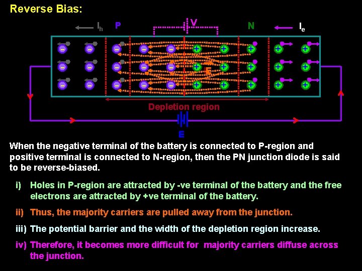
Reverse Biased PN junction • If the + of the battery is connected to the n-type and the – terminal to the p-type, the free electrons and free holes are attracted back towards the battery, hence the depletion layer grows. Thus a reverse biased pn junction does not conduct current.

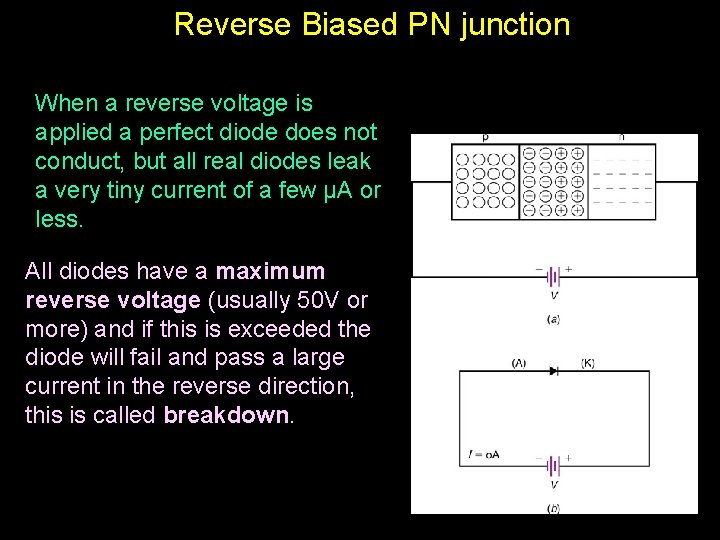
Reverse Biased PN junction When a reverse voltage is applied a perfect diode does not conduct, but all real diodes leak a very tiny current of a few µA or less. All diodes have a maximum reverse voltage (usually 50 V or more) and if this is exceeded the diode will fail and pass a large current in the reverse direction, this is called breakdown.

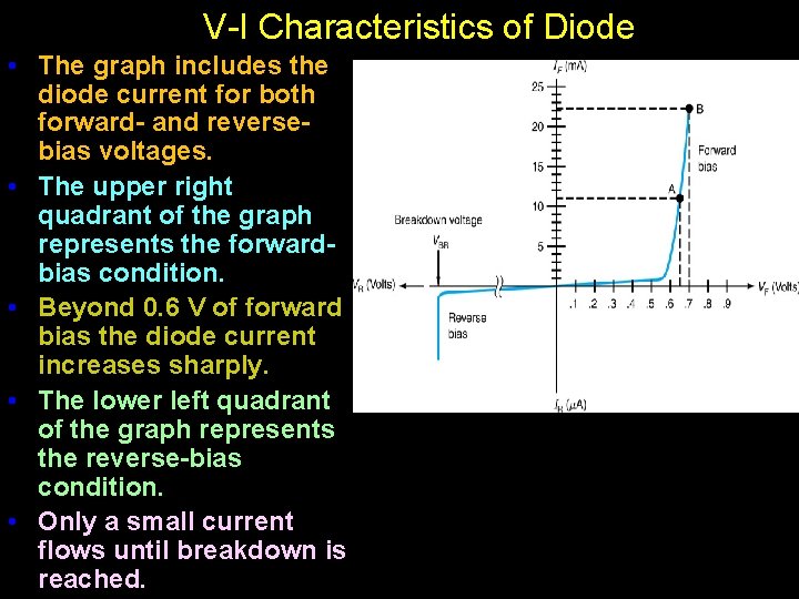
V-I Characteristics of Diode • The graph includes the diode current for both forward- and reversebias voltages. • The upper right quadrant of the graph represents the forwardbias condition. • Beyond 0. 6 V of forward bias the diode current increases sharply. • The lower left quadrant of the graph represents the reverse-bias condition. • Only a small current flows until breakdown is reached.

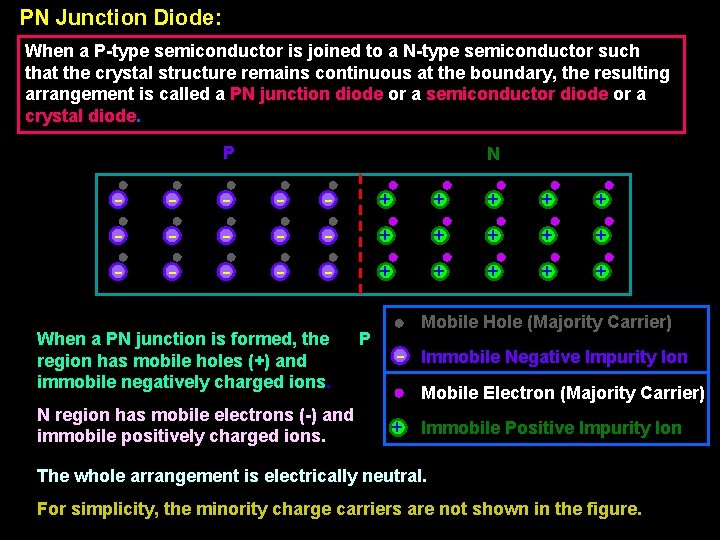
PN Junction Diode: When a P-type semiconductor is joined to a N-type semiconductor such that the crystal structure remains continuous at the boundary, the resulting arrangement is called a PN junction diode or a semiconductor diode or a crystal diode. P N - - - + + + + + - - - + + + When a PN junction is formed, the region has mobile holes (+) and immobile negatively charged ions. N region has mobile electrons (-) and immobile positively charged ions. P Mobile Hole (Majority Carrier) - Immobile Negative Impurity Ion Mobile Electron (Majority Carrier) + Immobile Positive Impurity Ion The whole arrangement is electrically neutral. For simplicity, the minority charge carriers are not shown in the figure.

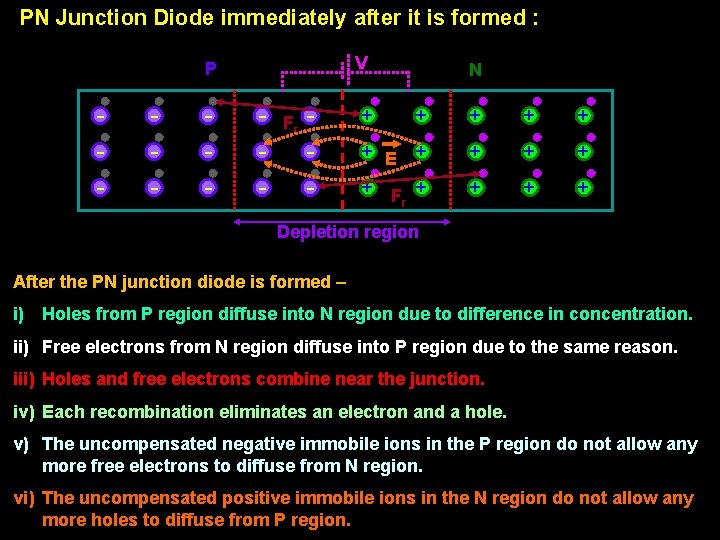
PN Junction Diode immediately after it is formed : V P - - Fr - N + + + E + + F + + + + r Depletion region After the PN junction diode is formed – i) Holes from P region diffuse into N region due to difference in concentration. ii) Free electrons from N region diffuse into P region due to the same reason. iii) Holes and free electrons combine near the junction. iv) Each recombination eliminates an electron and a hole. v) The uncompensated negative immobile ions in the P region do not allow any more free electrons to diffuse from N region. vi) The uncompensated positive immobile ions in the N region do not allow any more holes to diffuse from P region.

vii) The positive donor ions in the N region and the negative acceptor ions in the P region are left uncompensated. viii) The region containing the uncompensated acceptor and donor ions is called ‘depletion region’ because this region is devoid of mobile charges. Since the region is having only immobile charges, therefore, this region is also called ‘space charge region’. ix) The N region is having higher potential than P region. x) So, an electric field is set up as shown in the figure. xi) The difference in potential between P and N regions across the junction makes it difficult for the holes and electrons to move across the junction. This acts as a barrier and hence called ‘potential barrier’ or ‘height of the barrier’. xii) The physical distance between one side and the other side of the barrier is called ‘width of the barrier’. xiii) Potential barrier for Si is nearly 0. 7 V and for Ge is 0. 3 V. xiv) The potential barrier opposes the motion of the majority carriers. xv) However, a few majority carriers with high kinetic energy manage to overcome the barrier and cross the junction. ix) Potential barrier helps the movement of minority carriers.

Forward Bias: - V P Ih - - + N Ie + + + EE + + + + + Depletion region E When the positive terminal of the battery is connected to P-region and negative terminal is connected to N-region, then the PN junction diode is said to be forward-biased. i) Holes in P-region are repelled by +ve terminal of the battery and the free electrons are repelled by –ve terminal of the battery. ii) So, some holes and free electrons enter into the depletion region. iii) The potential barrier and the width of the depletion region decrease. iv) Therefore, a large number of majority carriers diffuse across the junction. v) Hole current and electronic current are in the same direction and add up.

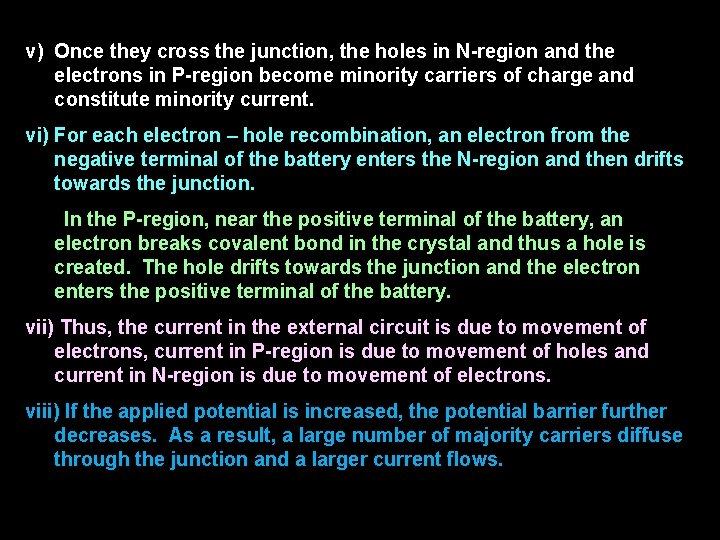
v) Once they cross the junction, the holes in N-region and the electrons in P-region become minority carriers of charge and constitute minority current. vi) For each electron – hole recombination, an electron from the negative terminal of the battery enters the N-region and then drifts towards the junction. In the P-region, near the positive terminal of the battery, an electron breaks covalent bond in the crystal and thus a hole is created. The hole drifts towards the junction and the electron enters the positive terminal of the battery. vii) Thus, the current in the external circuit is due to movement of electrons, current in P-region is due to movement of holes and current in N-region is due to movement of electrons. viii) If the applied potential is increased, the potential barrier further decreases. As a result, a large number of majority carriers diffuse through the junction and a larger current flows.

Reverse Bias: Ih V P - - - - - + N Ie + + + EE + + + + + Depletion region E When the negative terminal of the battery is connected to P-region and positive terminal is connected to N-region, then the PN junction diode is said to be reverse-biased. i) Holes in P-region are attracted by -ve terminal of the battery and the free electrons are attracted by +ve terminal of the battery. ii) Thus, the majority carriers are pulled away from the junction. iii) The potential barrier and the width of the depletion region increase. iv) Therefore, it becomes more difficult for majority carriers diffuse across the junction.

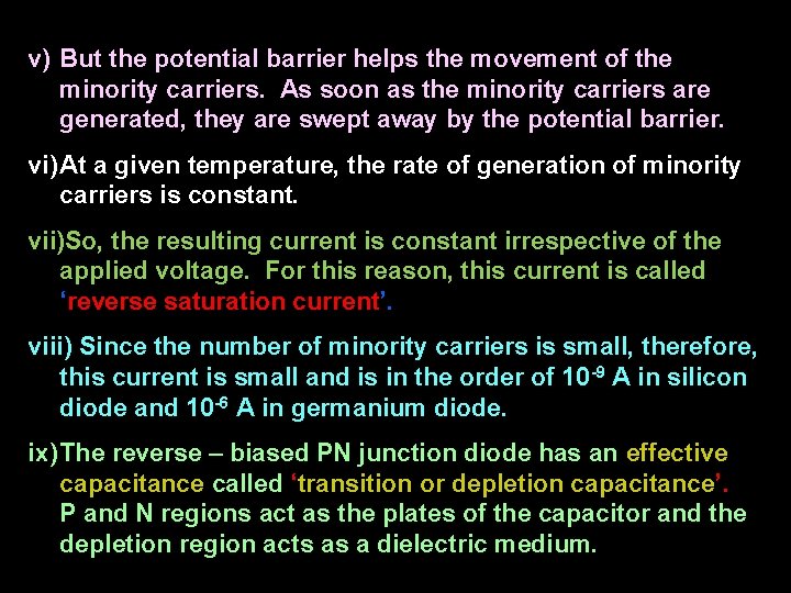
v) But the potential barrier helps the movement of the minority carriers. As soon as the minority carriers are generated, they are swept away by the potential barrier. vi) At a given temperature, the rate of generation of minority carriers is constant. vii)So, the resulting current is constant irrespective of the applied voltage. For this reason, this current is called ‘reverse saturation current’. viii) Since the number of minority carriers is small, therefore, this current is small and is in the order of 10 -9 A in silicon diode and 10 -6 A in germanium diode. ix) The reverse – biased PN junction diode has an effective capacitance called ‘transition or depletion capacitance’. P and N regions act as the plates of the capacitor and the depletion region acts as a dielectric medium.

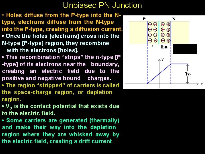
Unbiased PN Junction • Holes diffuse from the P-type into the Ntype, electrons diffuse from the N-type into the P-type, creating a diffusion current. • Once the holes [electrons] cross into the N-type [P-type] region, they recombine with the electrons [holes]. • This recombination “strips” the n-type [P -type] of its electrons near the boundary, creating an electric field due to the positive and negative bound charges. • The region “stripped” of carriers is called the space-charge region, or depletion region. • V 0 is the contact potential that exists due to the electric field. • Some carriers are generated (thermally) and make their way into the depletion region where they are whisked away by the electric field, creating a drift current.

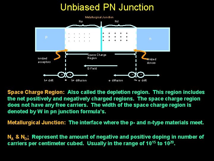
Unbiased PN Junction Metallurgical Junction Na - P - - Nd - - + + + + + n Space Charge Region ionized acceptors ionized donors E-Field + h+ drift _ + = = h+ diffusion e- diffusion _ == e- drift Space Charge Region: Also called the depletion region. This region includes the net positively and negatively charged regions. The space charge region does not have any free carriers. The width of the space charge region is denoted by W in pn junction formula’s. Metallurgical Junction: The interface where the p- and n-type materials meet. NA & ND: Represent the amount of negative and positive doping in number of carriers per centimeter cubed. Usually in the range of 1015 to 1020.

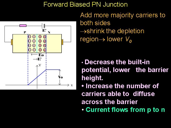
Forward Biased PN Junction Add more majority carriers to both sides shrink the depletion region lower V 0 • Decrease the built-in potential, lower the barrier height. • Increase the number of carriers able to diffuse across the barrier • Current flows from p to n

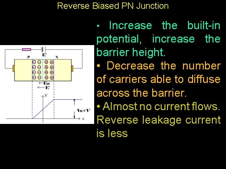
Reverse Biased PN Junction • Increase the built-in potential, increase the barrier height. • Decrease the number of carriers able to diffuse across the barrier. • Almost no current flows. Reverse leakage current is less

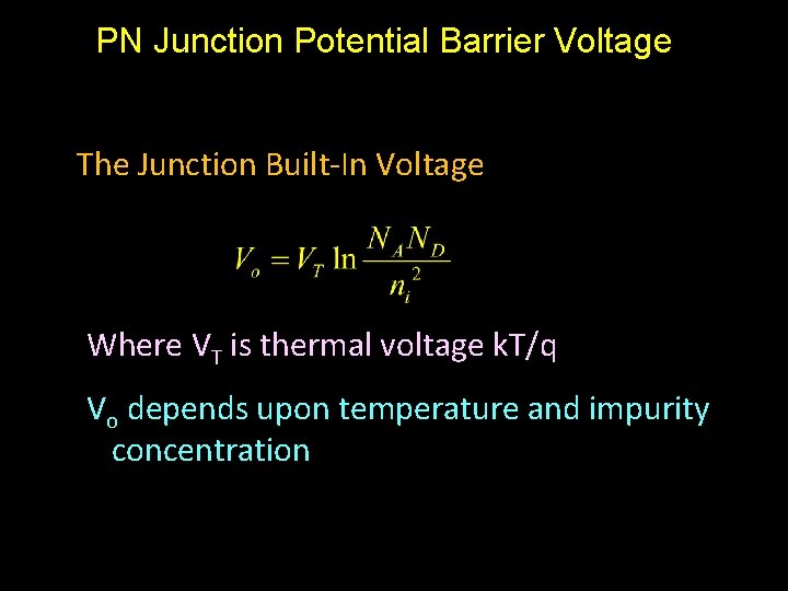
PN Junction Potential Barrier Voltage The Junction Built-In Voltage Where VT is thermal voltage k. T/q Vo depends upon temperature and impurity concentration

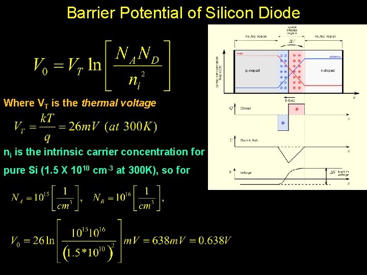
Barrier Potential of Silicon Diode Where VT is thermal voltage ni is the intrinsic carrier concentration for pure Si (1. 5 X 1010 cm-3 at 300 K), so for

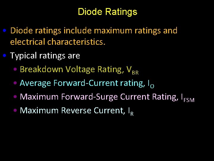
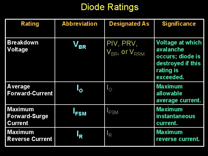
Diode Ratings • Diode ratings include maximum ratings and electrical characteristics. • Typical ratings are • Breakdown Voltage Rating, VBR • Average Forward-Current rating, IO • Maximum Forward-Surge Current Rating, IFSM • Maximum Reverse Current, IR

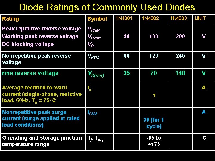
Diode Ratings of Commonly Used Diodes 1 N 4001 1 N 4002 1 N 4003 UNIT Rating Symbol Peak repetitive reverse voltage Working peak reverse voltage DC blocking voltage VRRM VRWM VR 50 100 200 V Nonrepetitive peak reverse voltage VRSM 60 120 240 V rms reverse voltage VR(rms) 35 70 140 V Average rectified forward current (single-phase, resistive load, 60 Hz, TA = 75 o. C Io Nonrepetitive peak surge current (surge applied at rated load conditions) IFSM Operating and storage junction temperature range Tj, Tstg A 1 A 30 (for 1 cycle) -65 to +175 o. C

Diode Ratings Rating Breakdown Voltage Average Forward-Current Maximum Forward-Surge Current Maximum Reverse Current Abbreviation VBR IO IFSM IR Designated As Significance PIV, PRV, VBR, or VRRM Voltage at which avalanche occurs; diode is destroyed if this rating is exceeded. IO Maximum allowable average current. IFSM Maximum instantaneous current. IR Maximum reverse current.

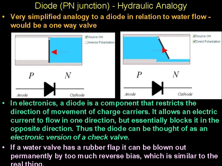
Diode (PN junction) - Hydraulic Analogy • Very simplified analogy to a diode in relation to water flow would be a one way valve • In electronics, a diode is a component that restricts the direction of movement of charge carriers. It allows an electric current to flow in one direction, but essentially blocks it in the opposite direction. Thus the diode can be thought of as an electronic version of a check valve. • If a water valve has a rubber flap it can be blown out permanently by too much reverse bias, which is similar to the

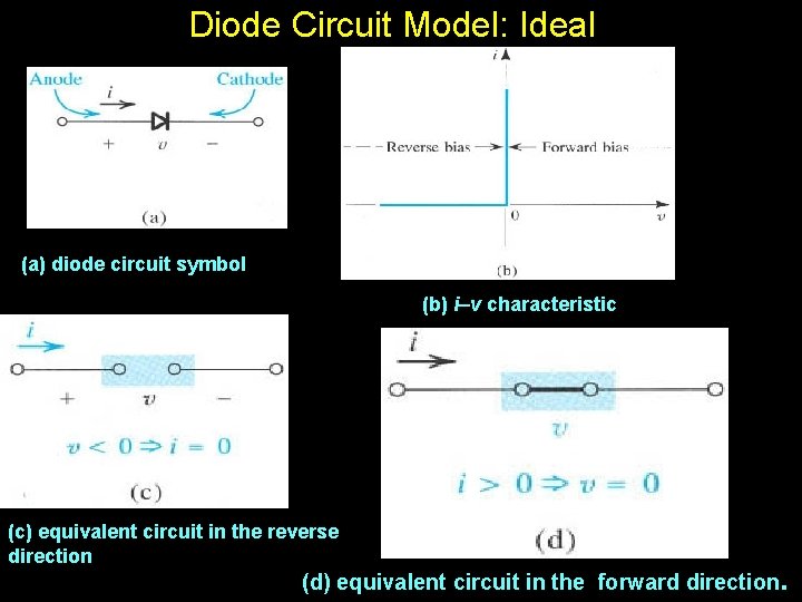
Diode Circuit Model: Ideal (a) diode circuit symbol (b) i–v characteristic (c) equivalent circuit in the reverse direction (d) equivalent circuit in the forward direction .

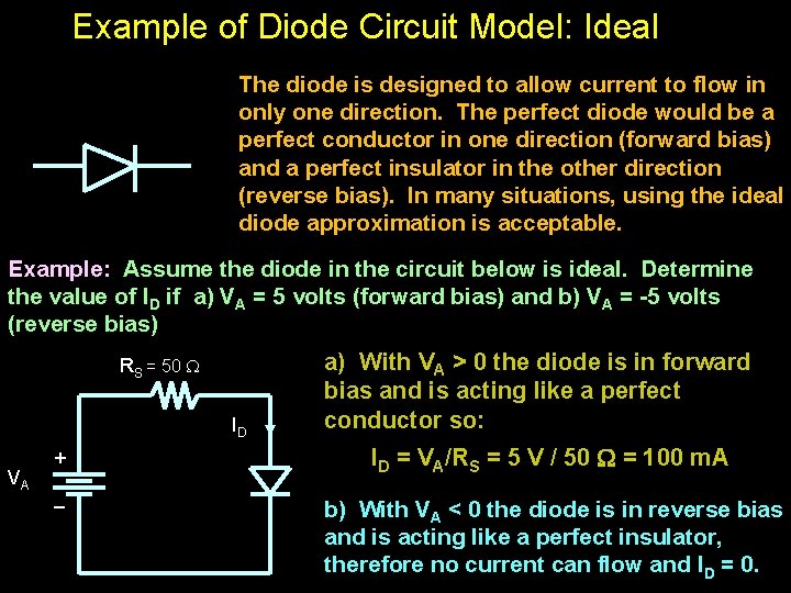
Example of Diode Circuit Model: Ideal The diode is designed to allow current to flow in only one direction. The perfect diode would be a perfect conductor in one direction (forward bias) and a perfect insulator in the other direction (reverse bias). In many situations, using the ideal diode approximation is acceptable. Example: Assume the diode in the circuit below is ideal. Determine the value of ID if a) VA = 5 volts (forward bias) and b) VA = -5 volts (reverse bias) RS = 50 ID VA + _ a) With VA > 0 the diode is in forward bias and is acting like a perfect conductor so: ID = VA/RS = 5 V / 50 = 100 m. A b) With VA < 0 the diode is in reverse bias and is acting like a perfect insulator, therefore no current can flow and ID = 0.

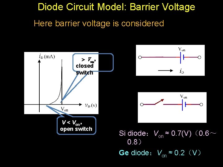
Diode Circuit Model: Barrier Voltage Here barrier voltage is considered V Von, closed switch V < Von, open switch Si diode:Von ≈ 0. 7(V)(0. 6~ 0. 8) Ge diode:Von ≈ 0. 2(V)

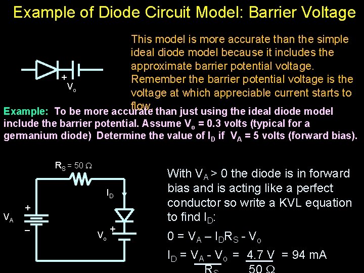
Example of Diode Circuit Model: Barrier Voltage This model is more accurate than the simple ideal diode model because it includes the approximate barrier potential voltage. + Remember the barrier potential voltage is the Vo voltage at which appreciable current starts to flow. Example: To be more accurate than just using the ideal diode model include the barrier potential. Assume Vo = 0. 3 volts (typical for a germanium diode) Determine the value of ID if VA = 5 volts (forward bias). RS = 50 ID VA + _ Vo + With VA > 0 the diode is in forward bias and is acting like a perfect conductor so write a KVL equation to find ID: 0 = V A – I DR S - V o ID = VA - Vo = 4. 7 V = 94 m. A

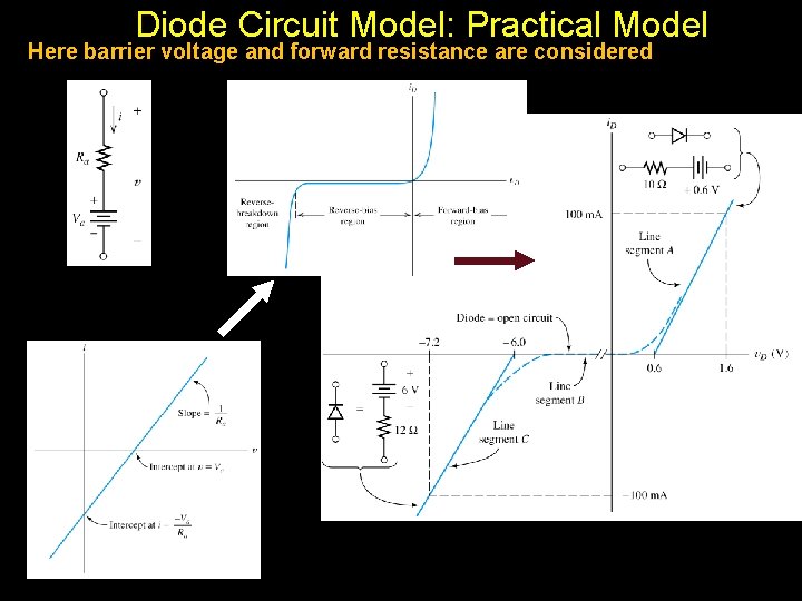
Diode Circuit Model: Practical Model Here barrier voltage and forward resistance are considered

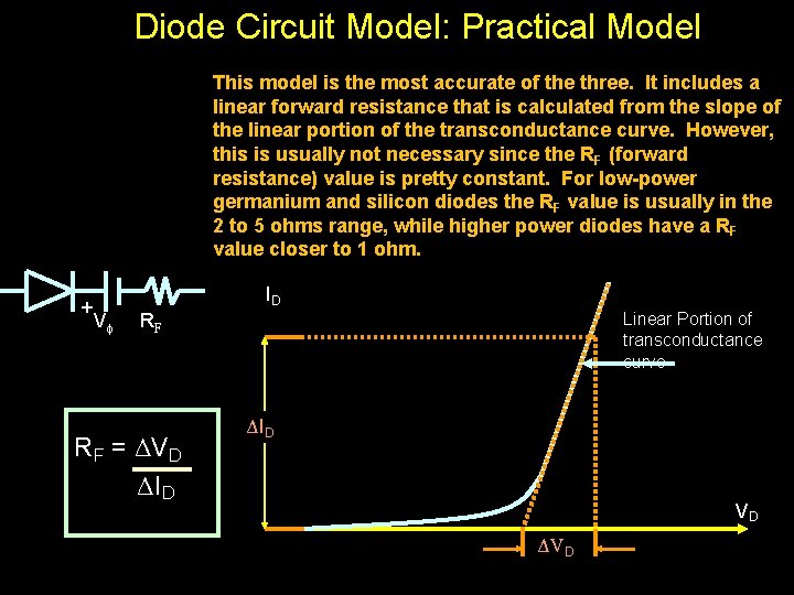
Diode Circuit Model: Practical Model This model is the most accurate of the three. It includes a linear forward resistance that is calculated from the slope of the linear portion of the transconductance curve. However, this is usually not necessary since the RF (forward resistance) value is pretty constant. For low-power germanium and silicon diodes the RF value is usually in the 2 to 5 ohms range, while higher power diodes have a R F value closer to 1 ohm. + ID V Linear Portion of transconductance curve RF R F = ΔV D ΔI D VD ΔV D

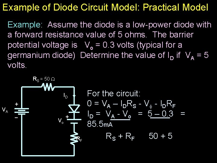
Example of Diode Circuit Model: Practical Model Example: Assume the diode is a low-power diode with a forward resistance value of 5 ohms. The barrier potential voltage is Vo = 0. 3 volts (typical for a germanium diode) Determine the value of ID if VA = 5 volts. RS = 50 ID VA + _ Vo + RF For the circuit: 0 = V A – I DR S - V - I DR F ID = VA - Vo = 5 – 0. 3 = 85. 5 m. A RS + R F 50 + 5

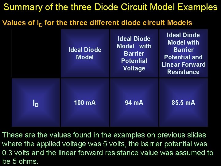
Summary of the three Diode Circuit Model Examples Values of ID for the three different diode circuit Models ID Ideal Diode Model with Barrier Potential Voltage Ideal Diode Model with Barrier Potential and Linear Forward Resistance 100 m. A 94 m. A 85. 5 m. A These are the values found in the examples on previous slides where the applied voltage was 5 volts, the barrier potential was 0. 3 volts and the linear forward resistance value was assumed to be 5 ohms.

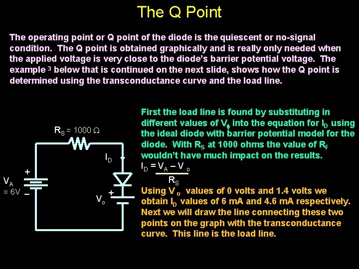
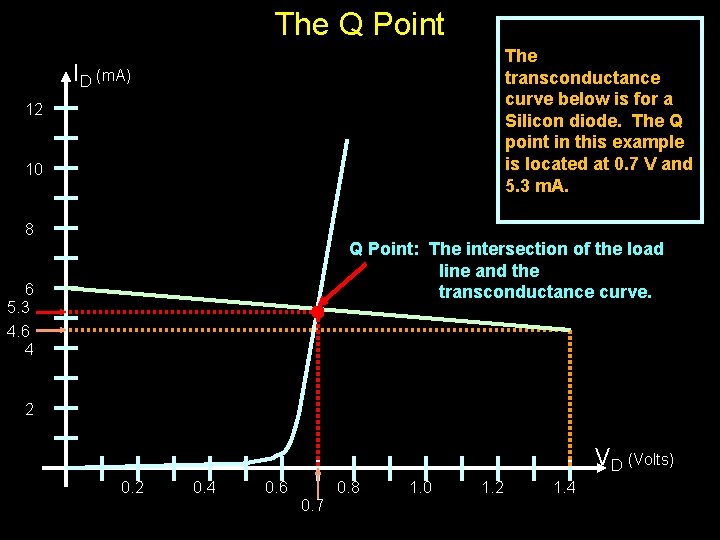
The Q Point The operating point or Q point of the diode is the quiescent or no-signal condition. The Q point is obtained graphically and is really only needed when the applied voltage is very close to the diode’s barrier potential voltage. The example 3 below that is continued on the next slide, shows how the Q point is determined using the transconductance curve and the load line. RS = 1000 ID VA + = 6 V _ Vo + First the load line is found by substituting in different values of V into the equation for ID using the ideal diode with barrier potential model for the diode. With RS at 1000 ohms the value of RF wouldn’t have much impact on the results. ID = V A – V o RS Using V o values of 0 volts and 1. 4 volts we obtain ID values of 6 m. A and 4. 6 m. A respectively. Next we will draw the line connecting these two points on the graph with the transconductance curve. This line is the load line.

The Q Point The transconductance curve below is for a Silicon diode. The Q point in this example is located at 0. 7 V and 5. 3 m. A. ID (m. A) 12 10 8 Q Point: The intersection of the load line and the transconductance curve. 6 5. 3 4. 6 4 2 VD (Volts) 0. 2 0. 4 0. 6 0. 7 0. 8 1. 0 1. 2 1. 4

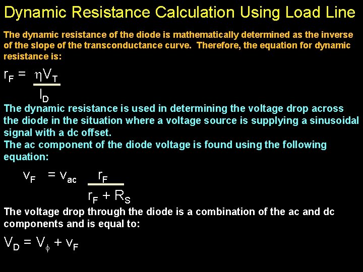
Dynamic Resistance Calculation Using Load Line The dynamic resistance of the diode is mathematically determined as the inverse of the slope of the transconductance curve. Therefore, the equation for dynamic resistance is: r. F = V T ID The dynamic resistance is used in determining the voltage drop across the diode in the situation where a voltage source is supplying a sinusoidal signal with a dc offset. The ac component of the diode voltage is found using the following equation: v. F = vac r. F + RS The voltage drop through the diode is a combination of the ac and dc components and is equal to: VD = V + v F

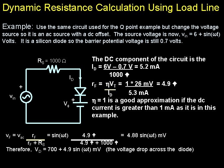
Dynamic Resistance Calculation Using Load Line Example: Use the same circuit used for the Q point example but change the voltage source so it is an ac source with a dc offset. The source voltage is now, vin = 6 + sin(ωt) Volts. It is a silicon diode so the barrier potential voltage is still 0. 7 volts. RS = 1000 ID + vin V v. F = vac + The DC component of the circuit is the ID = 6 V – 0. 7 V = 5. 2 m. A 1000 r. F = VT = 1 * 26 m. V = 4. 9 ID 5. 3 m. A = 1 is a good approximation if the dc current is greater than 1 m. A as it is in this example. r. F = sin(ωt) 4. 9 = 4. 88 sin(ωt) m. V r F + RS 4. 9 + 1000 Therefore, VD = 700 + 4. 9 sin (ωt) m. V (the voltage drop across the diode)