Shri Sant Gajanan Maharaj College of Engineering Department
![Application of PCB [Copper Clad Laminates] From schematic, PCB Layout is drawn and the Application of PCB [Copper Clad Laminates] From schematic, PCB Layout is drawn and the](https://slidetodoc.com/presentation_image/375979016e2f3e1c39caac83ed12a400/image-6.jpg)
![Application of PCB [Copper Clad Laminates] From schematic, PCB Layout is drawn and the Application of PCB [Copper Clad Laminates] From schematic, PCB Layout is drawn and the](https://slidetodoc.com/presentation_image/375979016e2f3e1c39caac83ed12a400/image-7.jpg)
![Application of PCB [Copper Clad Laminates] Drawing PCB Layout is an art. Some rules Application of PCB [Copper Clad Laminates] Drawing PCB Layout is an art. Some rules](https://slidetodoc.com/presentation_image/375979016e2f3e1c39caac83ed12a400/image-8.jpg)
![Application of PCB [Copper Clad Laminates] The layout may drawn by hand on trace Application of PCB [Copper Clad Laminates] The layout may drawn by hand on trace](https://slidetodoc.com/presentation_image/375979016e2f3e1c39caac83ed12a400/image-9.jpg)
![Application of PCB [Copper Clad Laminates] The layout may drawn by hand on trace Application of PCB [Copper Clad Laminates] The layout may drawn by hand on trace](https://slidetodoc.com/presentation_image/375979016e2f3e1c39caac83ed12a400/image-10.jpg)
![Application of PCB [Copper Clad Laminates] The solder side and Component side are shown. Application of PCB [Copper Clad Laminates] The solder side and Component side are shown.](https://slidetodoc.com/presentation_image/375979016e2f3e1c39caac83ed12a400/image-11.jpg)
![Traces [copper tracks] • Traces connect pads together. • Traces are essentially the wiring Traces [copper tracks] • Traces connect pads together. • Traces are essentially the wiring](https://slidetodoc.com/presentation_image/375979016e2f3e1c39caac83ed12a400/image-30.jpg)
- Slides: 36

Shri Sant Gajanan Maharaj College of Engineering Department of Electronics & Telecommunications Engineering Electronic Devices & Components Unit – III Printed Circuit Boards Manufacture, Development and Soldering Techniques Introduction to PCB and its Parts

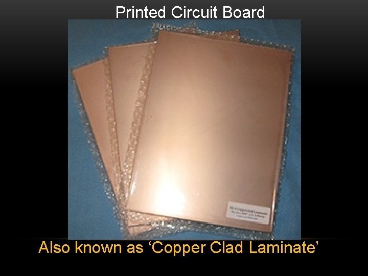
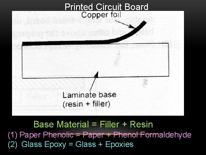
Printed Circuit Board Also known as ‘Copper Clad Laminate’

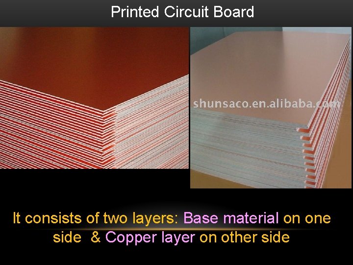
Printed Circuit Board It consists of two layers: Base material on one side & Copper layer on other side

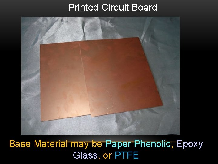
Printed Circuit Board Base Material may be Paper Phenolic, Epoxy Glass, or PTFE

Printed Circuit Board Base Material = Filler + Resin (1) Paper Phenolic = Paper + Phenol Formaldehyde (2) Glass Epoxy = Glass + Epoxies
![Application of PCB Copper Clad Laminates From schematic PCB Layout is drawn and the Application of PCB [Copper Clad Laminates] From schematic, PCB Layout is drawn and the](https://slidetodoc.com/presentation_image/375979016e2f3e1c39caac83ed12a400/image-6.jpg)
Application of PCB [Copper Clad Laminates] From schematic, PCB Layout is drawn and the pattern is then transferred on the PCB
![Application of PCB Copper Clad Laminates From schematic PCB Layout is drawn and the Application of PCB [Copper Clad Laminates] From schematic, PCB Layout is drawn and the](https://slidetodoc.com/presentation_image/375979016e2f3e1c39caac83ed12a400/image-7.jpg)
Application of PCB [Copper Clad Laminates] From schematic, PCB Layout is drawn and the pattern is then transferred on the PCB
![Application of PCB Copper Clad Laminates Drawing PCB Layout is an art Some rules Application of PCB [Copper Clad Laminates] Drawing PCB Layout is an art. Some rules](https://slidetodoc.com/presentation_image/375979016e2f3e1c39caac83ed12a400/image-8.jpg)
Application of PCB [Copper Clad Laminates] Drawing PCB Layout is an art. Some rules are laid down for efficient layout drawing
![Application of PCB Copper Clad Laminates The layout may drawn by hand on trace Application of PCB [Copper Clad Laminates] The layout may drawn by hand on trace](https://slidetodoc.com/presentation_image/375979016e2f3e1c39caac83ed12a400/image-9.jpg)
Application of PCB [Copper Clad Laminates] The layout may drawn by hand on trace paper or through software like Express. PCB, Dip. Trace, Eagle, Ultiboard
![Application of PCB Copper Clad Laminates The layout may drawn by hand on trace Application of PCB [Copper Clad Laminates] The layout may drawn by hand on trace](https://slidetodoc.com/presentation_image/375979016e2f3e1c39caac83ed12a400/image-10.jpg)
Application of PCB [Copper Clad Laminates] The layout may drawn by hand on trace paper or through software like Express. PCB, Dip. Trace, Eagle, Ultiboard
![Application of PCB Copper Clad Laminates The solder side and Component side are shown Application of PCB [Copper Clad Laminates] The solder side and Component side are shown.](https://slidetodoc.com/presentation_image/375979016e2f3e1c39caac83ed12a400/image-11.jpg)
Application of PCB [Copper Clad Laminates] The solder side and Component side are shown. IC sockets must be soldered and then ICs must be inserted in to them.

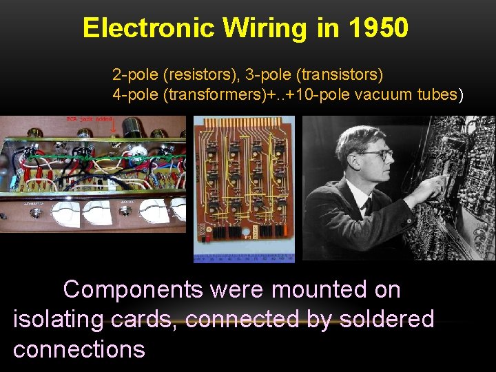
Electronic Wiring in 1950 2 -pole (resistors), 3 -pole (transistors) 4 -pole (transformers)+. . +10 -pole vacuum tubes) Components were mounted on isolating cards, connected by soldered connections

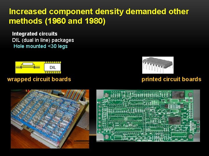
Increased component density demanded other methods (1960 and 1980) Integrated circuits DIL (dual in line) packages Hole mounted <30 legs wrapped circuit boards printed circuit boards

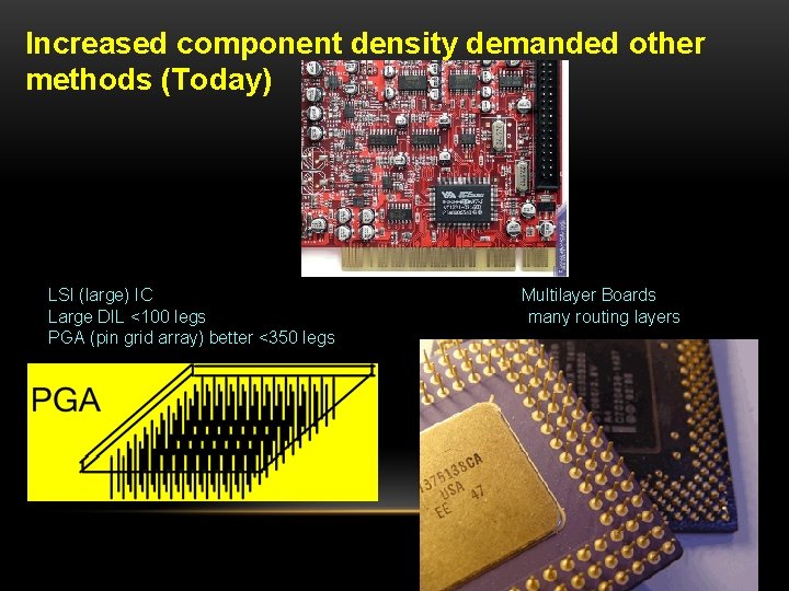
Increased component density demanded other methods (Today) LSI (large) IC Multilayer Boards Large DIL <100 legs many routing layers PGA (pin grid array) better <350 legs

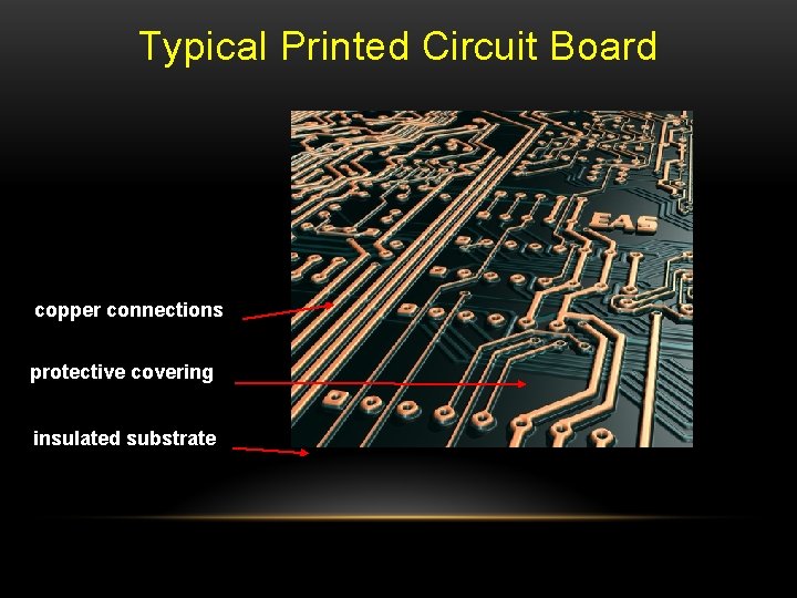
Typical Printed Circuit Board copper connections protective covering insulated substrate

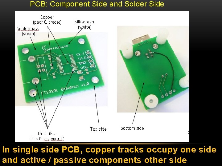
PCB: Component Side and Solder Side In single side PCB, copper tracks occupy one side and active / passive components other side

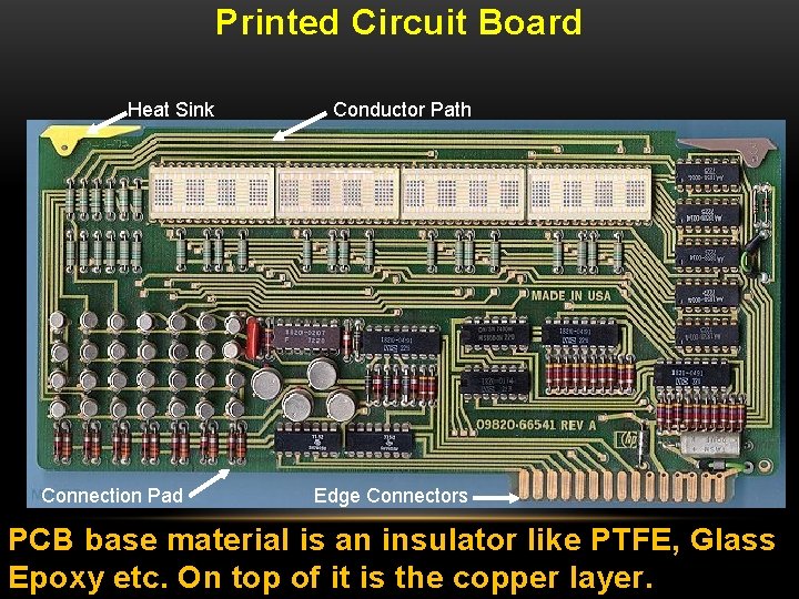
Printed Circuit Board Heat Sink Connection Pad Conductor Path Edge Connectors PCB base material is an insulator like PTFE, Glass Epoxy etc. On top of it is the copper layer.

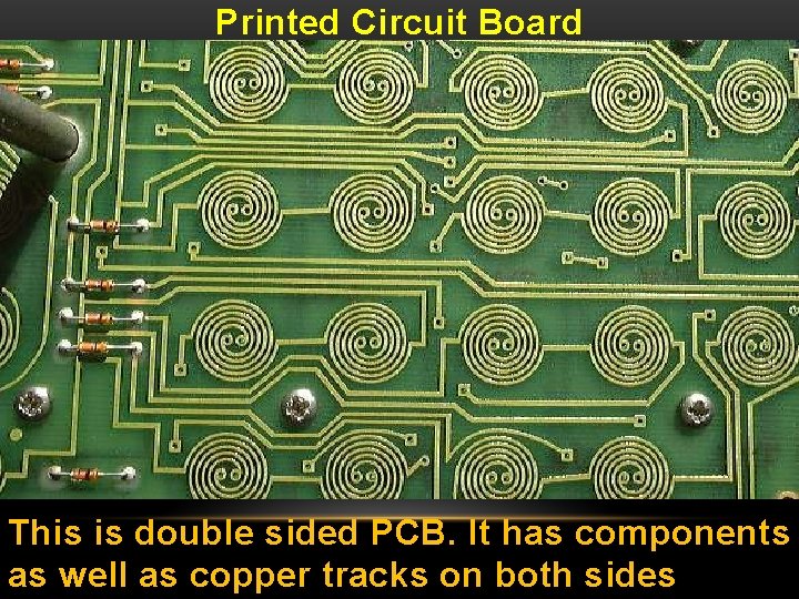
Printed Circuit Board This is double sided PCB. It has components as well as copper tracks on both sides

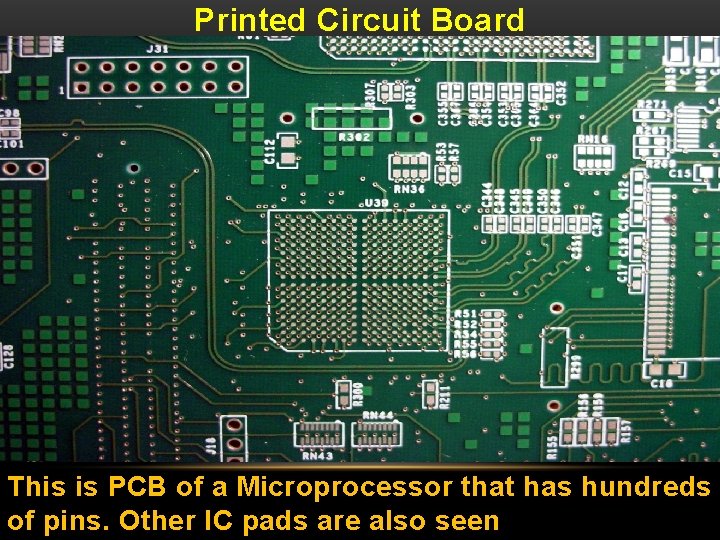
Printed Circuit Board This is PCB of a Microprocessor that has hundreds of pins. Other IC pads are also seen

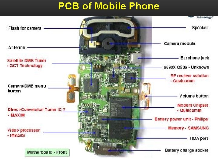
PCB of Mobile Phone

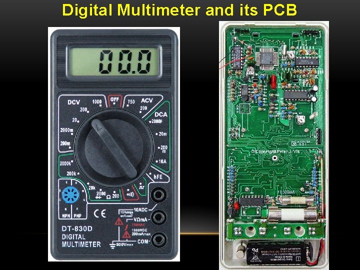
Digital Multimeter and its PCB

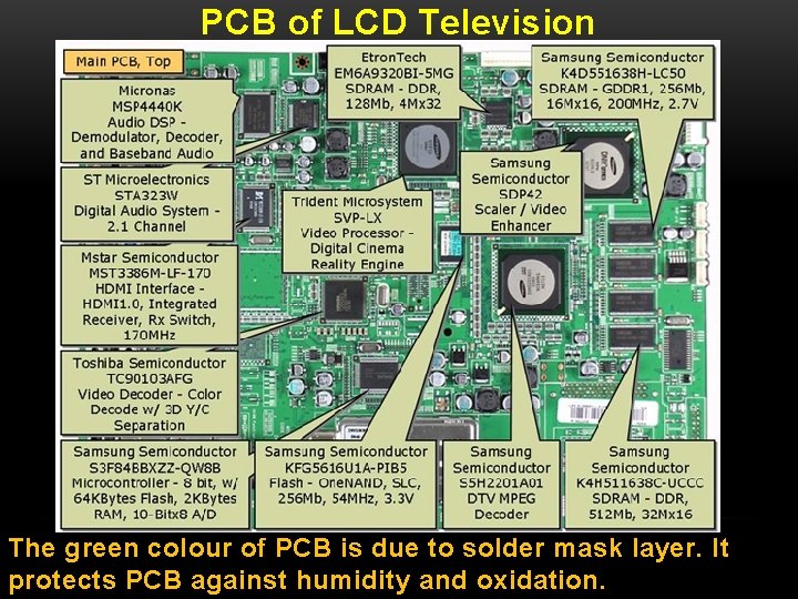
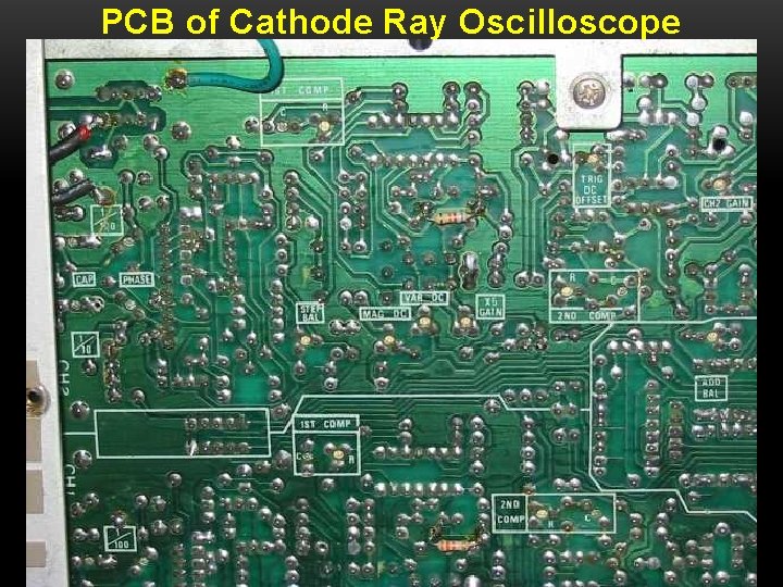
PCB of LCD Television The green colour of PCB is due to solder mask layer. It protects PCB against humidity and oxidation.

PCB of Cathode Ray Oscilloscope

Printed Circuit Board PCB means Copper Clad Laminate It has base material on which copper layer is deposited Base material can be PTFE, Epoxy Resin, Epoxy Glass, Silicon Resin, Paper Phenolic. These are insulators and they give solid support to copper layer

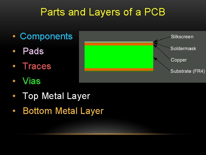
Parts of PCB • Conducting layers are typically made of thin copper foil. • The board is typically coated with a solder mask that is green in color. Other colors that are normally available are blue and red. • Unwanted copper is removed from the substrate after etching leaving only the desired copper traces or pathways

Parts of a PCB • Components • Pads • Traces • Vias • Top Metal Layer • Bottom Metal Layer

Parts and Layers of a PCB • Components • Pads • Traces • Vias • Top Metal Layer • Bottom Metal Layer

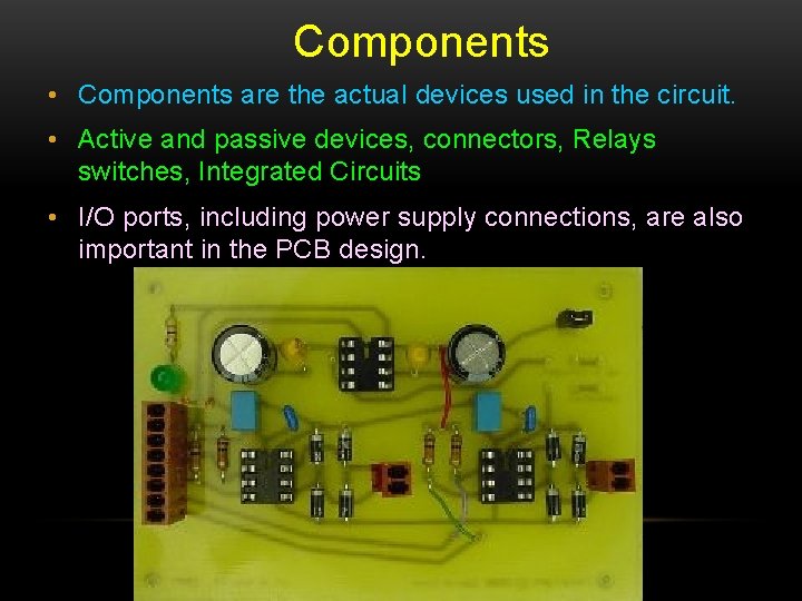
Components • Components are the actual devices used in the circuit. • Active and passive devices, connectors, Relays switches, Integrated Circuits • I/O ports, including power supply connections, are also important in the PCB design.

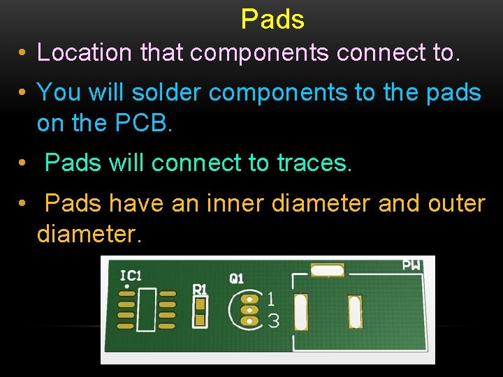
Pads • Location that components connect to. • You will solder components to the pads on the PCB. • Pads will connect to traces. • Pads have an inner diameter and outer diameter.
![Traces copper tracks Traces connect pads together Traces are essentially the wiring Traces [copper tracks] • Traces connect pads together. • Traces are essentially the wiring](https://slidetodoc.com/presentation_image/375979016e2f3e1c39caac83ed12a400/image-30.jpg)
Traces [copper tracks] • Traces connect pads together. • Traces are essentially the wiring of the PCB. • Equivalent to wire for conducting signals • Traces sometimes connect to vias [PTH] • High current traces should be wide. • Power supply and Ground traces are thicker than signal tracks

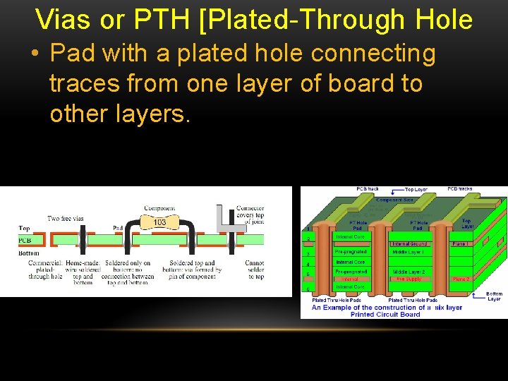
Vias or PTH [Plated-Through Hole • Pad with a plated hole connecting traces from one layer of board to other layers.

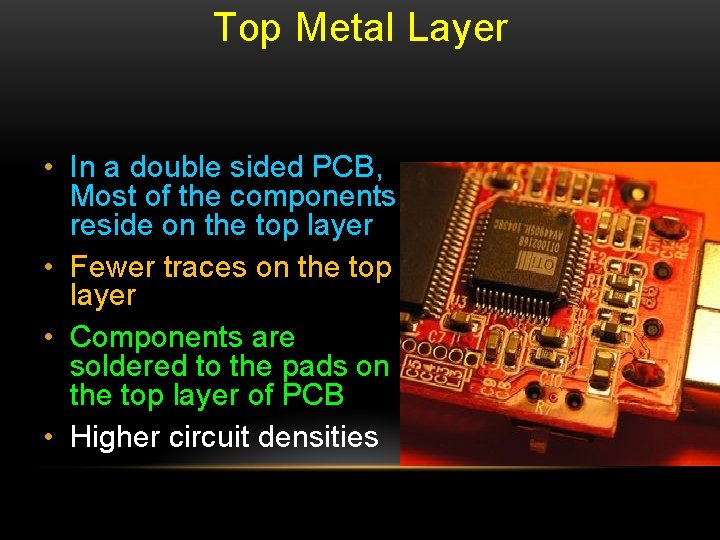
Top Metal Layer • In a double sided PCB, Most of the components reside on the top layer • Fewer traces on the top layer • Components are soldered to the pads on the top layer of PCB • Higher circuit densities

Bottom Metal Layer • Few components on this layer. • Many traces on this layer. • Most soldering done on this layer.

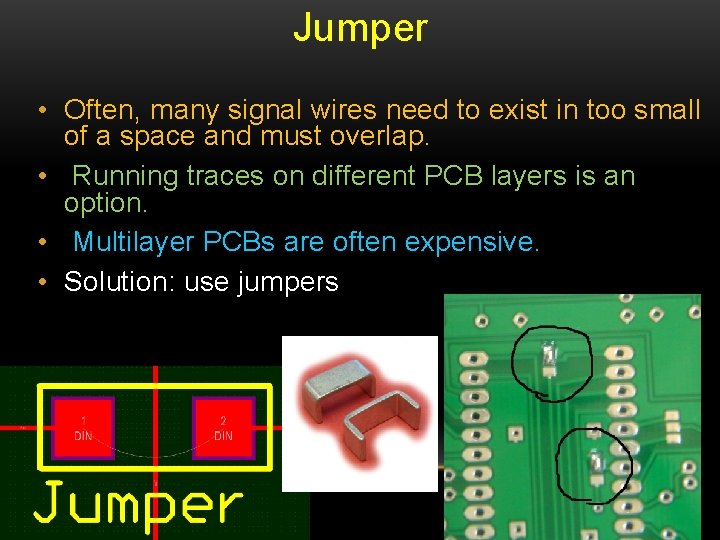
Jumper • Often, many signal wires need to exist in too small of a space and must overlap. • Running traces on different PCB layers is an option. • Multilayer PCBs are often expensive. • Solution: use jumpers

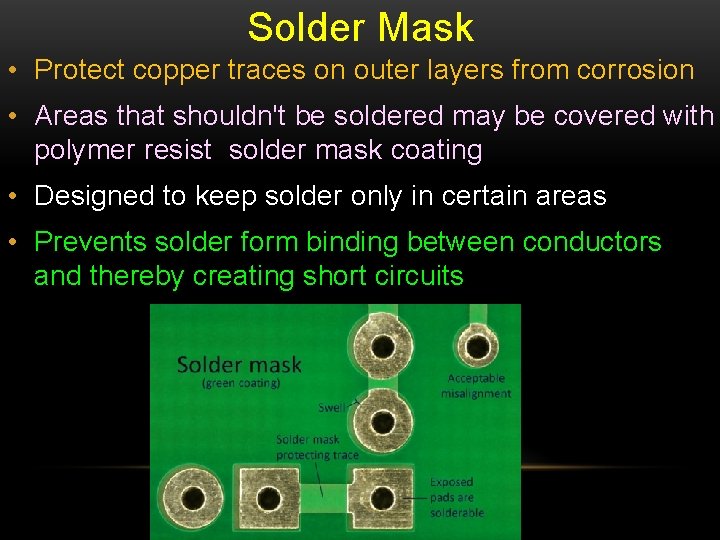
Solder Mask • Protect copper traces on outer layers from corrosion • Areas that shouldn't be soldered may be covered with polymer resist solder mask coating • Designed to keep solder only in certain areas • Prevents solder form binding between conductors and thereby creating short circuits

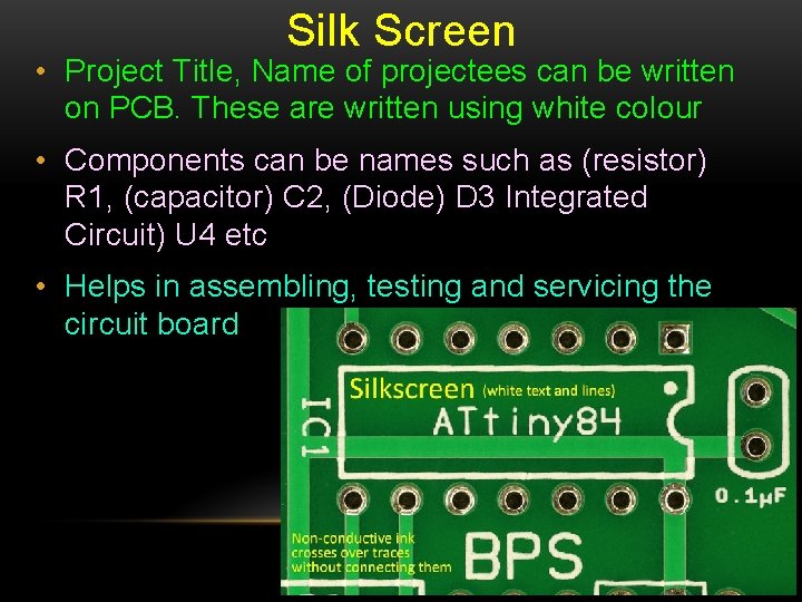
Silk Screen • Project Title, Name of projectees can be written on PCB. These are written using white colour • Components can be names such as (resistor) R 1, (capacitor) C 2, (Diode) D 3 Integrated Circuit) U 4 etc • Helps in assembling, testing and servicing the circuit board