Shri Sant Gajanan Maharaj College of Engineering Department

- Slides: 71

Shri Sant Gajanan Maharaj College of Engineering Department of Electronics & Telecommunications Engineering Electronic Devices & Components Unit – V Special Purpose Diodes Varactor Diode and Schottky Diode

Topics under Unit-V Theory, Construction, Characteristics and Applications of Tunnel, Varactor, Schottky Diode Opto-Devices: LED, Photodiode, LCD

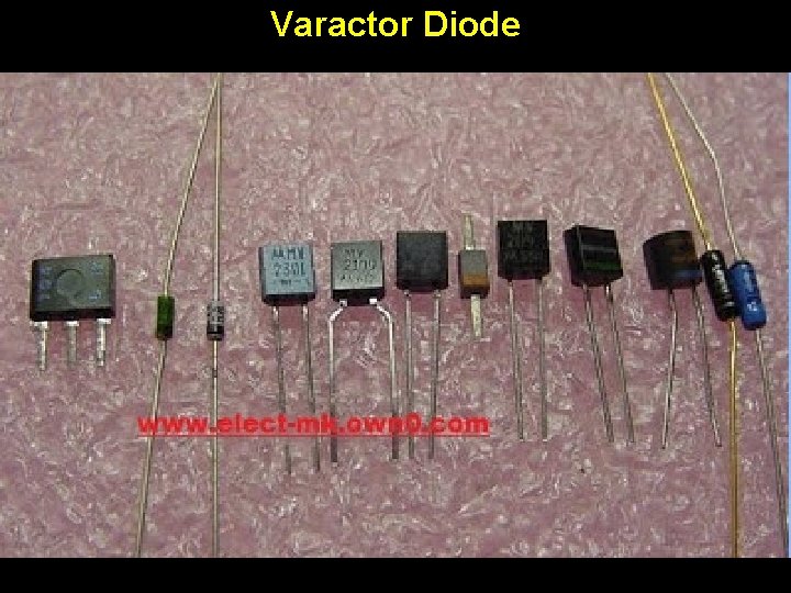
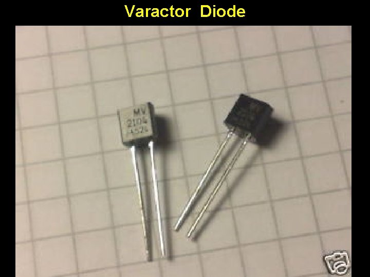
Varactor Diode

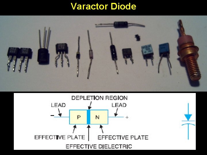
Varactor Diode

Varactor Diode

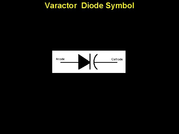
Varactor Diode Symbol

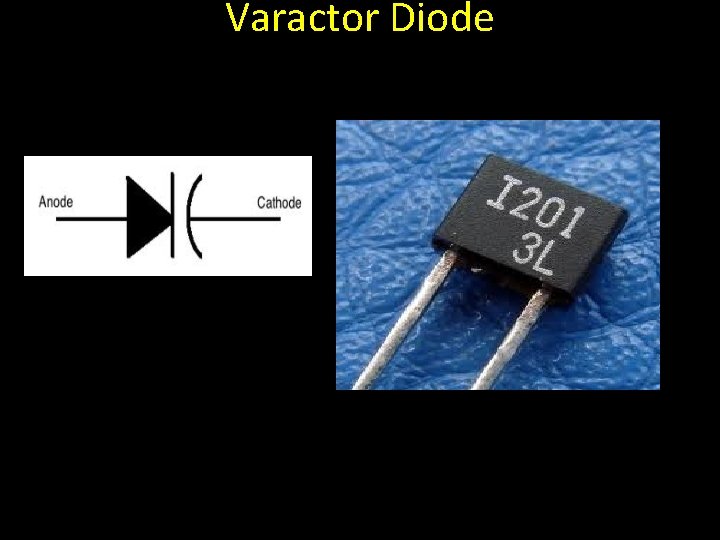
Varactor Diode

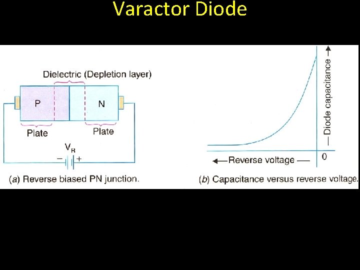
Varactor Diode

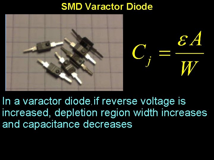
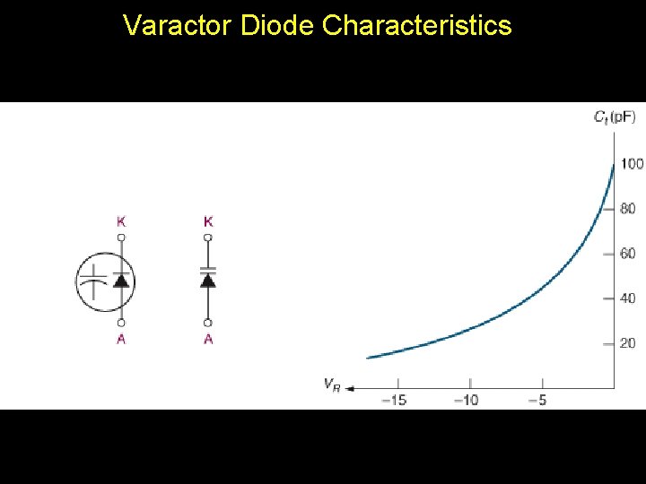
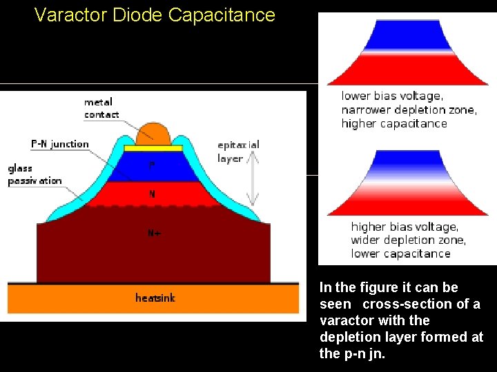
SMD Varactor Diode In a varactor diode, if reverse voltage is increased, depletion region width increases and capacitance decreases

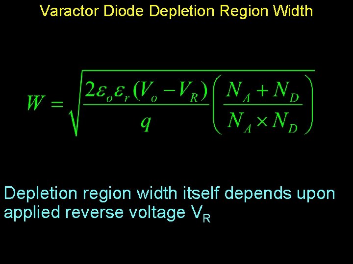
Varactor Diode Depletion Region Width Depletion region width itself depends upon applied reverse voltage VR

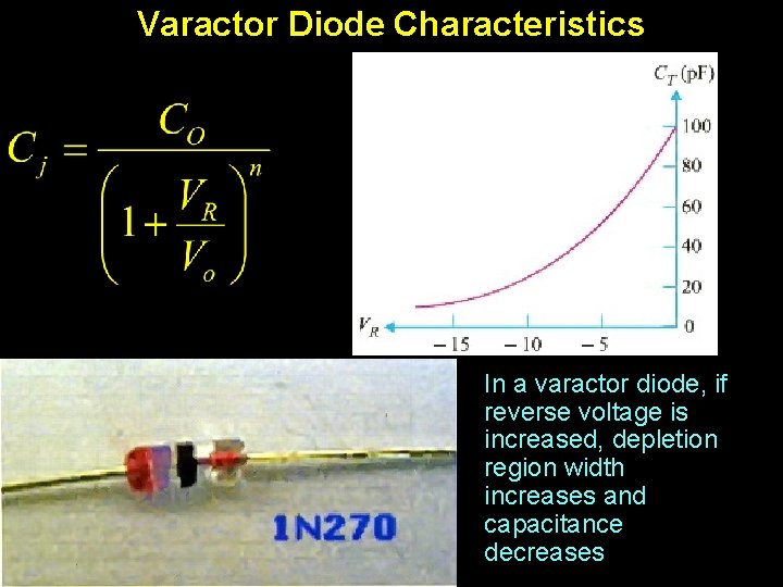
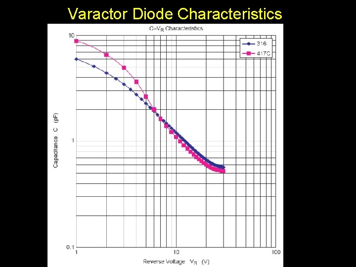
Varactor Diode Characteristics In a varactor diode, if reverse voltage is increased, depletion region width increases and capacitance decreases

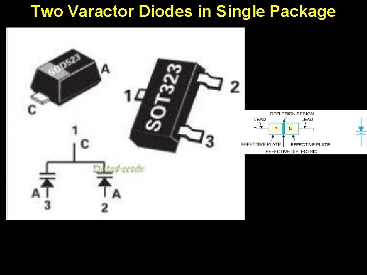
Two Varactor Diodes in Single Package

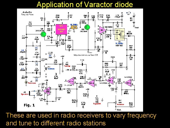
Application of Varactor diode These are used in radio receivers to vary frequency and tune to different radio stations

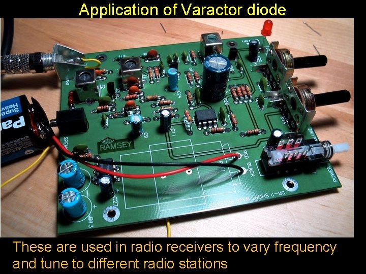
Application of Varactor diode These are used in radio receivers to vary frequency and tune to different radio stations

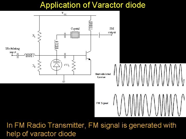
Application of Varactor diode In FM Radio Transmitter, FM signal is generated with help of varactor diode

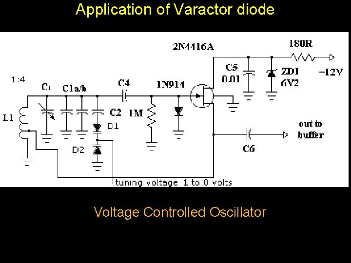
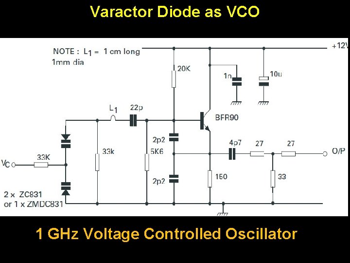
Application of Varactor diode Voltage Controlled Oscillator

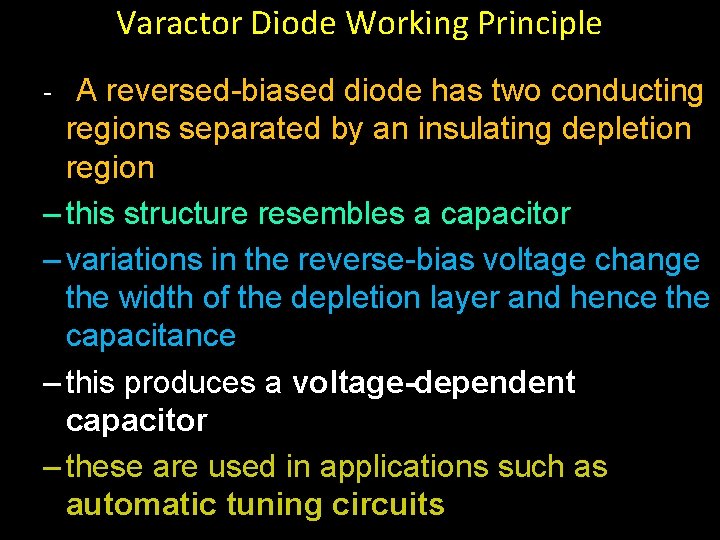
Varactor Diode Working Principle - A reversed-biased diode has two conducting regions separated by an insulating depletion region – this structure resembles a capacitor – variations in the reverse-bias voltage change the width of the depletion layer and hence the capacitance – this produces a voltage-dependent capacitor – these are used in applications such as automatic tuning circuits

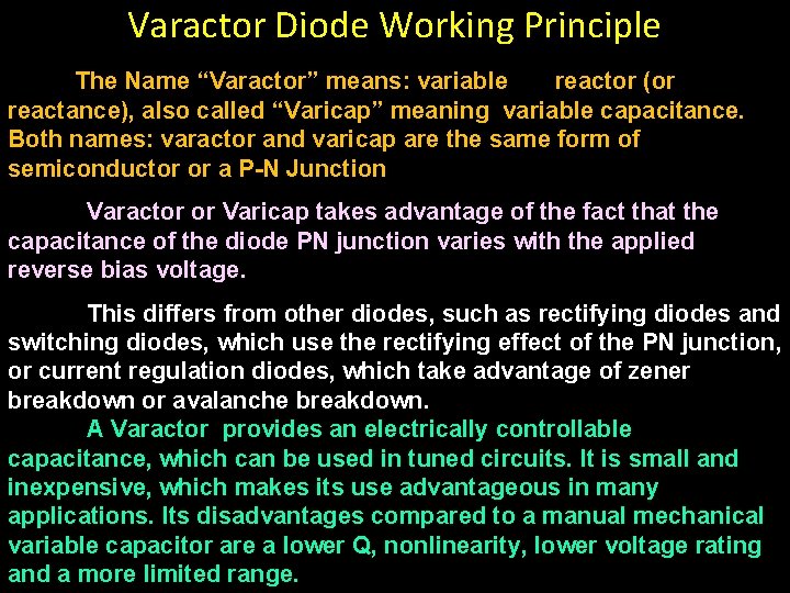
Varactor Diode Working Principle The Name “Varactor” means: variable reactor (or reactance), also called “Varicap” meaning variable capacitance. Both names: varactor and varicap are the same form of semiconductor or a P-N Junction Varactor or Varicap takes advantage of the fact that the capacitance of the diode PN junction varies with the applied reverse bias voltage. This differs from other diodes, such as rectifying diodes and switching diodes, which use the rectifying effect of the PN junction, or current regulation diodes, which take advantage of zener breakdown or avalanche breakdown. A Varactor provides an electrically controllable capacitance, which can be used in tuned circuits. It is small and inexpensive, which makes its use advantageous in many applications. Its disadvantages compared to a manual mechanical variable capacitor are a lower Q, nonlinearity, lower voltage rating and a more limited range.

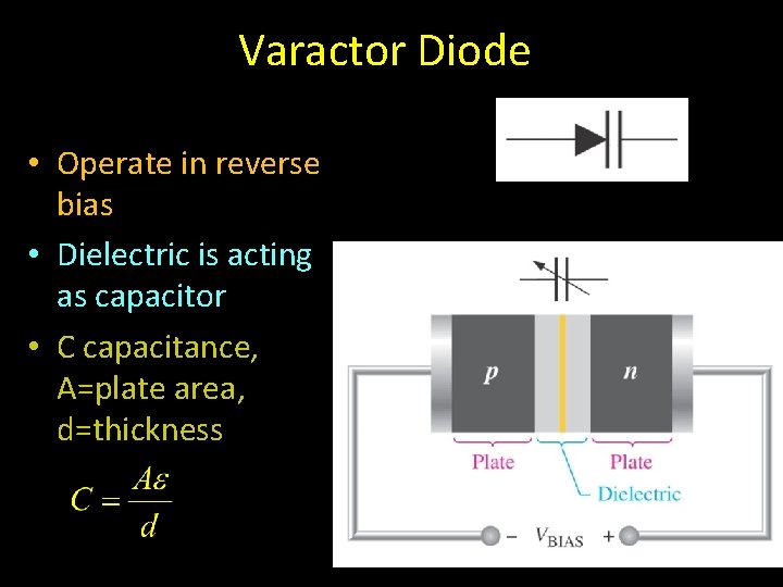
Varactor Diode • Operate in reverse bias • Dielectric is acting as capacitor • C capacitance, A=plate area, d=thickness

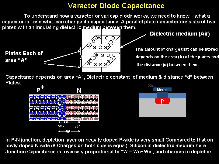
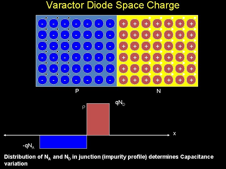
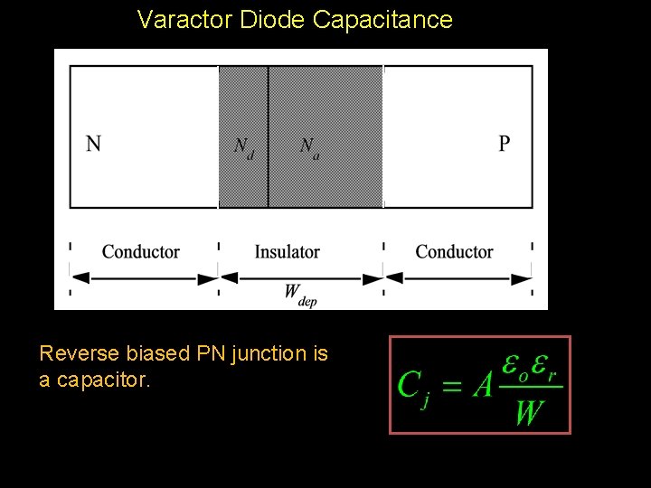
Varactor Diode Capacitance To understand how a varactor or varicap diode works, we need to know “what a capacitor is” and what can change its capacitance. A parallel plate capacitor consists of two plates with an insulating dielectric medium between them. Dielectric medium (Air) The amount of charge that can be stored Plates Each of area “A” d depends on the area (A) of the plates and the distance (d) between them. Capacitance depends on area “A”, Dielectric constant of medium & distance “d” between Plates. P+ N - - - - - +++++ - - - - -- -- + + + + + - - - - --- + + + + + - - - - -- -- + + + + + - - - - - +++++ Sio 2 Metal p Wp Wn W In P-N junction, depletion layer on heavily doped P-side is very small Compared to that on lowly doped N-side (# Charges on both side is equal). Silicon is dielectric medium here. Junction Capacitance is inversely proportional to “W = Wn+Wp , and charges in depletion.

Varactor Diode Space Charge - - - - - - - + + + + + + + - - - - + + + + P N q. ND x -q. NA Distribution of NA and ND in junction (impurity profile) determines Capacitance variation

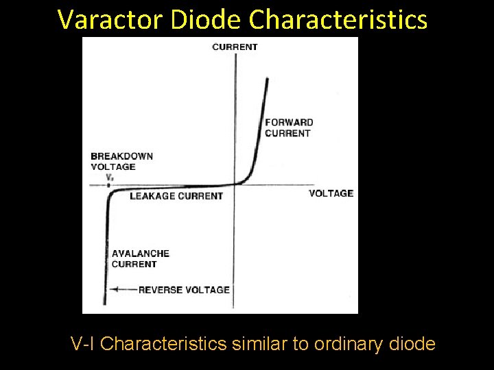
Varactor Diode Characteristics V-I Characteristics similar to ordinary diode

Varactor Diode Capacitance Reverse biased PN junction is a capacitor.

Varactor Diode Characteristics

Varactor Diode Capacitance Internal structure of a varicap In the figure it can be seen cross-section of a varactor with the depletion layer formed at the p-n jn.

Varactor Diode Characteristics

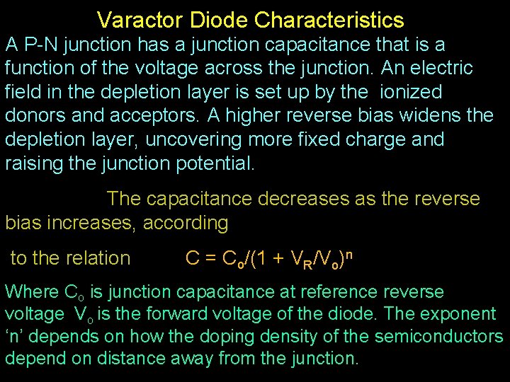
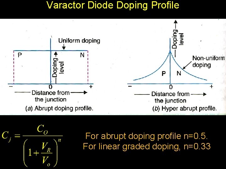
Varactor Diode Characteristics A P-N junction has a junction capacitance that is a function of the voltage across the junction. An electric field in the depletion layer is set up by the ionized donors and acceptors. A higher reverse bias widens the depletion layer, uncovering more fixed charge and raising the junction potential. The capacitance decreases as the reverse bias increases, according to the relation C = Co/(1 + VR/Vo)n Where Co is junction capacitance at reference reverse voltage Vo is the forward voltage of the diode. The exponent ‘n’ depends on how the doping density of the semiconductors depend on distance away from the junction.

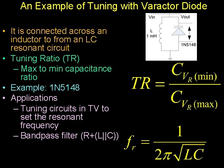
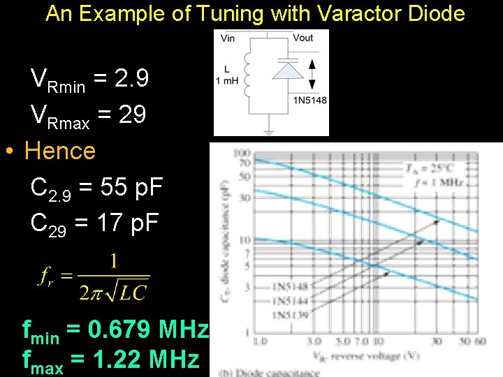
An Example of Tuning with Varactor Diode • It is connected across an inductor to from an LC resonant circuit • Tuning Ratio (TR) – Max to min capacitance ratio • Example: 1 N 5148 • Applications – Tuning circuits in TV to set the resonant frequency – Bandpass filter (R+(L||C))

An Example of Tuning with Varactor Diode VRmin = 2. 9 VRmax = 29 • Hence C 2. 9 = 55 p. F C 29 = 17 p. F fmin = 0. 679 MHz fmax = 1. 22 MHz

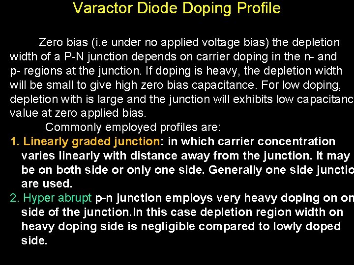
Varactor Diode Doping Profile Zero bias (i. e under no applied voltage bias) the depletion width of a P-N junction depends on carrier doping in the n- and p- regions at the junction. If doping is heavy, the depletion width will be small to give high zero bias capacitance. For low doping, depletion with is large and the junction will exhibits low capacitance value at zero applied bias. Commonly employed profiles are: 1. Linearly graded junction: in which carrier concentration varies linearly with distance away from the junction. It may be on both side or only one side. Generally one side junctio are used. 2. Hyper abrupt p-n junction employs very heavy doping on on side of the junction. In this case depletion region width on heavy doping side is negligible compared to lowly doped side.

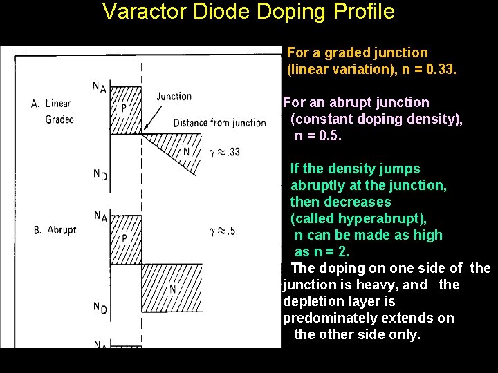
Varactor Diode Doping Profile For abrupt doping profile n=0. 5. For linear graded doping, n=0. 33

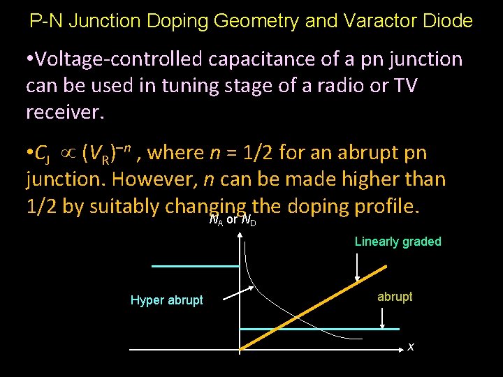
P-N Junction Doping Geometry and Varactor Diode • Voltage-controlled capacitance of a pn junction can be used in tuning stage of a radio or TV receiver. • CJ (VR)–n , where n = 1/2 for an abrupt pn junction. However, n can be made higher than 1/2 by suitably changing the doping profile. N or N A D Linearly graded Hyper abrupt x

Varactor Diode Doping Profile For a graded junction (linear variation), n = 0. 33. For an abrupt junction (constant doping density), n = 0. 5. If the density jumps abruptly at the junction, then decreases (called hyperabrupt), n can be made as high as n = 2. The doping on one side of the junction is heavy, and the depletion layer is predominately extends on the other side only.

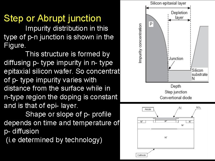
Step or Abrupt junction Impurity distribution in this type of p-n junction is shown in the Figure. This structure is formed by diffusing p- type impurity in n- type epitaxial silicon wafer. So concentration of p- type impurity varies with distance from the surface while in n-type region the doping is constant and is that of epi- layer. Shape or slope of p- profile depends on time and temperature of p- diffusion (i. e determined by technology)

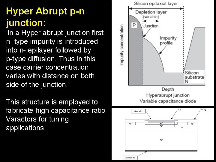
Hyper Abrupt p-n junction: In a Hyper abrupt junction first n- type impurity is introduced into n- epilayer followed by p-type diffusion. Thus in this case carrier concentration varies with distance on both side of the junction. This structure is employed to fabricate high capacitance ratio Varactors for tuning applications

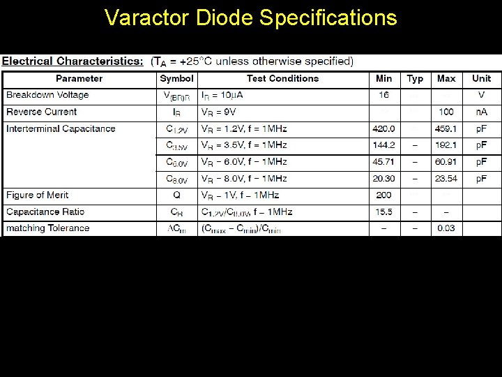
Varactor Diode Specifications

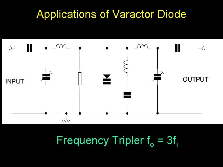
Applications of Varactor Diode • Frequency Multipliers - used in applications where it’s difficult to generate microwave signals. • Producing relatively high power outputs at frequencies up to 100 GHz.

Applications of Varactor Diode Frequency Tripler fo = 3 fi

Applications of Varactor Diode • Parametric Amplifiers. - named for the timevarying parameter, or value of capacitance, associated with the operation. • Since the underlying principle of operation is based on reactance, the parametric amplifier is sometimes called a REACTANCE AMPLIFIER.

Applications of Varactor Diode • Tuning - Since the frequency can be made to vary they are used as electronic tuning devices in tuners for television, mobiles. • Other Applications: They are used in PLL, voltage controlled oscillators, harmonic generation, electronic tuning devices in tuners for television, mobiles, parametric amplification, AM radios, voltage-variable tuning, frequency multipliers, etc.

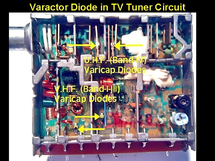
Varactor Diode in TV Tuner Circuit

Varactor Diode as VCO 1 GHz Voltage Controlled Oscillator

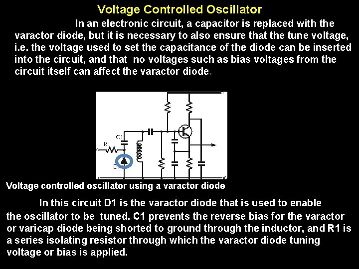
Voltage Controlled Oscillator In an electronic circuit, a capacitor is replaced with the varactor diode, but it is necessary to also ensure that the tune voltage, i. e. the voltage used to set the capacitance of the diode can be inserted into the circuit, and that no voltages such as bias voltages from the circuit itself can affect the varactor diode. Voltage controlled oscillator using a varactor diode In this circuit D 1 is the varactor diode that is used to enable the oscillator to be tuned. C 1 prevents the reverse bias for the varactor or varicap diode being shorted to ground through the inductor, and R 1 is a series isolating resistor through which the varactor diode tuning voltage or bias is applied.

Schottky Diode

Schottky Diode

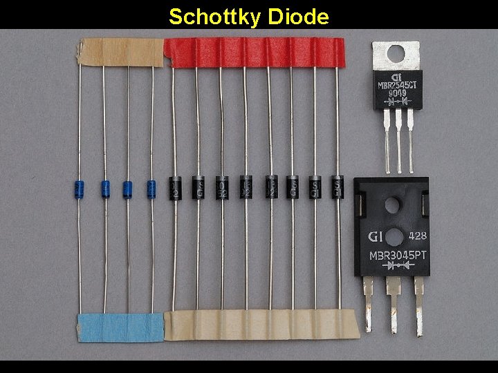
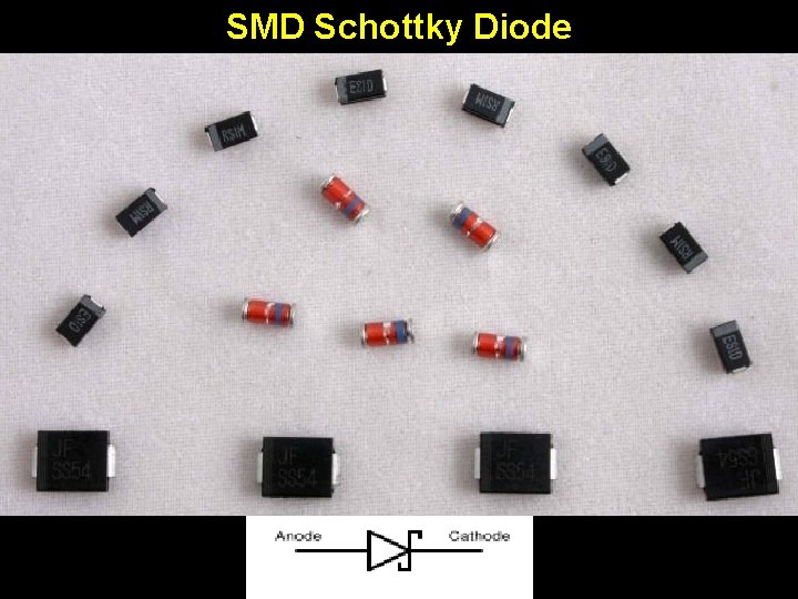
SMD Schottky Diode

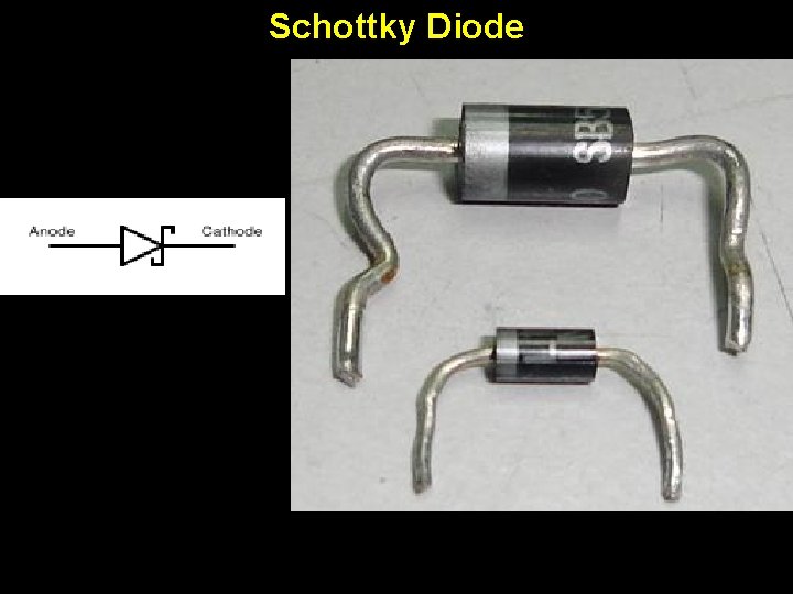
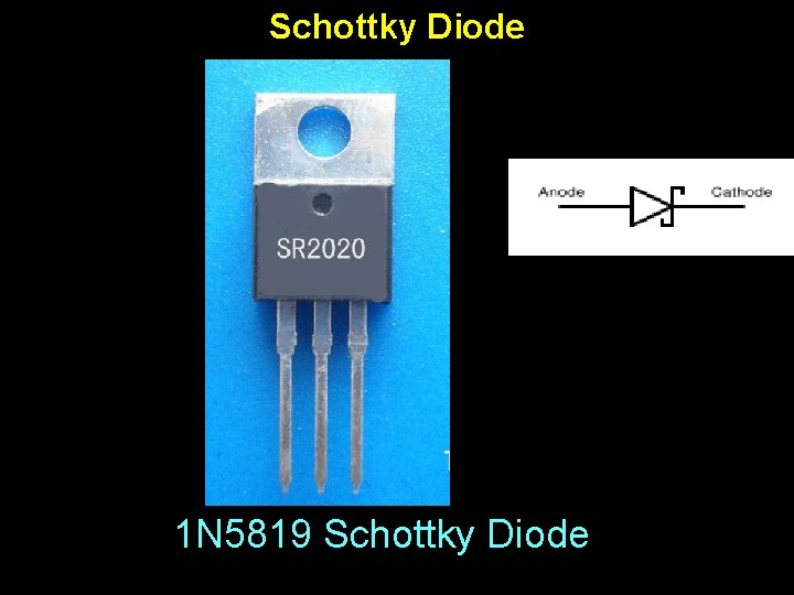
Schottky Diode 1 N 5819 Schottky Diode

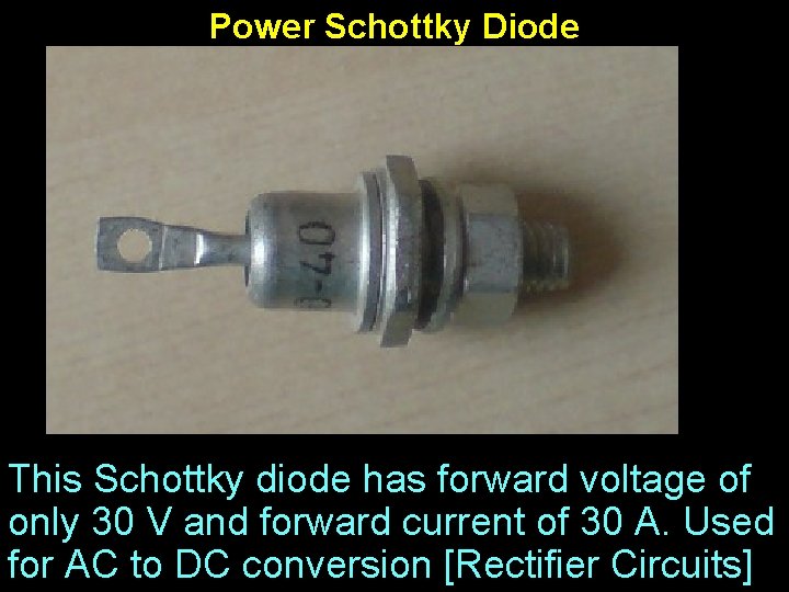
Power Schottky Diode This Schottky diode has forward voltage of only 30 V and forward current of 30 A. Used for AC to DC conversion [Rectifier Circuits]

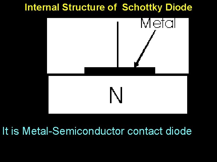
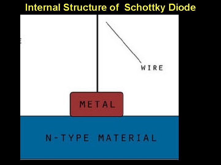
Internal Structure of Schottky Diode It is Metal-Semiconductor contact diode

Internal Structure of Schottky Diode

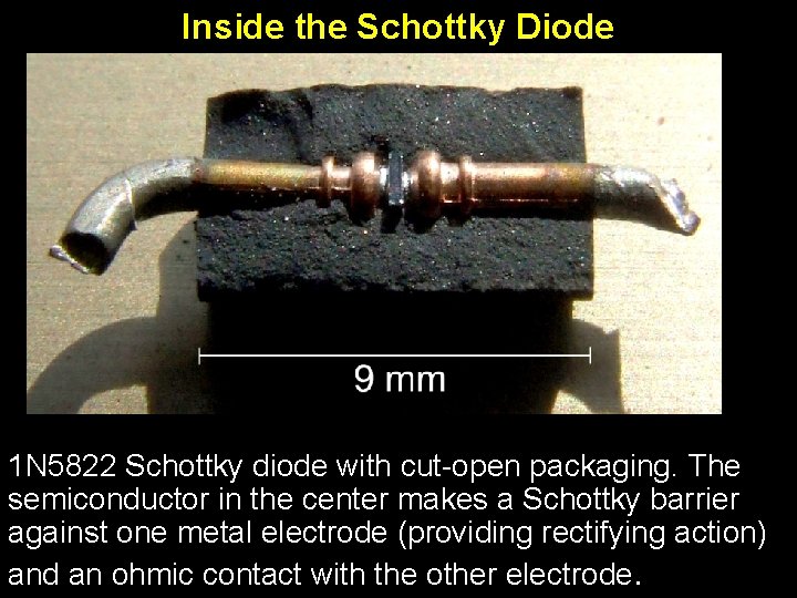
Inside the Schottky Diode 1 N 5822 Schottky diode with cut-open packaging. The semiconductor in the center makes a Schottky barrier against one metal electrode (providing rectifying action) and an ohmic contact with the other electrode.

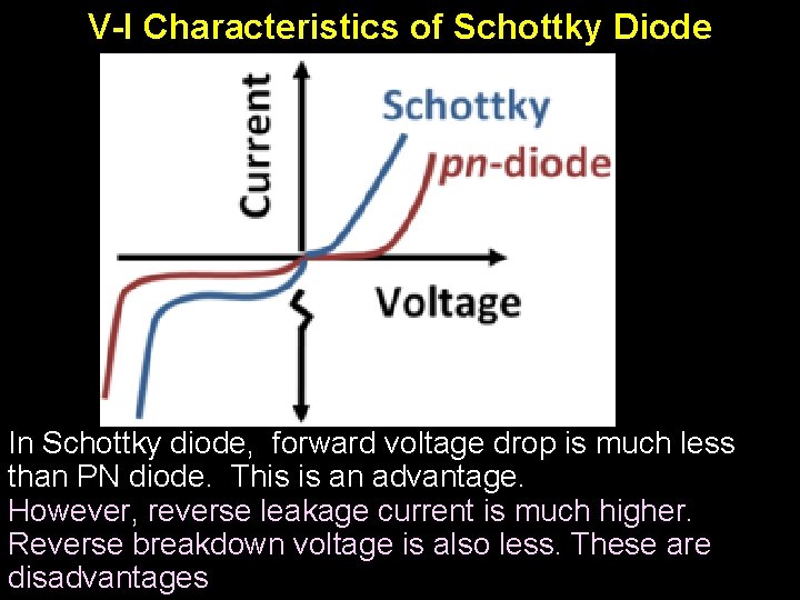
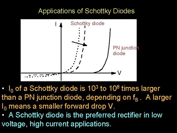
V-I Characteristics of Schottky Diode In Schottky diode, forward voltage drop is much less than PN diode. This is an advantage. However, reverse leakage current is much higher. Reverse breakdown voltage is also less. These are disadvantages

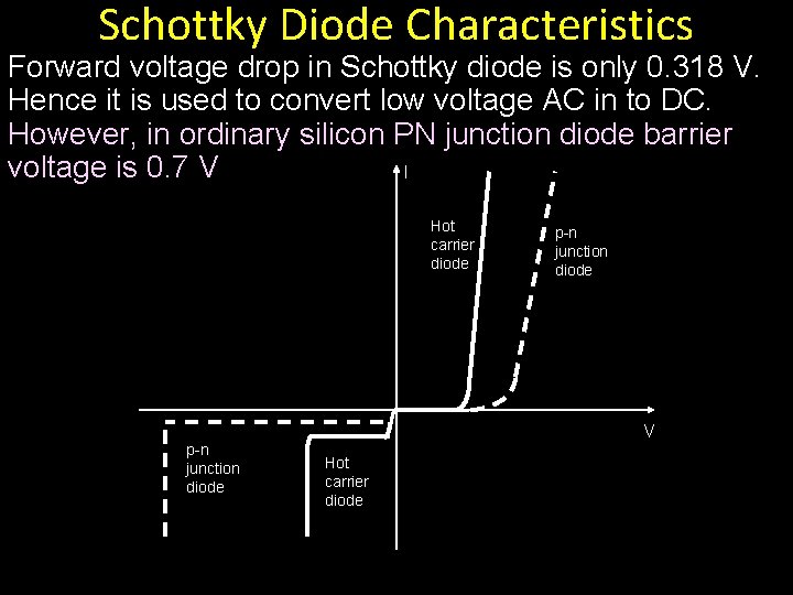
Schottky Diode Characteristics Forward voltage drop in Schottky diode is only 0. 318 V. Hence it is used to convert low voltage AC in to DC. However, in ordinary silicon PN junction diode barrier voltage is 0. 7 V I Hot carrier diode p-n junction diode V p-n junction diode Hot carrier diode

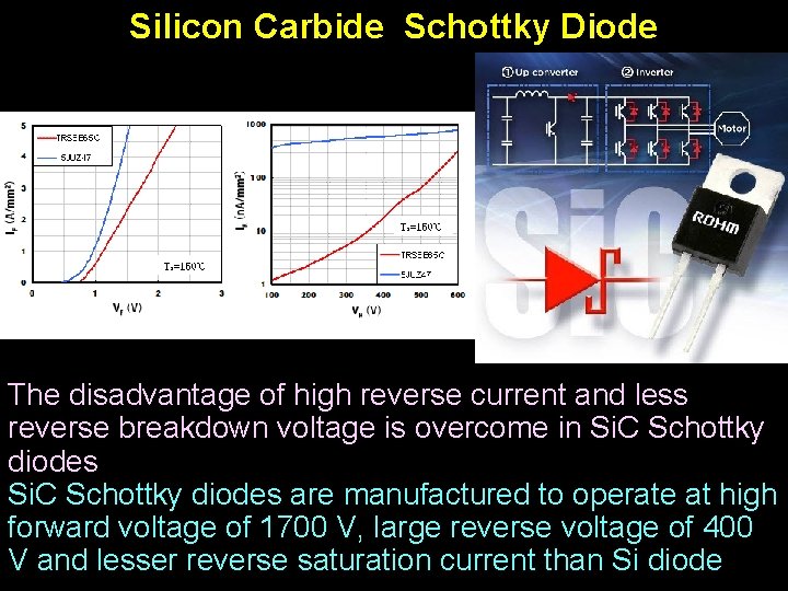
Silicon Carbide Schottky Diode The disadvantage of high reverse current and less reverse breakdown voltage is overcome in Si. C Schottky diodes are manufactured to operate at high forward voltage of 1700 V, large reverse voltage of 400 V and lesser reverse saturation current than Si diode

Schottky Diode • Also known as Hot Carrier Diode, is a semiconductor diode with a low forward voltage drop and a very fast switching action. • When current flows through a diode there is a small voltage drop across the diode terminals. A normal silicon diode has a voltage drop between 0. 6– 1. 7 volts, while a Schottky diode voltage drop is between approximately 0. 15– 0. 45 volts. This lower voltage drop can provide higher switching speed and better system efficiency.

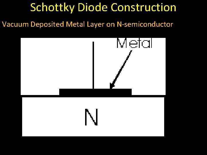
Schottky Diode Construction • A metal–semiconductor junction is formed between a metal and a semiconductor, creating a Schottky barrier (instead of a semiconductor– semiconductor junction as in conventional diodes). • Typical metals used are molybdenum, platinum, chromium or tungsten; and the semiconductor would typically be N-type silicon. • The metal side acts as the anode and N-type semiconductor acts as the cathode of the diode. This Schottky barrier results in both very fast switching and low forward voltage drop.

Reverse Recovery Time of Schottky Diode • The most important difference between the p-n and Schottky diode is reverse recovery time, when the diode switches from conducting to nonconducting state. Where in a p-n diode the reverse recovery time can be in the order of hundreds of nanoseconds and less than 100 ns for fast diodes, Schottky diodes do not have a recovery time, as there is nothing to recover from (i. e. no charge carrier depletion region at the junction). • The switching time is ~100 ps for the small signal diodes, and up to tens of nanoseconds for special high-capacity power diodes.

Why Switching Speed is Higher • It is often said that the Schottky diode is a majority carrier semiconductor device. This means that if the semiconductor body is doped n-type, only the n-type carriers (mobile electron) play a significant role in normal operation of the device. The majority carriers are quickly injected into the conduction band of the metal contact on the other side of the diode to become free moving electron. Therefore no slow, random recombination of n- and p- type carriers is involved, so that this diode can stop conduction faster than an ordinary p-n rectifier diode. This property in turn allows a smaller device area, which also makes for a faster transition.

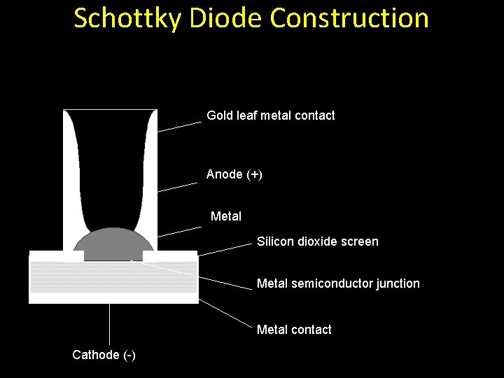
Schottky Diode Construction Gold leaf metal contact Anode (+) Metal Silicon dioxide screen Metal semiconductor junction Metal contact Cathode (-)

Schottky Diode Construction Vacuum Deposited Metal Layer on N-semiconductor

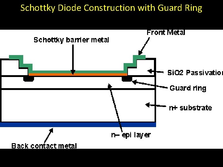
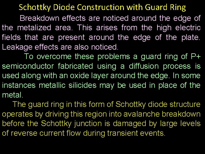
Schottky Diode Construction with Guard Ring

Schottky Diode Construction with Guard Ring Breakdown effects are noticed around the edge of the metalized area. This arises from the high electric fields that are present around the edge of the plate. Leakage effects are also noticed. To overcome these problems a guard ring of P+ semiconductor fabricated using a diffusion process is used along with an oxide layer around the edge. In some instances metallic silicides may be used in place of the metal. The guard ring in this form of Schottky diode structure operates by driving this region into avalanche breakdown before the Schottky junction is damaged by large levels of reverse current flow during transient events.

Disadvantages of Schottky Diode • The most evident limitations of Schottky diodes are the relatively low reverse voltage ratings for silicon-metal Schottky diodes, typically 50 V and below, and a relatively high reverse leakage current. Some higher-voltage designs are available; 200 V is considered a high reverse voltage. • Reverse leakage current, because it increases with temperature, leads to a thermal instability issue. This often limits the useful reverse voltage to well below the actual rating.

Advantages of Schottky Diode • Low turn on voltage: The turn-on voltage for the diode is between 0. 2 and 0. 3 volts for a Schottky diode against 0. 6 to 0. 7 volts for a standard silicon diode. • Fast recovery time: The fast recovery time because of the small amount of stored charge means that it can be used for high speed switching applications. • Low junction capacitance: In view of the very small active area, often as a result of using a wire point contact onto the silicon, the capacitance levels are very small.

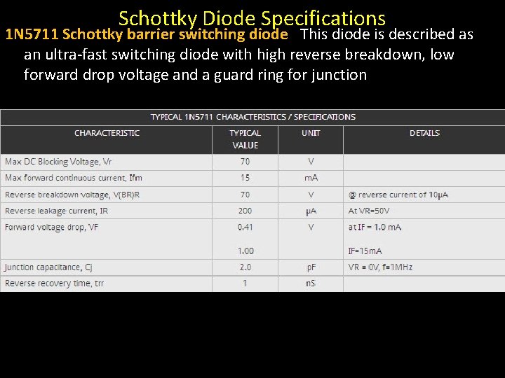
Schottky Diode Specifications 1 N 5711 Schottky barrier switching diode This diode is described as an ultra-fast switching diode with high reverse breakdown, low forward drop voltage and a guard ring for junction

Applications of Schottky Diodes I I Schottky diode f B PN junction diode V V • I 0 of a Schottky diode is 103 to 108 times larger than a PN junction diode, depending on f. B. A larger I 0 means a smaller forward drop V. • A Schottky diode is the preferred rectifier in low voltage, high current applications.

Areas of Applications of Schottky Diode Lower noise figure Low-voltage or high-current power supplies AC-to-DC converters Radar Systems Schottky TTL logic (High speed digital ICs)

Applications of Schottky Diode RF mixer and detector diode: The Schottky diode has come into its own for radio frequency applications because of its high switching speed and high frequency capability. In view of this Schottky barrier diodes are used in many high performance diode ring mixers. In addition to this their low turn on voltage and high frequency capability and low capacitance make them ideal as RF detectors. Power rectifier: Schottky barrier diodes are also used in high power applications, as rectifiers. Their high current density and low forward voltage drop mean that less power is wasted than if ordinary PN junction diodes were used. This increase in efficiency means that less heat has to be dissipated, and smaller heat sinks may be able to be incorporated in the design.

Applications of Schottky Diode Power OR circuits: Schottky diodes can be used in applications where a load is driven by two separate power supplies. One example may be a mains power supply and a battery supply. In these instances it is necessary that the power from one supply does not enter the other. This can be achieved using diodes. However it is important that any voltage drop across the diodes is minimized to ensure maximum efficiency. As in many other applications, this diode is ideal for this in view of its low forward voltage drop.

Applications of Schottky Diode Solar cell applications: Solar cells are typically connected to rechargeable batteries, often lead acid batteries because power may be required 24 hours a day and the Sun is not always available. Solar cells do not like the reverse charge applied and therefore a diode is required in series with the solar cells. Any voltage drop will result in a reduction in efficiency and therefore a low voltage drop diode is needed. As in other applications, the low voltage drop of the Schottky diode is particularly useful, and as a result they are the favoured form of diode in this application.

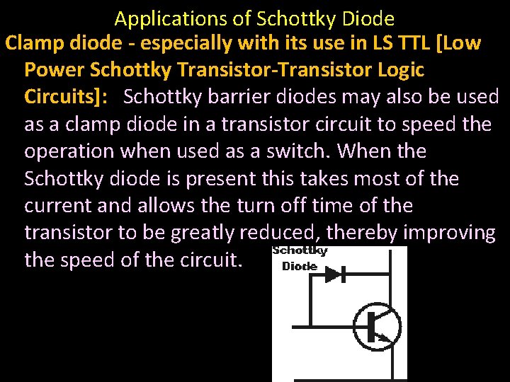
Applications of Schottky Diode Clamp diode - especially with its use in LS TTL [Low Power Schottky Transistor-Transistor Logic Circuits]: Schottky barrier diodes may also be used as a clamp diode in a transistor circuit to speed the operation when used as a switch. When the Schottky diode is present this takes most of the current and allows the turn off time of the transistor to be greatly reduced, thereby improving the speed of the circuit.