Shri Sant Gajanan Maharaj College of Engineering Department
![Application of PCB [Copper Clad Laminates] From schematic, PCB Layout is drawn and the Application of PCB [Copper Clad Laminates] From schematic, PCB Layout is drawn and the](https://slidetodoc.com/presentation_image/20bffd2e55099b24e907673326c21a24/image-7.jpg)
![Application of PCB [Copper Clad Laminates] From schematic, PCB Layout is drawn and the Application of PCB [Copper Clad Laminates] From schematic, PCB Layout is drawn and the](https://slidetodoc.com/presentation_image/20bffd2e55099b24e907673326c21a24/image-8.jpg)
![Application of PCB [Copper Clad Laminates] Drawing PCB Layout is an art. Some rules Application of PCB [Copper Clad Laminates] Drawing PCB Layout is an art. Some rules](https://slidetodoc.com/presentation_image/20bffd2e55099b24e907673326c21a24/image-9.jpg)
![Application of PCB [Copper Clad Laminates] The layout may drawn by hand on trace Application of PCB [Copper Clad Laminates] The layout may drawn by hand on trace](https://slidetodoc.com/presentation_image/20bffd2e55099b24e907673326c21a24/image-10.jpg)
![Application of PCB [Copper Clad Laminates] The layout may drawn by hand on trace Application of PCB [Copper Clad Laminates] The layout may drawn by hand on trace](https://slidetodoc.com/presentation_image/20bffd2e55099b24e907673326c21a24/image-11.jpg)
![Application of PCB [Copper Clad Laminates] The solder side and Component side are shown. Application of PCB [Copper Clad Laminates] The solder side and Component side are shown.](https://slidetodoc.com/presentation_image/20bffd2e55099b24e907673326c21a24/image-12.jpg)
![Classification of PCBs According to Base Material PTFE Polyamide [Nylon] Epoxy Resin Phenolic Classification of PCBs According to Base Material PTFE Polyamide [Nylon] Epoxy Resin Phenolic](https://slidetodoc.com/presentation_image/20bffd2e55099b24e907673326c21a24/image-27.jpg)
![Electrical Property of Copper Clad Laminate (01) Volume Resistivity [continued]: The volume resistance is Electrical Property of Copper Clad Laminate (01) Volume Resistivity [continued]: The volume resistance is](https://slidetodoc.com/presentation_image/20bffd2e55099b24e907673326c21a24/image-31.jpg)
![Electrical Property of Copper Clad Laminate (04) Dielectric Constant [continued]: Lesser the value of Electrical Property of Copper Clad Laminate (04) Dielectric Constant [continued]: Lesser the value of](https://slidetodoc.com/presentation_image/20bffd2e55099b24e907673326c21a24/image-37.jpg)
![Electrical Property of Copper Clad Laminate (04) Dielectric Loss [continued]: The dielectric loss is Electrical Property of Copper Clad Laminate (04) Dielectric Loss [continued]: The dielectric loss is](https://slidetodoc.com/presentation_image/20bffd2e55099b24e907673326c21a24/image-39.jpg)

![Characteristics of Base Materials of PCB (02) Polyamide Resin [Nylon] They have good mechanical Characteristics of Base Materials of PCB (02) Polyamide Resin [Nylon] They have good mechanical](https://slidetodoc.com/presentation_image/20bffd2e55099b24e907673326c21a24/image-55.jpg)
- Slides: 67

Shri Sant Gajanan Maharaj College of Engineering Department of Electronics & Telecommunications Engineering Electronic Devices & Components Unit – III Printed Circuit Board Manufacturing Process , Development Process and Soldering Techniques PCB Types, Materials, Characteristics and Manufacturing Process

References (a) Introduction to Printed Circuit Boards by Anand & Anand (b) Printed Circuit Boards by Khandpur (c) Electronic materials and Components by S. M. Dhir (d) Many Internet Resources

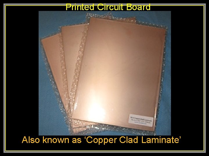
Printed Circuit Board Also known as ‘Copper Clad Laminate’

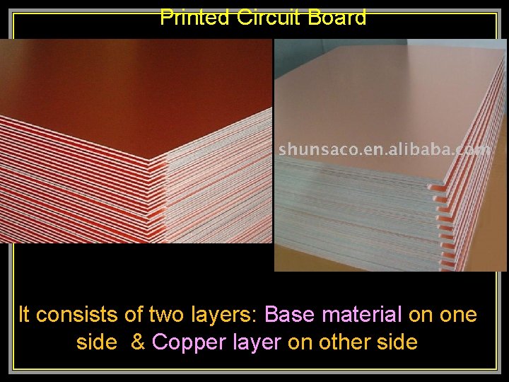
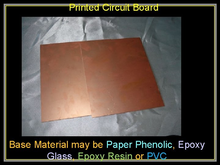
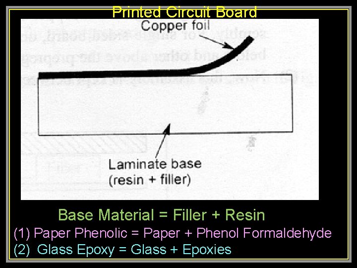
Printed Circuit Board It consists of two layers: Base material on one side & Copper layer on other side

Printed Circuit Board Base Material may be Paper Phenolic, Epoxy Glass, Epoxy Resin or PVC

Printed Circuit Board Base Material = Filler + Resin (1) Paper Phenolic = Paper + Phenol Formaldehyde (2) Glass Epoxy = Glass + Epoxies
![Application of PCB Copper Clad Laminates From schematic PCB Layout is drawn and the Application of PCB [Copper Clad Laminates] From schematic, PCB Layout is drawn and the](https://slidetodoc.com/presentation_image/20bffd2e55099b24e907673326c21a24/image-7.jpg)
Application of PCB [Copper Clad Laminates] From schematic, PCB Layout is drawn and the pattern is then transferred on the PCB
![Application of PCB Copper Clad Laminates From schematic PCB Layout is drawn and the Application of PCB [Copper Clad Laminates] From schematic, PCB Layout is drawn and the](https://slidetodoc.com/presentation_image/20bffd2e55099b24e907673326c21a24/image-8.jpg)
Application of PCB [Copper Clad Laminates] From schematic, PCB Layout is drawn and the pattern is then transferred on the PCB
![Application of PCB Copper Clad Laminates Drawing PCB Layout is an art Some rules Application of PCB [Copper Clad Laminates] Drawing PCB Layout is an art. Some rules](https://slidetodoc.com/presentation_image/20bffd2e55099b24e907673326c21a24/image-9.jpg)
Application of PCB [Copper Clad Laminates] Drawing PCB Layout is an art. Some rules are laid down for efficient layout drawing
![Application of PCB Copper Clad Laminates The layout may drawn by hand on trace Application of PCB [Copper Clad Laminates] The layout may drawn by hand on trace](https://slidetodoc.com/presentation_image/20bffd2e55099b24e907673326c21a24/image-10.jpg)
Application of PCB [Copper Clad Laminates] The layout may drawn by hand on trace paper or through software like Express. PCB, Dip. Trace, Eagle, Ultiboard
![Application of PCB Copper Clad Laminates The layout may drawn by hand on trace Application of PCB [Copper Clad Laminates] The layout may drawn by hand on trace](https://slidetodoc.com/presentation_image/20bffd2e55099b24e907673326c21a24/image-11.jpg)
Application of PCB [Copper Clad Laminates] The layout may drawn by hand on trace paper or through software like Express. PCB, Dip. Trace, Eagle, Ultiboard
![Application of PCB Copper Clad Laminates The solder side and Component side are shown Application of PCB [Copper Clad Laminates] The solder side and Component side are shown.](https://slidetodoc.com/presentation_image/20bffd2e55099b24e907673326c21a24/image-12.jpg)
Application of PCB [Copper Clad Laminates] The solder side and Component side are shown. IC sockets must be soldered and then ICs must be inserted in to them.

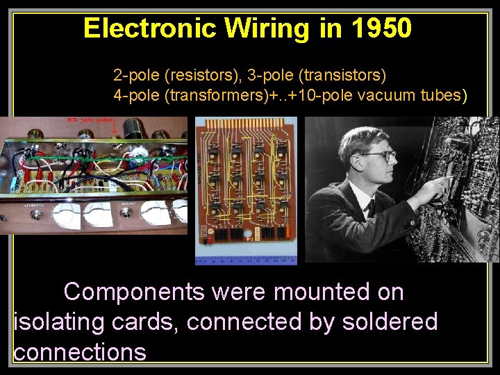
Electronic Wiring in 1950 2 -pole (resistors), 3 -pole (transistors) 4 -pole (transformers)+. . +10 -pole vacuum tubes) Components were mounted on isolating cards, connected by soldered connections

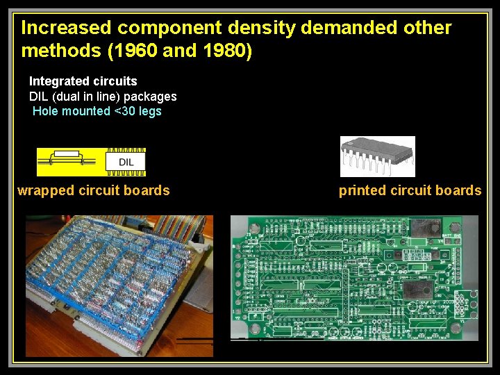
Increased component density demanded other methods (1960 and 1980) Integrated circuits DIL (dual in line) packages Hole mounted <30 legs wrapped circuit boards printed circuit boards

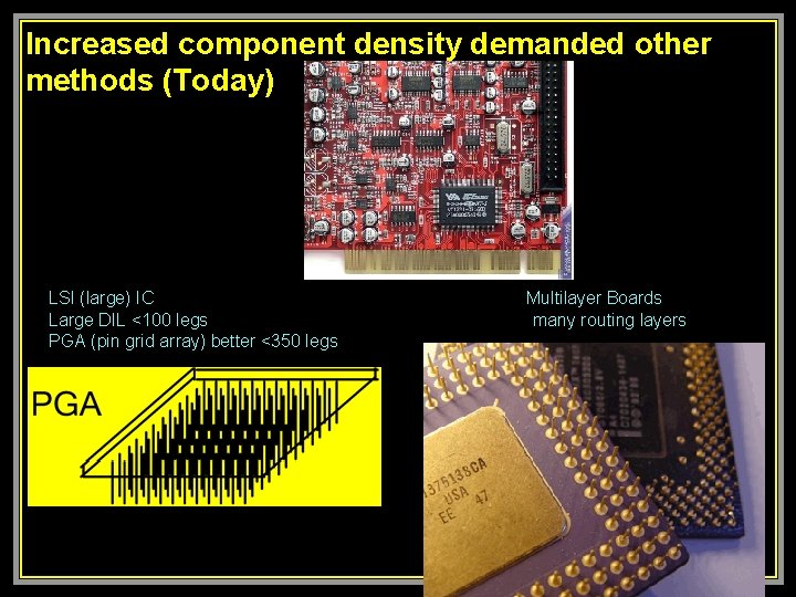
Increased component density demanded other methods (Today) LSI (large) IC Large DIL <100 legs PGA (pin grid array) better <350 legs Multilayer Boards many routing layers

Classification of PCBs According to Sides Single Side PCB Double Sided PCB Multilayer PCB

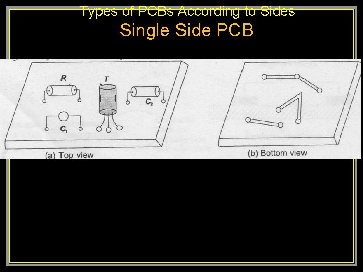
Types of PCBs According to Sides Single Side PCB

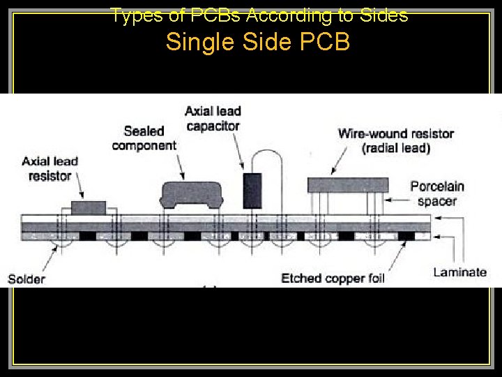
Types of PCBs According to Sides Single Side PCB

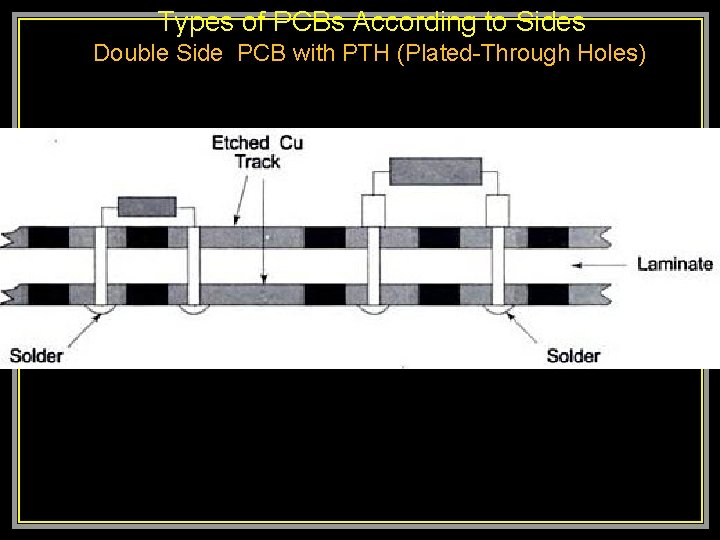
Types of PCBs According to Sides Double Side PCB with PTH (Plated-Through Holes)

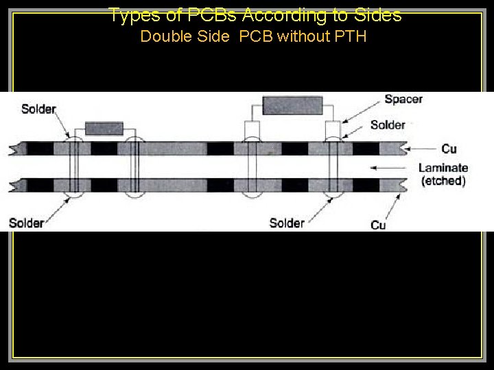
Types of PCBs According to Sides Double Side PCB without PTH

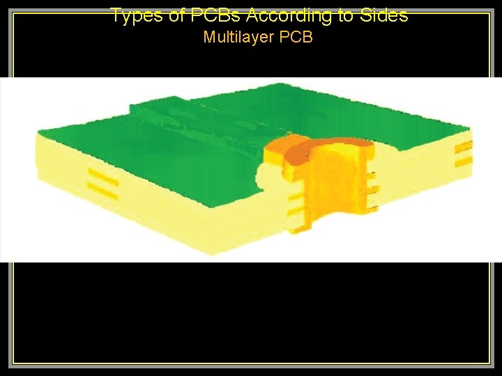
Types of PCBs According to Sides Multilayer PCB

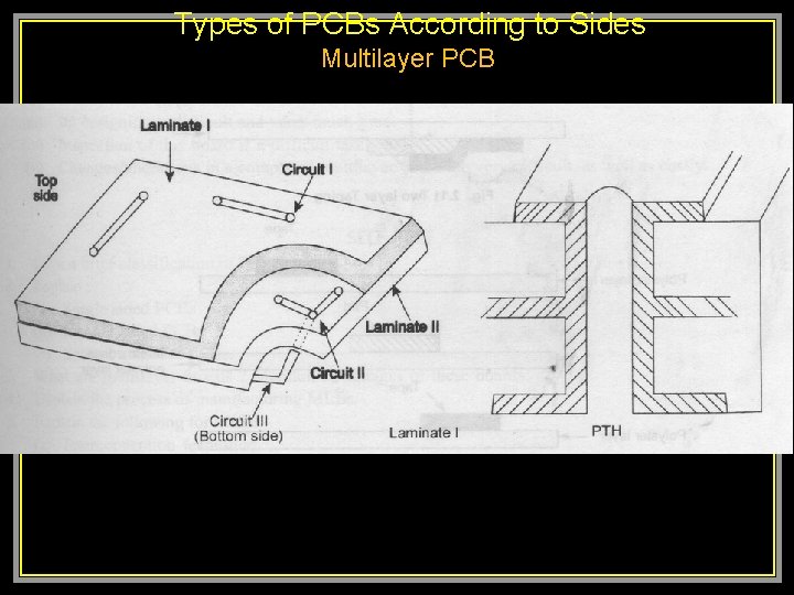
Types of PCBs According to Sides Multilayer PCB

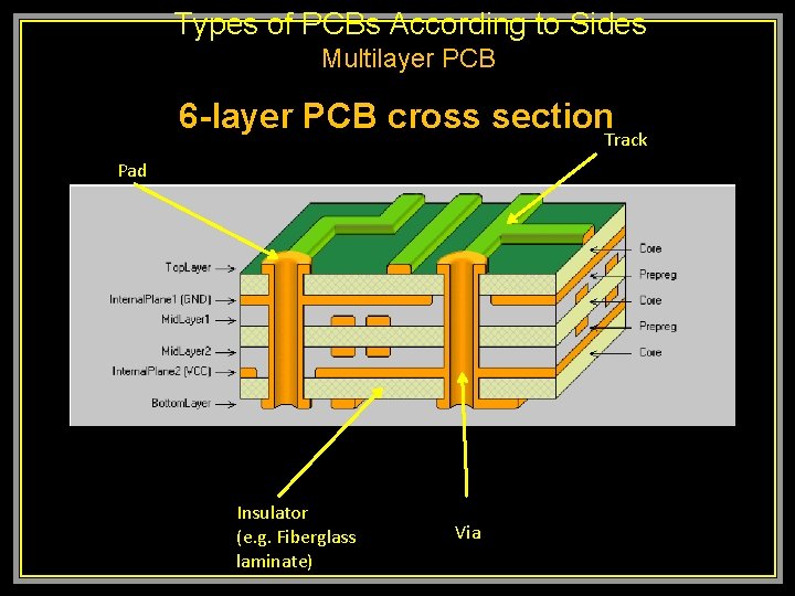
Types of PCBs According to Sides Multilayer PCB 6 -layer PCB cross section. Track Pad Insulator (e. g. Fiberglass laminate) Via

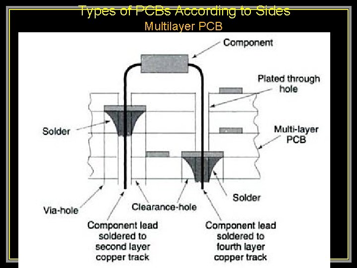
Types of PCBs According to Sides Multilayer PCB

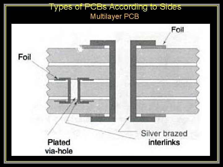
Types of PCBs According to Sides Multilayer PCB

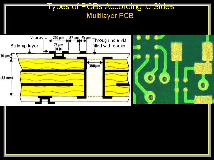
Types of PCBs According to Sides Multilayer PCB
![Classification of PCBs According to Base Material PTFE Polyamide Nylon Epoxy Resin Phenolic Classification of PCBs According to Base Material PTFE Polyamide [Nylon] Epoxy Resin Phenolic](https://slidetodoc.com/presentation_image/20bffd2e55099b24e907673326c21a24/image-27.jpg)
Classification of PCBs According to Base Material PTFE Polyamide [Nylon] Epoxy Resin Phenolic Resin Silicon Resin

Properties of Copper Clad Laminate • Electrical: (01) Volume Resistivity (02) Surface Resistivity (03) Dielectric Strength (04) Dielectric Constant (05) Dissipation Factor (06) Dielectric Loss (07) Loss Factor

Properties of Copper Clad Laminate • Mechanical: (01) Glass Transition Temperature (02) Flexural Strength (03) Peel Strength (04) Coefficient of Thermal Expansion (05) Water Absorption (06) Punchability (07) Bow and Twist

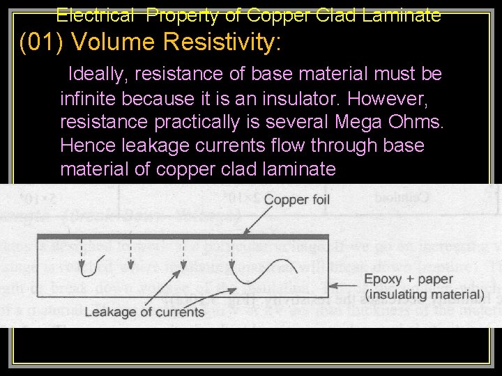
Electrical Property of Copper Clad Laminate (01) Volume Resistivity: Ideally, resistance of base material must be infinite because it is an insulator. However, resistance practically is several Mega Ohms. Hence leakage currents flow through base material of copper clad laminate
![Electrical Property of Copper Clad Laminate 01 Volume Resistivity continued The volume resistance is Electrical Property of Copper Clad Laminate (01) Volume Resistivity [continued]: The volume resistance is](https://slidetodoc.com/presentation_image/20bffd2e55099b24e907673326c21a24/image-31.jpg)
Electrical Property of Copper Clad Laminate (01) Volume Resistivity [continued]: The volume resistance is resistance offered to leakage current and can be written as Where, ρv = Volume resistivity in ohm-metre l = length of current path in metre A = Cross sectional area of the current path in m 2 perpendicular to direction of current

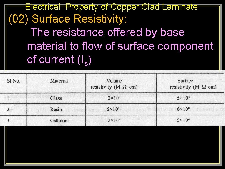
Electrical Property of Copper Clad Laminate (02) Surface Resistivity: The resistance offered by base material to flow of surface component of current (Is)

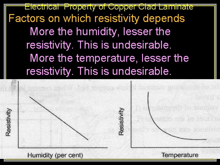
Electrical Property of Copper Clad Laminate Factors on which resistivity depends More the humidity, lesser the resistivity. This is undesirable. More the temperature, lesser the resistivity. This is undesirable.

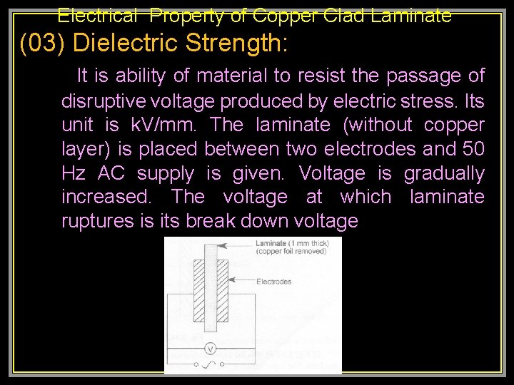
Electrical Property of Copper Clad Laminate (03) Dielectric Strength: It is ability of material to resist the passage of disruptive voltage produced by electric stress. Its unit is k. V/mm. The laminate (without copper layer) is placed between two electrodes and 50 Hz AC supply is given. Voltage is gradually increased. The voltage at which laminate ruptures is its break down voltage

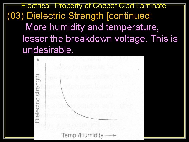
Electrical Property of Copper Clad Laminate (03) Dielectric Strength [continued: More humidity and temperature, lesser the breakdown voltage. This is undesirable.

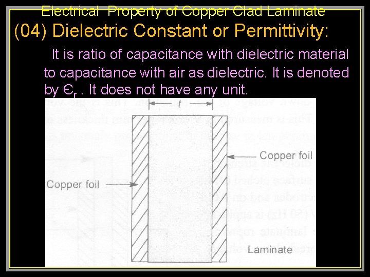
Electrical Property of Copper Clad Laminate (04) Dielectric Constant or Permittivity: It is ratio of capacitance with dielectric material to capacitance with air as dielectric. It is denoted by Єr. It does not have any unit.
![Electrical Property of Copper Clad Laminate 04 Dielectric Constant continued Lesser the value of Electrical Property of Copper Clad Laminate (04) Dielectric Constant [continued]: Lesser the value of](https://slidetodoc.com/presentation_image/20bffd2e55099b24e907673326c21a24/image-37.jpg)
Electrical Property of Copper Clad Laminate (04) Dielectric Constant [continued]: Lesser the value of dielectric constant, lesser will be dielectric loss

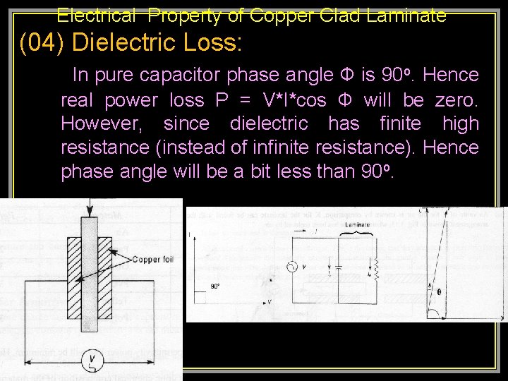
Electrical Property of Copper Clad Laminate (04) Dielectric Loss: In pure capacitor phase angle Ф is 90 o. Hence real power loss P = V*I*cos Ф will be zero. However, since dielectric has finite high resistance (instead of infinite resistance). Hence phase angle will be a bit less than 90 o.
![Electrical Property of Copper Clad Laminate 04 Dielectric Loss continued The dielectric loss is Electrical Property of Copper Clad Laminate (04) Dielectric Loss [continued]: The dielectric loss is](https://slidetodoc.com/presentation_image/20bffd2e55099b24e907673326c21a24/image-39.jpg)
Electrical Property of Copper Clad Laminate (04) Dielectric Loss [continued]: The dielectric loss is expressed as Where angle δ is known as ‘dielectric loss angle’. tan δ is known as Dissipation Factor of the insulator

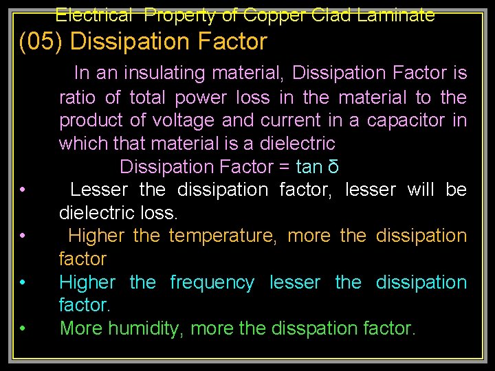
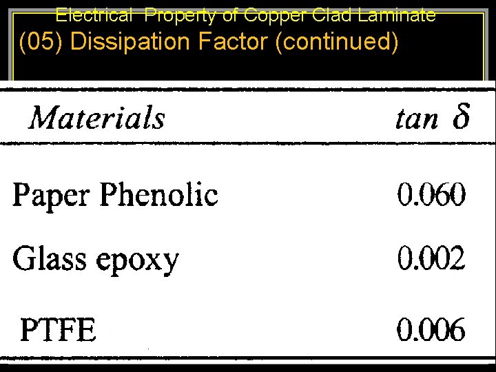
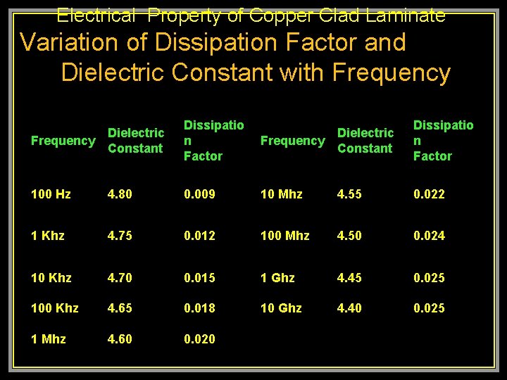
Electrical Property of Copper Clad Laminate (05) Dissipation Factor • • In an insulating material, Dissipation Factor is ratio of total power loss in the material to the product of voltage and current in a capacitor in which that material is a dielectric Dissipation Factor = tan δ Lesser the dissipation factor, lesser will be dielectric loss. Higher the temperature, more the dissipation factor Higher the frequency lesser the dissipation factor. More humidity, more the disspation factor.

Electrical Property of Copper Clad Laminate (05) Dissipation Factor (continued)

Electrical Property of Copper Clad Laminate Variation of Dissipation Factor and Dielectric Constant with Frequency Dielectric Frequency Constant Dissipatio n Factor 100 Hz 4. 80 0. 009 10 Mhz 4. 55 0. 022 1 Khz 4. 75 0. 012 100 Mhz 4. 50 0. 024 10 Khz 4. 70 0. 015 1 Ghz 4. 45 0. 025 100 Khz 4. 65 0. 018 10 Ghz 4. 40 0. 025 1 Mhz 4. 60 0. 020

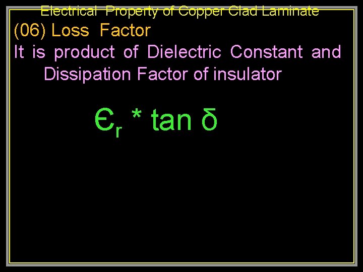
Electrical Property of Copper Clad Laminate (06) Loss Factor It is product of Dielectric Constant and Dissipation Factor of insulator Єr * tan δ

Electrical Properties of Copper Clad Laminates

Properties of Copper Clad Laminate • Mechanical: (01) Glass Transition Temperature (02) Flexural Strength (03) Peel Strength (04) Coefficient of Thermal Expansion (05) Water Absorption (06) Punchability (07) Bow and Twist

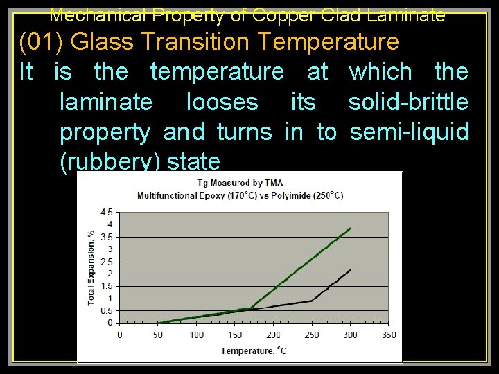
Mechanical Property of Copper Clad Laminate (01) Glass Transition Temperature It is the temperature at which the laminate looses its solid-brittle property and turns in to semi-liquid (rubbery) state

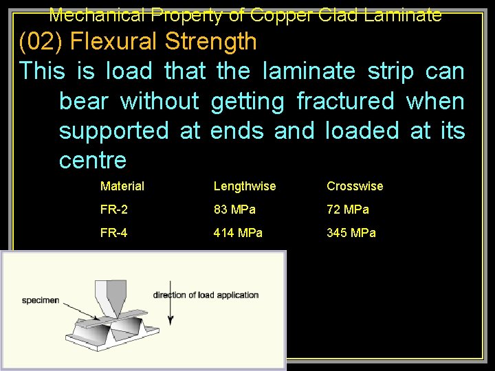
Mechanical Property of Copper Clad Laminate (02) Flexural Strength This is load that the laminate strip can bear without getting fractured when supported at ends and loaded at its centre Material Lengthwise Crosswise FR-2 83 MPa 72 MPa FR-4 414 MPa 345 MPa

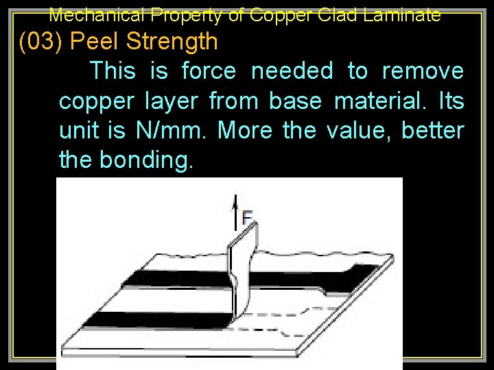
Mechanical Property of Copper Clad Laminate (03) Peel Strength This is force needed to remove copper layer from base material. Its unit is N/mm. More the value, better the bonding.

Mechanical Property of Copper Clad Laminate (04) Coefficient of Thermal Expansion CTE More the heat, laminate length increases. With lower temperature, its length decreases. CTE is measured in mm/o. C per metre. Epoxy Resin has high CTE 35 to 45 Fibreglass has low CTE 5 to 6

Mechanical Property of Copper Clad Laminate (05) Water Absorption It is defined as the ratio of weight of water absorbed to weight of dry laminate. More water absorption, more will be the weight of the laminate

Mechanical Property of Copper Clad Laminate (06) Punchability The PCB is drilled / punched for mounting components. A hole should have smooth edges, smooth from its inside and without cracks. For this, the laminate must be soft and free from warp and twist

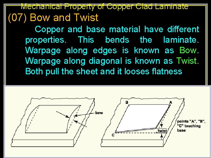
Mechanical Property of Copper Clad Laminate (07) Bow and Twist Copper and base material have different properties. This bends the laminate. Warpage along edges is known as Bow. Warpage along diagonal is known as Twist. Both pull the sheet and it looses flatness

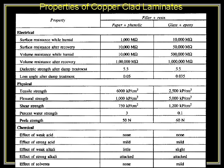
Properties of Copper Clad Laminates

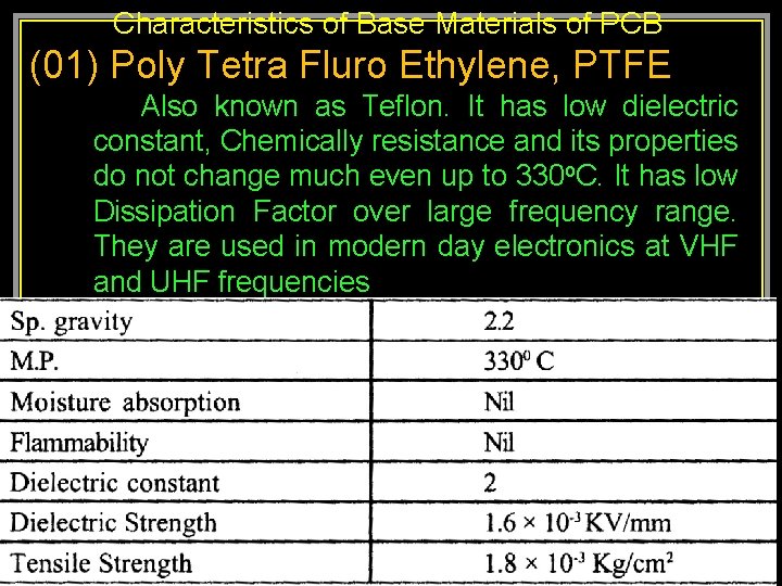
Characteristics of Base Materials of PCB (01) Poly Tetra Fluro Ethylene, PTFE Also known as Teflon. It has low dielectric constant, Chemically resistance and its properties do not change much even up to 330 o. C. It has low Dissipation Factor over large frequency range. They are used in modern day electronics at VHF and UHF frequencies
![Characteristics of Base Materials of PCB 02 Polyamide Resin Nylon They have good mechanical Characteristics of Base Materials of PCB (02) Polyamide Resin [Nylon] They have good mechanical](https://slidetodoc.com/presentation_image/20bffd2e55099b24e907673326c21a24/image-55.jpg)
Characteristics of Base Materials of PCB (02) Polyamide Resin [Nylon] They have good mechanical properties, High volume and surface resistivities, and good dielectric strength. They are heat resistant. Copper binding strength is high. They are used in multilayer PCBs.

Characteristics of Base Materials of PCB (03) Epoxy Resin They have high resistivity. Low shrinkage, strong adhesion, low water absorption. Epoxy resin combined with glass forms base material for PCB. These have good mechanical and electrical properties.

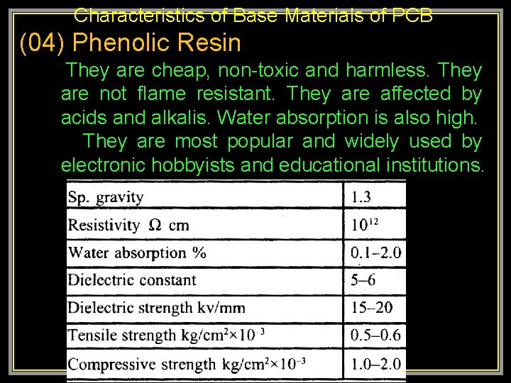
Characteristics of Base Materials of PCB (04) Phenolic Resin They are cheap, non-toxic and harmless. They are not flame resistant. They are affected by acids and alkalis. Water absorption is also high. They are most popular and widely used by electronic hobbyists and educational institutions.

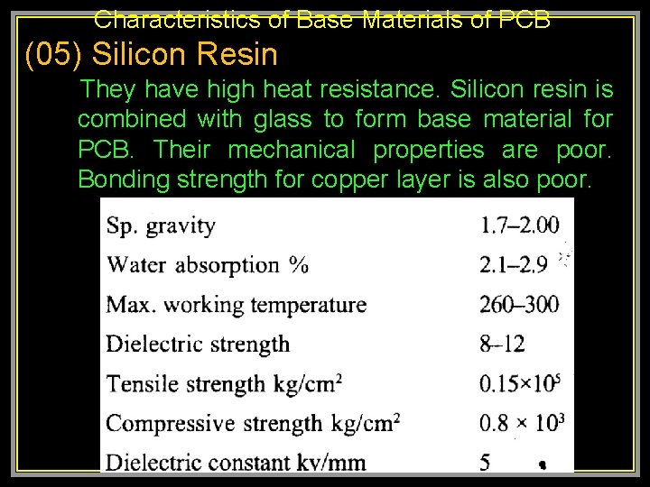
Characteristics of Base Materials of PCB (05) Silicon Resin They have high heat resistance. Silicon resin is combined with glass to form base material for PCB. Their mechanical properties are poor. Bonding strength for copper layer is also poor.

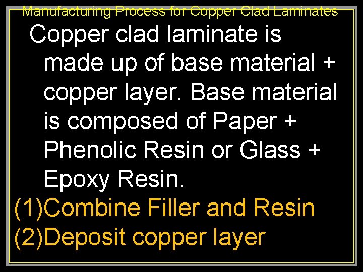
Manufacturing Process for Copper Clad Laminates Copper clad laminate is made up of base material + copper layer. Base material is composed of Paper + Phenolic Resin or Glass + Epoxy Resin. (1)Combine Filler and Resin (2)Deposit copper layer

Manufacturing Process for Copper Clad Laminates

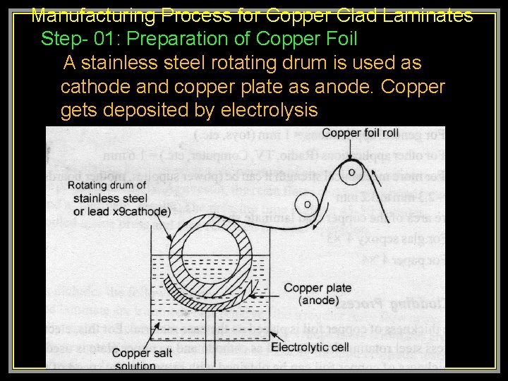
Manufacturing Process for Copper Clad Laminates Step- 01: Preparation of Copper Foil A stainless steel rotating drum is used as cathode and copper plate as anode. Copper gets deposited by electrolysis

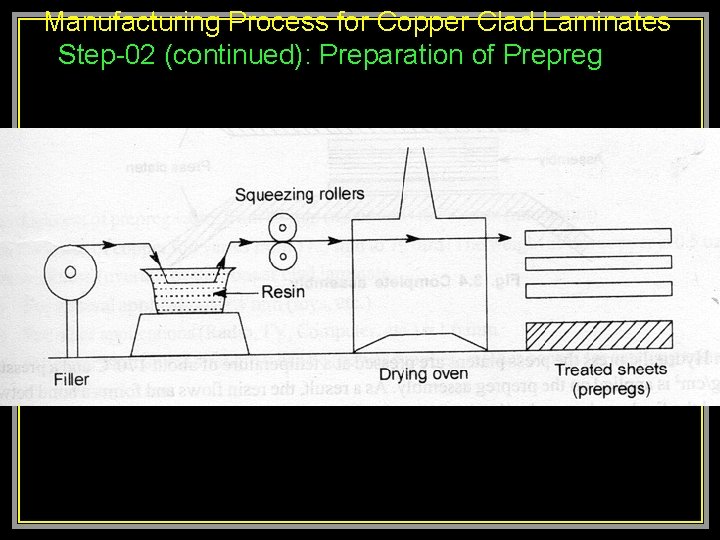
Manufacturing Process for Copper Clad Laminates Step-02: Preparation of Prepreg (a) The filler (e. g. paper) is coated with resin (b) This material passes through squeeze rollers and through drying oven. The resin gets polymerized. This is known as Prepreg (c) The prepreg is stored in room at 70 o. C at 35% humidity Paper + Phenolic Resin gives prepreg for paper phenolic base material Glass cloth + Epoxy Resin gives prepreg for paper phenolic base material

Manufacturing Process for Copper Clad Laminates Step-02 (continued): Preparation of Prepreg

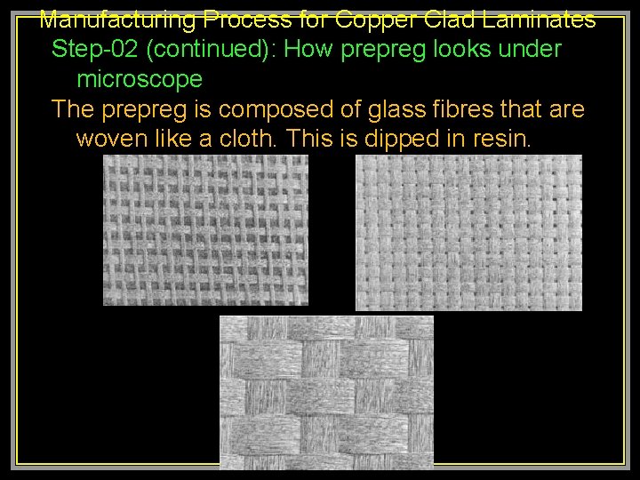
Manufacturing Process for Copper Clad Laminates Step-02 (continued): How prepreg looks under microscope The prepreg is composed of glass fibres that are woven like a cloth. This is dipped in resin.

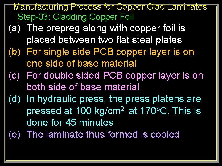
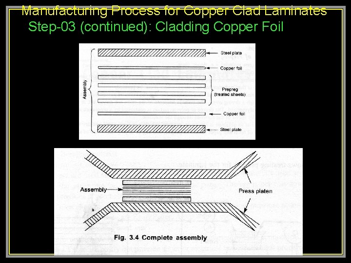
Manufacturing Process for Copper Clad Laminates Step-03: Cladding Copper Foil (a) The prepreg along with copper foil is placed between two flat steel plates (b) For single side PCB copper layer is on one side of base material (c) For double sided PCB copper layer is on both side of base material (d) In hydraulic press, the press platens are pressed at 100 kg/cm 2 at 170 o. C. This is done for 45 minutes (e) The laminate thus formed is cooled

Manufacturing Process for Copper Clad Laminates Step-03 (continued): Cladding Copper Foil

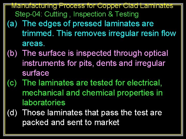
Manufacturing Process for Copper Clad Laminates Step-04: Cutting , Inspection & Testing (a) The edges of pressed laminates are trimmed. This removes irregular resin flow areas. (b) The surface is inspected through optical instruments for pits, dents and irregular surface (c) The laminates are tested for electrical, mechanical and chemical properties in laboratories (d) Those laminates that pass the test are packed and sent to market