Power Point for Optoelectronics and Photonics Principles and




- Slides: 50

Power Point for Optoelectronics and Photonics: Principles and Practices Second Edition A Complete Course in Power Point Chapter 5 ISBN-10: 0133081753 Second Edition Version 1. 014 [19 January 2013]

Updates and Corrected Slides Class Demonstrations Class Problems Check author’s website http: //optoelectronics. usask. ca Email errors and corrections to safa. kasap@yahoo. com

Slides on Selected Topics on Optoelectronics may be available at the author website http: //optoelectronics. usask. ca Email errors and corrections to safa. kasap@yahoo. com

Copyright Information and Permission: Part I This Power Point presentation is a copyrighted supplemental material to the textbook Optoelectronics and Photonics: Principles & Practices, Second Edition, S. O. Kasap, Pearson Education (USA), ISBN-10: 0132151499, ISBN-13: 9780132151498. © 2013 Pearson Education. Permission is given to instructors to use these Power Point slides in their lectures provided that the above book has been adopted as a primary required textbook for the course. Slides may be used in research seminars at research meetings, symposia and conferences provided that the author, book title, and copyright information are clearly displayed under each figure. It is unlawful to use the slides for teaching if the textbook is not a required primary book for the course. The slides cannot be distributed in any form whatsoever, especially on the internet, without the written permission of Pearson Education. Please report typos and errors directly to the author: safa. kasap@yahoo. com

PEARSON Copyright Information and Permission: Part II This Power Point presentation is a copyrighted supplemental material to the textbook Optoelectronics and Photonics: Principles & Practices, Second Edition, S. O. Kasap, Pearson Education (USA), ISBN-10: 0132151499, ISBN-13: 9780132151498. © 2013 Pearson Education. The slides cannot be distributed in any form whatsoever, electronically or in print form, without the written permission of Pearson Education. It is unlawful to post these slides, or part of a slide or slides, on the internet. Copyright © 2013, 2001 by Pearson Education, Inc. , Upper Saddle River, New Jersey, 07458. All rights reserved. Printed in the United States of America. This publication is protected by Copyright and permission should be obtained from the publisher prior to any prohibited reproduction, storage in a retrieval system, or transmission in any form or by any means, electronic, mechanical, photocopying, recording, or likewise. For information regarding permission(s), write to: Rights and Permissions Department.

Important Note You may use color illustrations from this Power Point in your research-related seminars or research-related presentations at scientific or technical meetings, symposia or conferences provided that you fully cite the following reference under each figure From: S. O. Kasap, Optoelectronics and Photonics: Principles and Practices, Second Edition, © 2013 Pearson Education, USA

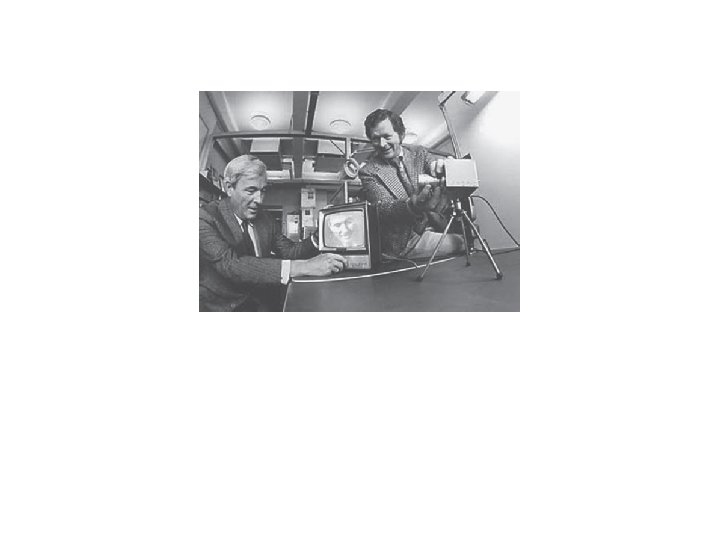
Chapter 5 Photodetectors and Image Sensors The inventors of the CCD (charge coupled device) image sensor at AT&T Bell Labs: Willard Boyle (left) and George Smith (right). The CCD was invented in 1969, the first CCD solid state camera was demonstrated in 1970, and a broadcast quality TV camera by 1975. (W. S. Boyle and G. E. Smith, “Charge Coupled Semiconductor Devices", Bell Systems Technical Journal, 49, 587, 1970. (Courtesy of Alcatel-Lucent Bell Labs. )

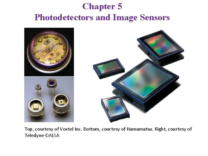
Chapter 5 Photodetectors and Image Sensors Top, courtesy of Voxtel Inc. Bottom, courtesy of Hamamatsu. Right, courtesy of Teledyne-DALSA

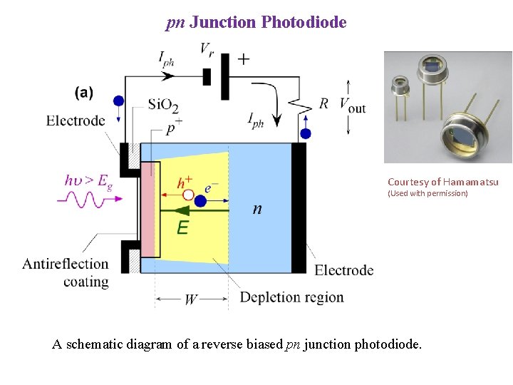
pn Junction Photodiode Courtesy of Hamamatsu (Used with permission) A schematic diagram of a reverse biased pn junction photodiode.

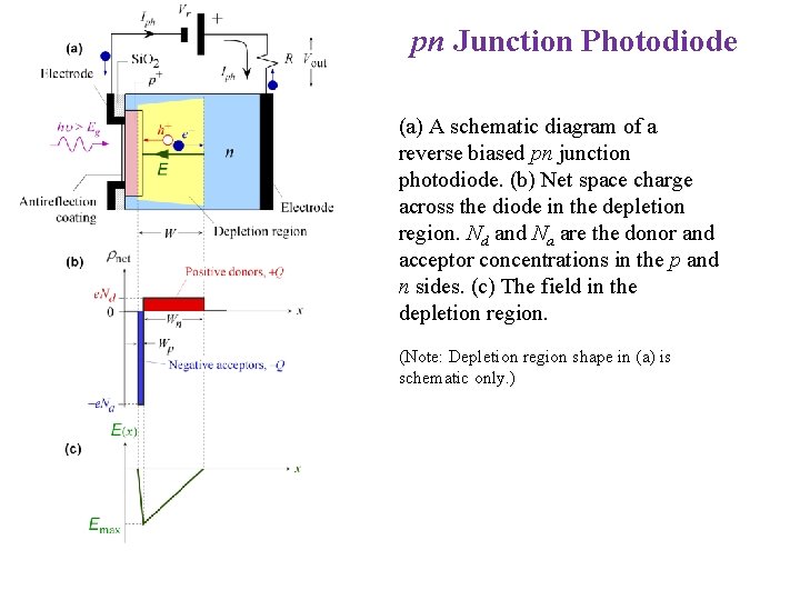
pn Junction Photodiode (a) A schematic diagram of a reverse biased pn junction photodiode. (b) Net space charge across the diode in the depletion region. Nd and Na are the donor and acceptor concentrations in the p and n sides. (c) The field in the depletion region. (Note: Depletion region shape in (a) is schematic only. )

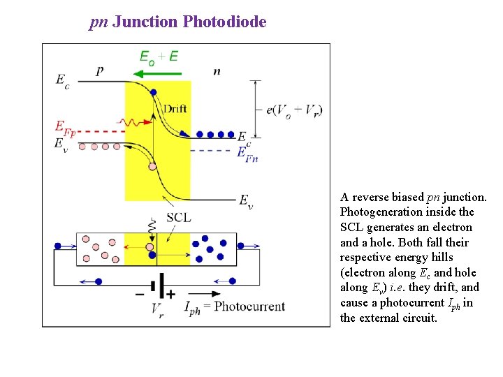
pn Junction Photodiode A reverse biased pn junction. Photogeneration inside the SCL generates an electron and a hole. Both fall their respective energy hills (electron along Ec and hole along Ev) i. e. they drift, and cause a photocurrent Iph in the external circuit.

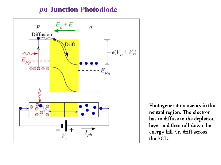
pn Junction Photodiode Photogeneration occurs in the neutral region. The electron has to diffuse to the depletion layer and then roll down the energy hill i. e. drift across the SCL.

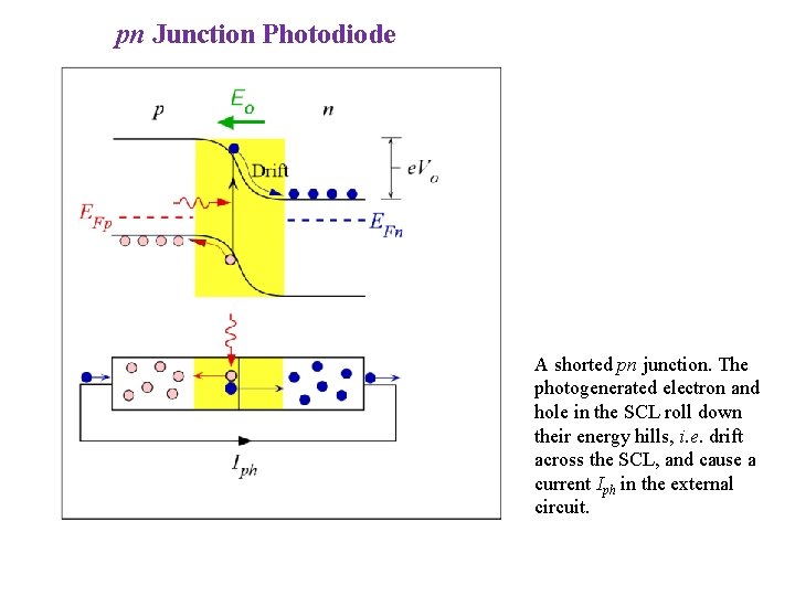
pn Junction Photodiode A shorted pn junction. The photogenerated electron and hole in the SCL roll down their energy hills, i. e. drift across the SCL, and cause a current Iph in the external circuit.

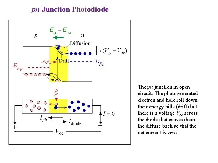
pn Junction Photodiode The pn junction in open circuit. The photogenerated electron and hole roll down their energy hills (drift) but there is a voltage Voc across the diode that causes them the diffuse back so that the net current is zero.

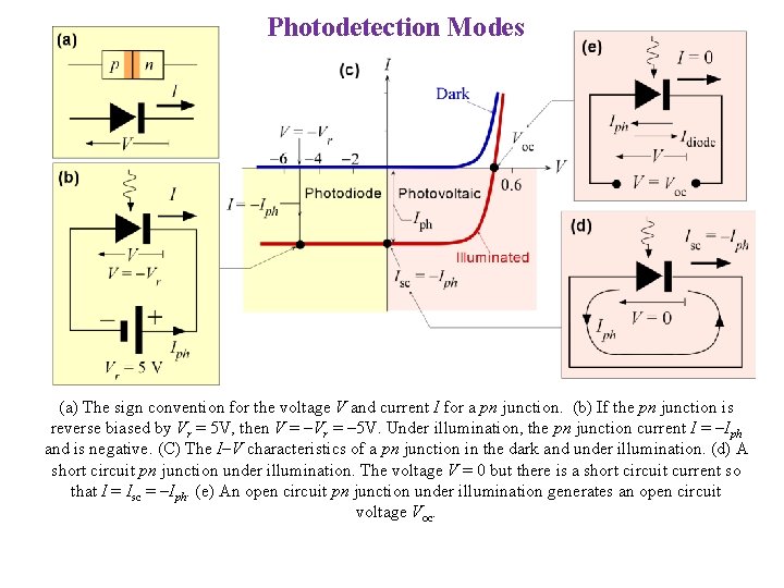
Photodetection Modes (a) The sign convention for the voltage V and current I for a pn junction. (b) If the pn junction is reverse biased by Vr = 5 V, then V = Vr = 5 V. Under illumination, the pn junction current I = Iph and is negative. (C) The I V characteristics of a pn junction in the dark and under illumination. (d) A short circuit pn junction under illumination. The voltage V = 0 but there is a short circuit current so that I = Isc = Iph. (e) An open circuit pn junction under illumination generates an open circuit voltage Voc.

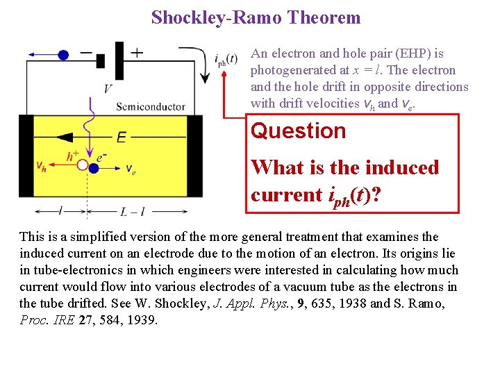
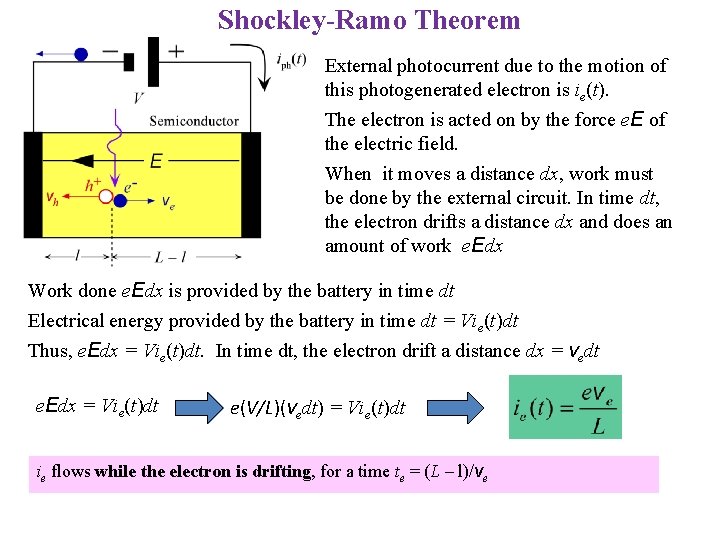
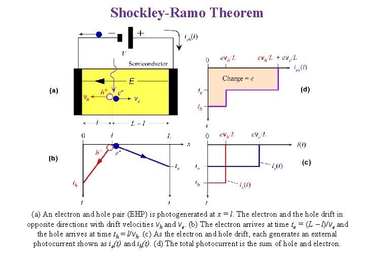
Shockley-Ramo Theorem An electron and hole pair (EHP) is photogenerated at x = l. The electron and the hole drift in opposite directions with drift velocities vh and ve. Question What is the induced current iph(t)? This is a simplified version of the more general treatment that examines the induced current on an electrode due to the motion of an electron. Its origins lie in tube-electronics in which engineers were interested in calculating how much current would flow into various electrodes of a vacuum tube as the electrons in the tube drifted. See W. Shockley, J. Appl. Phys. , 9, 635, 1938 and S. Ramo, Proc. IRE 27, 584, 1939.

Shockley-Ramo Theorem External photocurrent due to the motion of this photogenerated electron is ie(t). The electron is acted on by the force e. E of the electric field. When it moves a distance dx, work must be done by the external circuit. In time dt, the electron drifts a distance dx and does an amount of work e. Edx Work done e. Edx is provided by the battery in time dt Electrical energy provided by the battery in time dt = Vie(t)dt Thus, e. Edx = Vie(t)dt. In time dt, the electron drift a distance dx = vedt e. Edx = Vie(t)dt e(V/L)(vedt) = Vie(t)dt ie flows while the electron is drifting, for a time te = (L – l)/ve

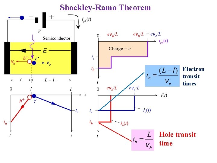
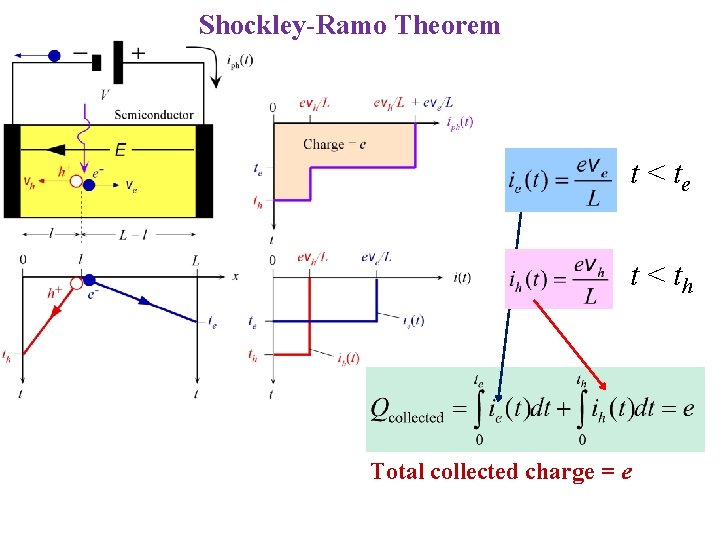
Shockley-Ramo Theorem (a) An electron and hole pair (EHP) is photogenerated at x = l. The electron and the hole drift in opposite directions with drift velocities vh and ve. (b) The electron arrives at time te = (L - l)/ve and the hole arrives at time th = l/vh. (c) As the electron and hole drift, each generates an external photocurrent shown as ie(t) and ih(t). (d) The total photocurrent is the sum of hole and electron.

Shockley-Ramo Theorem Electron transit times Hole transit time

Shockley-Ramo Theorem t < te t < th Total collected charge = e

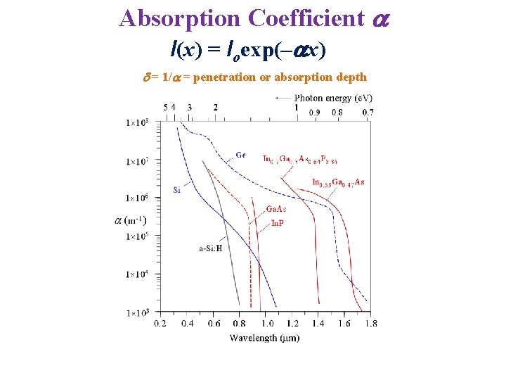
Absorption Coefficient a I(x) = Ioexp(–ax) d = 1/a = penetration or absorption depth

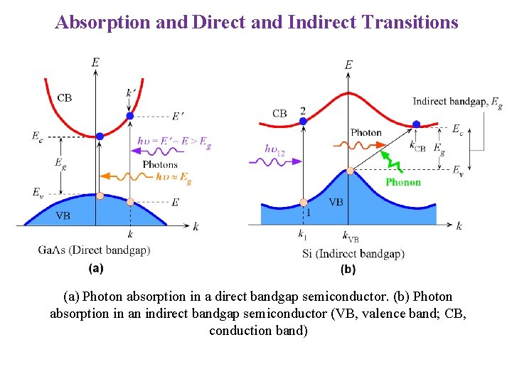
Absorption and Direct and Indirect Transitions (a) Photon absorption in a direct bandgap semiconductor. (b) Photon absorption in an indirect bandgap semiconductor (VB, valence band; CB, conduction band)

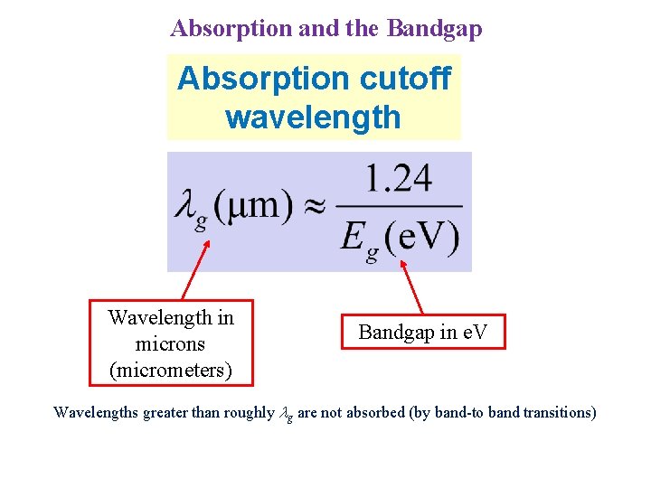
Absorption and the Bandgap Absorption cutoff wavelength Wavelength in microns (micrometers) Bandgap in e. V Wavelengths greater than roughly g are not absorbed (by band-to band transitions)

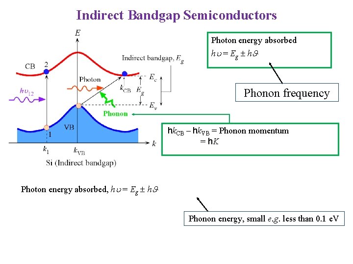
Indirect Bandgap Semiconductors Photon energy absorbed hu = Eg h Phonon frequency hk. CB – hk. VB = Phonon momentum = h. K Photon energy absorbed, hu = Eg h Phonon energy, small e. g. less than 0. 1 e. V

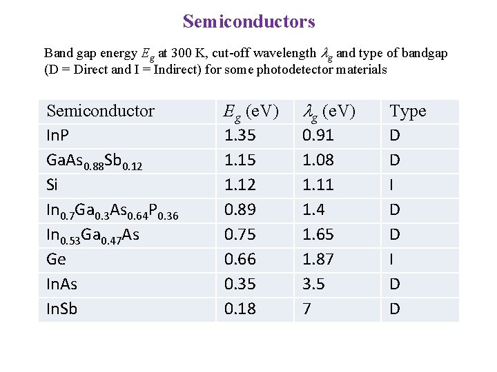
Semiconductors Band gap energy Eg at 300 K, cut-off wavelength g and type of bandgap (D = Direct and I = Indirect) for some photodetector materials Semiconductor In. P Ga. As 0. 88 Sb 0. 12 Si In 0. 7 Ga 0. 3 As 0. 64 P 0. 36 In 0. 53 Ga 0. 47 As Ge In. As In. Sb Eg (e. V) 1. 35 1. 12 0. 89 0. 75 0. 66 0. 35 0. 18 g (e. V) 0. 91 1. 08 1. 11 1. 4 1. 65 1. 87 3. 5 7 Type D D I D D

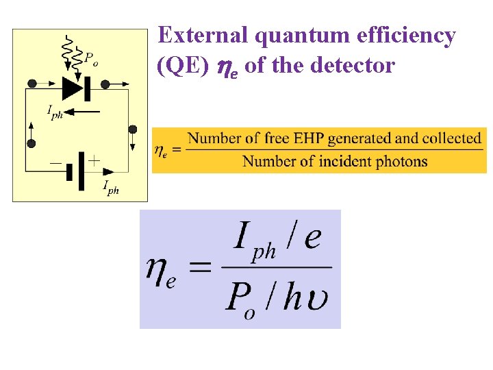
External quantum efficiency (QE) he of the detector

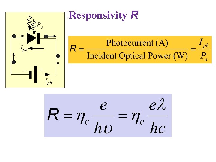
Responsivity R

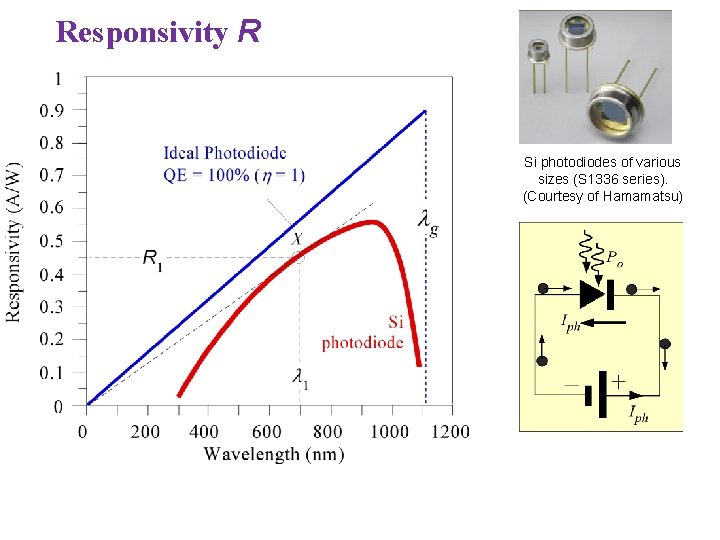
Responsivity R Si photodiodes of various sizes (S 1336 series). (Courtesy of Hamamatsu)

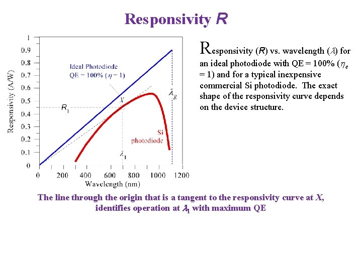
Responsivity R Responsivity (R) vs. wavelength ( ) for an ideal photodiode with QE = 100% (he = 1) and for a typical inexpensive commercial Si photodiode. The exact shape of the responsivity curve depends on the device structure. The line through the origin that is a tangent to the responsivity curve at X, identifies operation at l 1 with maximum QE

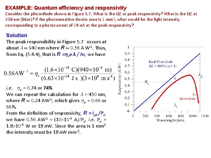
EXAMPLE: Quantum efficiency and responsivity Consider the photodiode shown in Figure 5. 7. What is the QE at peak responsivity? What is the QE at 450 nm (blue)? If the photosensitive device area is 1 mm 2, what would be the light intensity corresponding to a photocurrent of 10 n. A at the peak responsivity? Solution The peak responsibility in Figure 5. 7 occurs at about 940 nm where R 0. 56 A W-1. Thus, from Eq. (5. 4. 4), that is R =heel / hc, we have i. e. he = 0. 74 or 74% We can repeat the calculation for = 450 nm, where R 0. 24 AW-1, which gives he = 0. 66 or 66%. From the definition of responsivity, R = Iph /Po, we have 0. 56 AW-1 = (10× 10 -9 A)/Po, i. e. Po = 1. 8× 10 -8 W or 18 n. W. Since the area is 1 mm 2 the intensity must be 18 n. W mm-2.

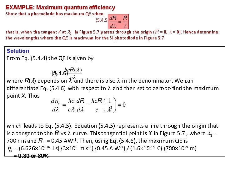
EXAMPLE: Maximum quantum efficiency Show that a photodiode has maximum QE when (5. 4. 5) that is, when the tangent X at 1 in Figure 5. 7 passes through the origin (R = 0, = 0). Hence determine the wavelengths where the QE is maximum for the Si photodiode in Figure 5. 7 Solution From Eq. (5. 4. 4) the QE is given by (5. 4. 6) where R( ) depends on l and there is also l in the denominator. We can differentiate Eq. (5. 4. 6) with respect to l and then set to zero to find the maximum point X. Thus which leads to Eq. (5. 4. 5). Equation (5. 4. 5) represents a line through the origin that is a tangent to the R vs l curve. This tangential point is X in Figure 5. 7 , where 1 = 700 nm and R 1 = 0. 45 AW-1. Then, using Eq. (5. 4. 6), the maximum QE is he = (6. 626× 10 -34 J s) (3× 10⁸ m s-1) (0. 45 A W-1) / (1. 6× 10 -19 C) (700× 10 -9 m) = 0. 80 or 80%

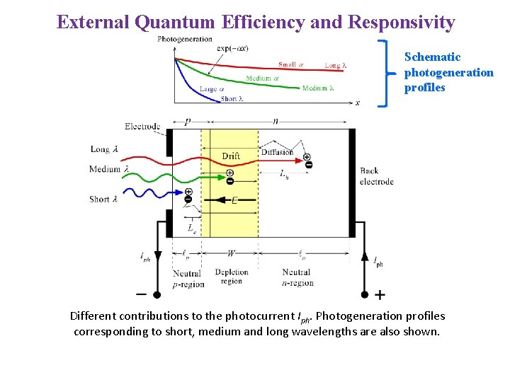
External Quantum Efficiency and Responsivity Schematic photogeneration profiles Different contributions to the photocurrent Iph. Photogeneration profiles corresponding to short, medium and long wavelengths are also shown.

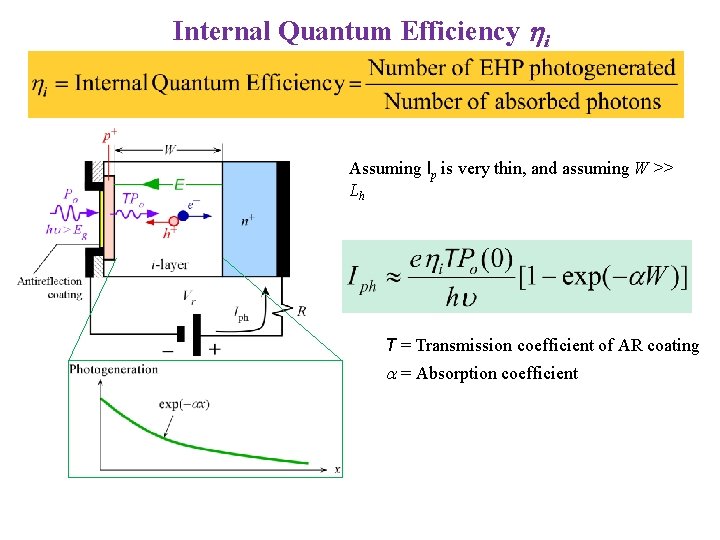
Internal Quantum Efficiency hi Assuming lp is very thin, and assuming W >> Lh T = Transmission coefficient of AR coating a = Absorption coefficient

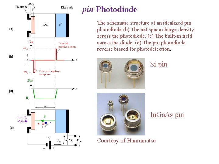
pin Photodiode The schematic structure of an idealized pin photodiode (b) The net space charge density across the photodiode. (c) The built-in field across the diode. (d) The pin photodiode reverse biased for photodetection. Si pin In. Ga. As pin Courtesy of Hamamatsu

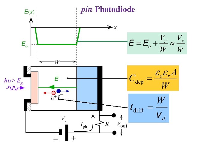
pin Photodiode

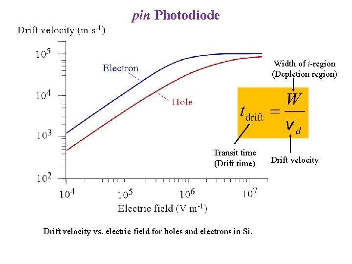
pin Photodiode Width of i-region (Depletion region) Transit time (Drift time) Drift velocity vs. electric field for holes and electrons in Si. Drift velocity

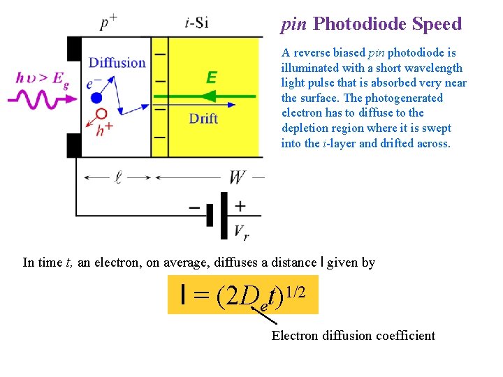
pin Photodiode Speed A reverse biased pin photodiode is illuminated with a short wavelength light pulse that is absorbed very near the surface. The photogenerated electron has to diffuse to the depletion region where it is swept into the i-layer and drifted across. In time t, an electron, on average, diffuses a distance l given by l = (2 Det)1/2 Electron diffusion coefficient

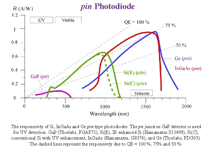
pin Photodiode The responsivity of Si, In. Ga. As and Ge pin type photodiodes. The pn junction Ga. P detector is used for UV detection. Ga. P (Thorlabs, FGAP 71), Si(E), IR enhanced Si (Hamamatsu S 11499), Si(C), conventional Si with UV enhancement, In. Ga. As (Hamamatsu, G 8376), and Ge (Thorlabs, FDG 03). The dashed lines represent the responsivity due to QE = 100 %, 75% and 50 %.

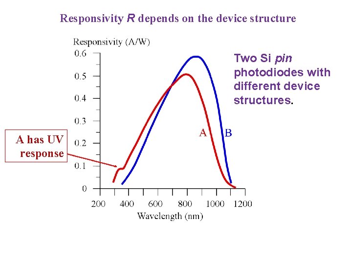
Responsivity R depends on the device structure Two Si pin photodiodes with different device structures. A has UV response

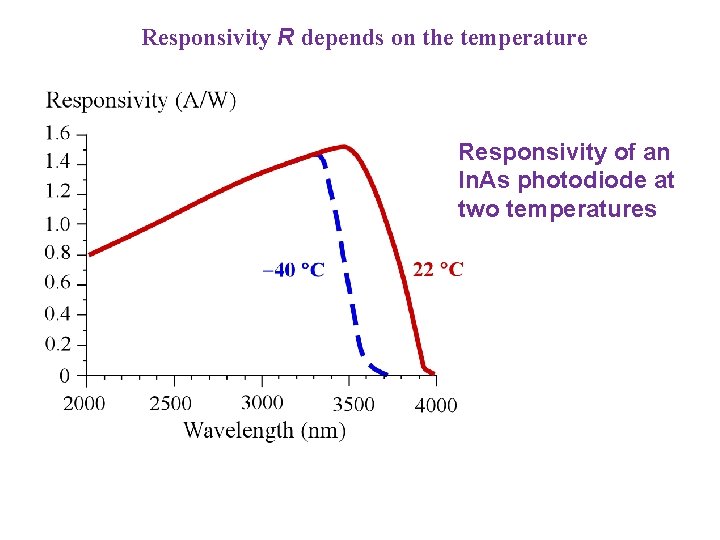
Responsivity R depends on the temperature Responsivity of an In. As photodiode at two temperatures

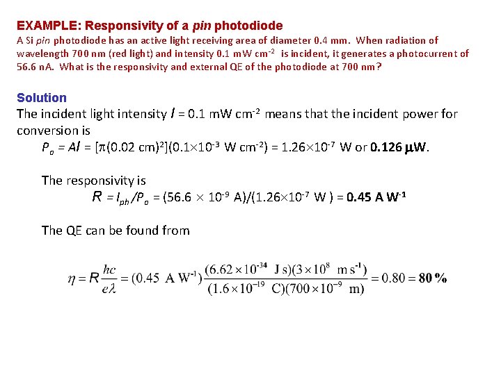
EXAMPLE: Responsivity of a pin photodiode A Si pin photodiode has an active light receiving area of diameter 0. 4 mm. When radiation of wavelength 700 nm (red light) and intensity 0. 1 m. W cm-2 is incident, it generates a photocurrent of 56. 6 n. A. What is the responsivity and external QE of the photodiode at 700 nm? Solution The incident light intensity I = 0. 1 m. W cm-2 means that the incident power for conversion is Po = AI = [ (0. 02 cm)2](0. 1 10 -3 W cm-2) = 1. 26 10 -7 W or 0. 126 m. W. The responsivity is R = Iph /Po = (56. 6 10 -9 A)/(1. 26 10 -7 W ) = 0. 45 A W-1 The QE can be found from

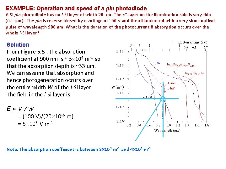
EXAMPLE: Operation and speed of a pin photodiode A Si pin photodiode has an i-Si layer of width 20 mm. The p+-layer on the illumination side is very thin (0. 1 mm). The pin is reverse biased by a voltage of 100 V and then illuminated with a very short optical pulse of wavelength 900 nm. What is the duration of the photocurrent if absorption occurs over the whole i-Si layer? Solution From Figure 5. 5 , the absorption coefficient at 900 nm is ~ 3 104 m-1 so that the absorption depth is ~33 mm. We can assume that absorption and hence photogeneration occurs over the entire width W of the i-Si layer. The field in the i-Si layer is E Vr / W = (100 V)/(20 10 -6 m) = 5 106 V m-1 Note: The absorption coefficient is between 3 104 m-1 and 4 104 m-1

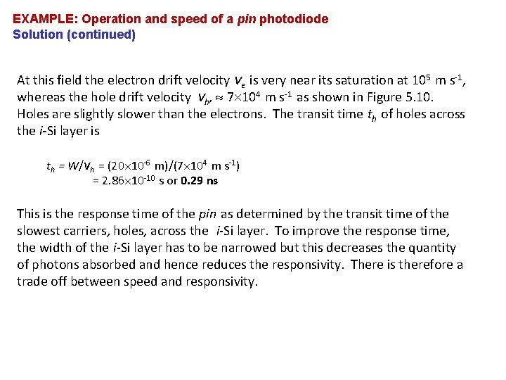
EXAMPLE: Operation and speed of a pin photodiode Solution (continued) At this field the electron drift velocity ve is very near its saturation at 105 m s-1, whereas the hole drift velocity vh, 7 104 m s-1 as shown in Figure 5. 10. Holes are slightly slower than the electrons. The transit time th of holes across the i-Si layer is th = W/vh = (20 10 -6 m)/(7 104 m s-1) = 2. 86 10 -10 s or 0. 29 ns This is the response time of the pin as determined by the transit time of the slowest carriers, holes, across the i-Si layer. To improve the response time, the width of the i-Si layer has to be narrowed but this decreases the quantity of photons absorbed and hence reduces the responsivity. There is therefore a trade off between speed and responsivity.

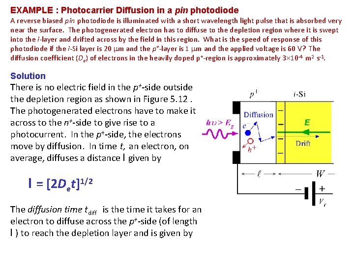
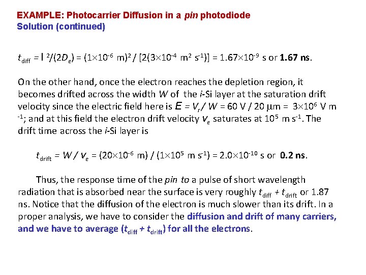
EXAMPLE : Photocarrier Diffusion in a pin photodiode A reverse biased pin photodiode is illuminated with a short wavelength light pulse that is absorbed very near the surface. The photogenerated electron has to diffuse to the depletion region where it is swept into the i-layer and drifted across by the field in this region. What is the speed of response of this photodiode if the i-Si layer is 20 mm and the p+-layer is 1 mm and the applied voltage is 60 V? The diffusion coefficient (De) of electrons in the heavily doped p+-region is approximately 3 10 -4 m 2 s-1. Solution There is no electric field in the p+-side outside the depletion region as shown in Figure 5. 12. The photogenerated electrons have to make it across to the n+-side to give rise to a photocurrent. In the p+-side, the electrons move by diffusion. In time t, an electron, on average, diffuses a distance l given by l = [2 Det]1/2 The diffusion time tdiff is the time it takes for an electron to diffuse across the p+-side (of length l ) to reach the depletion layer and is given by

EXAMPLE: Photocarrier Diffusion in a pin photodiode Solution (continued) tdiff = l 2/(2 De) = (1 10 -6 m)2 / [2(3 10 -4 m 2 s-1)] = 1. 67 10 -9 s or 1. 67 ns. On the other hand, once the electron reaches the depletion region, it becomes drifted across the width W of the i-Si layer at the saturation drift velocity since the electric field here is E = Vr / W = 60 V / 20 mm = 3 106 V m -1; and at this field the electron drift velocity v saturates at 105 m s-1. The e drift time across the i-Si layer is tdrift = W / ve = (20 10 -6 m) / (1 105 m s-1) = 2. 0 10 -10 s or 0. 2 ns. Thus, the response time of the pin to a pulse of short wavelength radiation that is absorbed near the surface is very roughly tdiff + tdrift or 1. 87 ns. Notice that the diffusion of the electron is much slower than its drift. In a proper analysis, we have to consider the diffusion and drift of many carriers, and we have to average (tdiff + tdrift) for all the electrons.

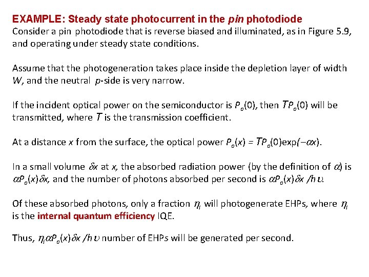
EXAMPLE: Steady state photocurrent in the pin photodiode Consider a pin photodiode that is reverse biased and illuminated, as in Figure 5. 9, and operating under steady state conditions. Assume that the photogeneration takes place inside the depletion layer of width W, and the neutral p-side is very narrow. If the incident optical power on the semiconductor is Po(0), then TPo(0) will be transmitted, where T is the transmission coefficient. At a distance x from the surface, the optical power Po(x) = TPo(0)exp(-ax). In a small volume dx at x, the absorbed radiation power (by the definition of a) is a. Po(x)dx, and the number of photons absorbed per second is a. Po(x)dx /hu. Of these absorbed photons, only a fraction hi will photogenerate EHPs, where hi is the internal quantum efficiency IQE. Thus, hia. Po(x)dx /hu number of EHPs will be generated per second.

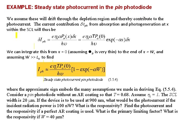
EXAMPLE: Steady state photocurrent in the pin photodiode We assume these will drift through the depletion region and thereby contribute to the photocurrent. The current contribution d Iph from absorption and photogeneration at x within the SCL will thus be We can integrate this from x = 0 (assuming lp is very thin) to the end of x = W, and assuming W >> Lh to find Steady state photocurrent pin photodiode (5. 5. 4) where the approximate sign embeds the many assumptions we made in deriving Eq. (5. 5. 4). Consider a pin photodiode without an AR coating so that T = 0. 68. Assume hi = 1. The SCL width is 20 mm. If the device is to be used at 900 nm, what would be the photocurrent if the incident radiation power is 100 n. W? What is the responsivity? Find the photocurrent and the responsivity if a perfect AR coating is used. What is the primary limiting factor? What is the responsivity if W = 40 µm?

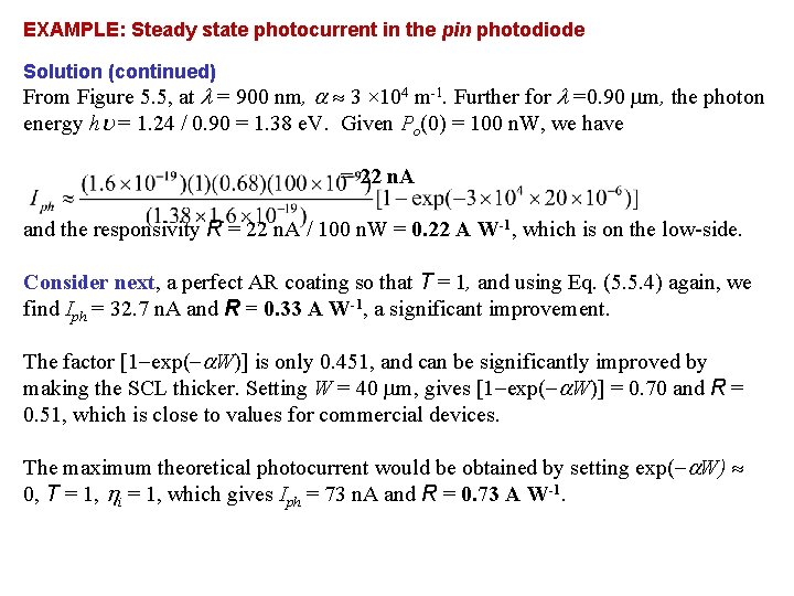
EXAMPLE: Steady state photocurrent in the pin photodiode Solution (continued) From Figure 5. 5, at = 900 nm, a 3 × 10⁴ m-1. Further for =0. 90 mm, the photon energy hu = 1. 24 / 0. 90 = 1. 38 e. V. Given Po(0) = 100 n. W, we have = 22 n. A and the responsivity R = 22 n. A / 100 n. W = 0. 22 A W-1, which is on the low-side. Consider next, a perfect AR coating so that T = 1, and using Eq. (5. 5. 4) again, we find Iph = 32. 7 n. A and R = 0. 33 A W-1, a significant improvement. The factor [1 exp( a. W)] is only 0. 451, and can be significantly improved by making the SCL thicker. Setting W = 40 mm, gives [1 exp( a. W)] = 0. 70 and R = 0. 51, which is close to values for commercial devices. The maximum theoretical photocurrent would be obtained by setting exp( a. W) 0, T = 1, hi = 1, which gives Iph = 73 n. A and R = 0. 73 A W-1.

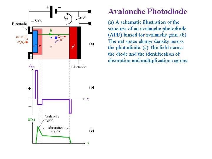
Avalanche Photodiode (a) A schematic illustration of the structure of an avalanche photodiode (APD) biased for avalanche gain. (b) The net space charge density across the photodiode. (c) The field across the diode and the identification of absorption and multiplication regions.

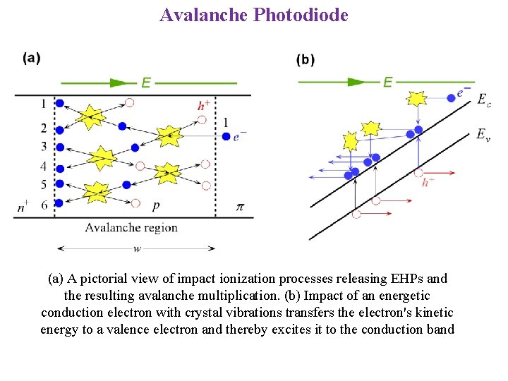
Avalanche Photodiode (a) A pictorial view of impact ionization processes releasing EHPs and the resulting avalanche multiplication. (b) Impact of an energetic conduction electron with crystal vibrations transfers the electron's kinetic energy to a valence electron and thereby excites it to the conduction band