Introduction to Verilog COE 202 Digital Logic Design

- Slides: 26

Introduction to Verilog COE 202 Digital Logic Design Dr. Muhamed Mudawar King Fahd University of Petroleum and Minerals

Presentation Outline v Hardware Description Language v Logic Simulation versus Synthesis v Verilog Module v Gate-Level Description and Gate Delays v Module Instantiation v Continuous Assignment v Writing a Simple Test Bench Introduction to Verilog COE 202 – Digital Logic Design © Muhamed Mudawar – slide 2

Hardware Description Language v Describes the hardware of digital systems in a textual form v Describes the hardware structures and behavior v Can represent logic diagrams, expressions, and complex circuits v NOT a software programming language v Two standard hardware description languages (HDLs) 1. Verilog (will be studied in this course) 2. VHDL (harder to learn than Verilog) Introduction to Verilog COE 202 – Digital Logic Design © Muhamed Mudawar – slide 3

Verilog = "Verifying Logic" v Invented as a simulation language in 1984 by Phil Moorby v Opened to public in 1990 by Cadence Design Systems v Became an IEEE standard in 1995 (Verilog-95) v Revised and upgraded in 2001 (Verilog-2001) v Revised also in 2005 (Verilog-2005) v Verilog allows designers to describe hardware at different levels ² Can describe anything from a single gate to a full computer system v Verilog is supported by the majority of electronic design tools v Verilog can be used for logic simulation and synthesis Introduction to Verilog COE 202 – Digital Logic Design © Muhamed Mudawar – slide 4

Logic Simulation v Logic simulator interprets the Verilog (HDL) description v Produces timing diagrams v Predicts how the hardware will behave before it is fabricated v Simulation allows the detection of functional errors in a design ² Without having to physically implement the circuit v Errors detected during the simulation can be corrected ² By modifying the appropriate statements in the Verilog description v Simulating and verifying a design requires a test bench v The test bench is also written in Verilog Introduction to Verilog COE 202 – Digital Logic Design © Muhamed Mudawar – slide 5

Logic Synthesis v Logic synthesis is similar to translating a program v However, the output of logic synthesis is a digital circuit v A digital circuit modeled in Verilog can be translated into a list of components and their interconnections, called netlist v Synthesis can be used to fabricate an integrated circuit v Synthesis can also target a Field Programmable Gate Array ² An FPGA chip can be configured to implement a digital circuit ² The digital circuit can also be modified by reconfiguring the FPGA v Logic simulation and synthesis are automated ² Using special software, called Electronic Design Automation (EDA) tools Introduction to Verilog COE 202 – Digital Logic Design © Muhamed Mudawar – slide 6

Verilog Module v A digital circuit is described in Verilog as a set of modules v A module is the design entity in Verilog v A module is declared using the module keyword v A module is terminated using the endmodule keyword v A module has a name and a list of input and output ports v A module is described by a group of statements v The statements can describe the module structure or behavior Introduction to Verilog COE 202 – Digital Logic Design © Muhamed Mudawar – slide 7

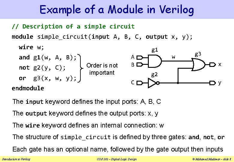
Example of a Module in Verilog // Description of a simple circuit module simple_circuit(input A, B, C, output x, y); wire w; g 1 and g 1(w, A, B); not g 2(y, C); or g 3(x, w, y); endmodule Order is not important A B w g 3 x g 2 C y The input keyword defines the input ports: A, B, C The output keyword defines the output ports: x, y The wire keyword defines an internal connection: w The structure of simple_circuit is defined by three gates: and, not, or Each gate has an optional name, followed by the gate output then inputs Introduction to Verilog COE 202 – Digital Logic Design © Muhamed Mudawar – slide 8

Verilog Syntax v Keywords: have special meaning in Verilog Many keywords: module, input, output, wire, and, or, etc. Keywords cannot be used as identifiers v Identifiers: are user-defined names for modules, ports, etc. Verilog is case-sensitive: A and a are different names v Comments: can be specified in two ways (similar to C) ² Single-line comments begin with // and terminate at end of line ² Multi-line comments are enclosed between /* and */ v White space: space, tab, newline can be used freely in Verilog v Operators: operate on variables (similar to C: ~ & | ^ + - etc. ) Introduction to Verilog COE 202 – Digital Logic Design © Muhamed Mudawar – slide 9

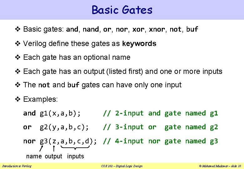
Basic Gates v Basic gates: and, nand, or, nor, xnor, not, buf v Verilog define these gates as keywords v Each gate has an optional name v Each gate has an output (listed first) and one or more inputs v The not and buf gates can have only one input v Examples: and g 1(x, a, b); // 2 -input and gate named g 1 or // 3 -input or g 2(y, a, b, c); gate named g 2 nor g 3(z, a, b, c, d); // 4 -input nor gate named g 3 name output inputs Introduction to Verilog COE 202 – Digital Logic Design © Muhamed Mudawar – slide 10

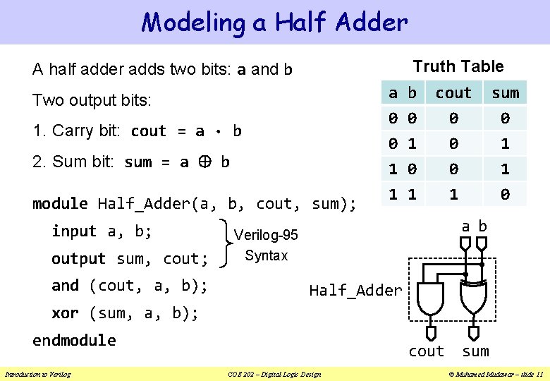
Modeling a Half Adder Truth Table A half adder adds two bits: a and b a 0 0 1 Two output bits: 1. Carry bit: cout = a · b 2. Sum bit: sum = a b module Half_Adder(a, b, cout, sum); input a, b; output sum, cout; and (cout, a, b); b 0 1 1 cout 0 0 0 sum 0 1 1 1 0 a b Verilog-95 Syntax Half_Adder xor (sum, a, b); endmodule Introduction to Verilog cout sum COE 202 – Digital Logic Design © Muhamed Mudawar – slide 11

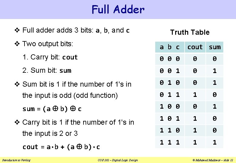
Full Adder v Full adder adds 3 bits: a, b, and c v Two output bits: Truth Table a b c cout sum 1. Carry bit: cout 0 0 0 2. Sum bit: sum 0 0 1 0 1 0 0 1 the input is odd (odd function) 0 1 1 1 0 sum = (a b) c 1 0 0 0 1 1 0 1 1 1 v Sum bit is 1 if the number of 1's in v Carry bit is 1 if the number of 1's in the input is 2 or 3 cout = a·b + (a b)·c Introduction to Verilog COE 202 – Digital Logic Design © Muhamed Mudawar – slide 12

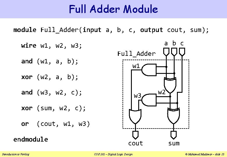
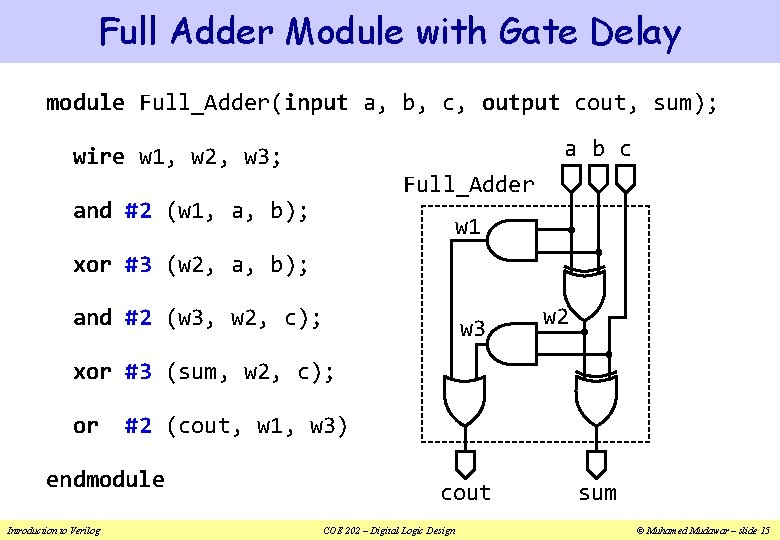
Full Adder Module module Full_Adder(input a, b, c, output cout, sum); wire w 1, w 2, w 3; and (w 1, a, b); a b c Full_Adder w 1 xor (w 2, a, b); and (w 3, w 2, c); w 3 w 2 xor (sum, w 2, c); or (cout, w 1, w 3) endmodule Introduction to Verilog cout COE 202 – Digital Logic Design sum © Muhamed Mudawar – slide 13

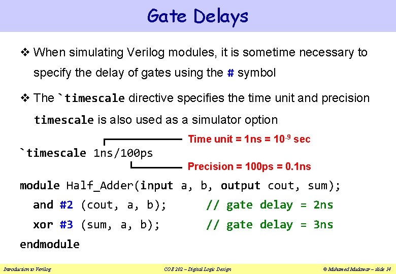
Gate Delays v When simulating Verilog modules, it is sometime necessary to specify the delay of gates using the # symbol v The `timescale directive specifies the time unit and precision timescale is also used as a simulator option Time unit = 1 ns = 10 -9 sec `timescale 1 ns/100 ps Precision = 100 ps = 0. 1 ns module Half_Adder(input a, b, output cout, sum); and #2 (cout, a, b); // gate delay = 2 ns xor #3 (sum, a, b); // gate delay = 3 ns endmodule Introduction to Verilog COE 202 – Digital Logic Design © Muhamed Mudawar – slide 14

Full Adder Module with Gate Delay module Full_Adder(input a, b, c, output cout, sum); a b c wire w 1, w 2, w 3; Full_Adder and #2 (w 1, a, b); w 1 xor #3 (w 2, a, b); and #2 (w 3, w 2, c); w 3 w 2 xor #3 (sum, w 2, c); or #2 (cout, w 1, w 3) endmodule Introduction to Verilog cout COE 202 – Digital Logic Design sum © Muhamed Mudawar – slide 15

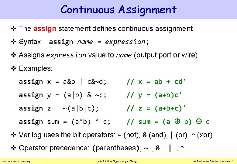
Continuous Assignment v The assign statement defines continuous assignment v Syntax: assign name = expression; v Assigns expression value to name (output port or wire) v Examples: assign x = a&b | c&~d; // x = ab + cd' assign y = (a|b) & ~c; // y = (a+b)c' assign z = ~(a|b|c); // z = (a+b+c)' assign sum = (a^b) ^ c; // sum = (a b) c v Verilog uses the bit operators: ~ (not), & (and), | (or), ^ (xor) v Operator precedence: (parentheses), ~ , & , | , ^ Introduction to Verilog COE 202 – Digital Logic Design © Muhamed Mudawar – slide 16

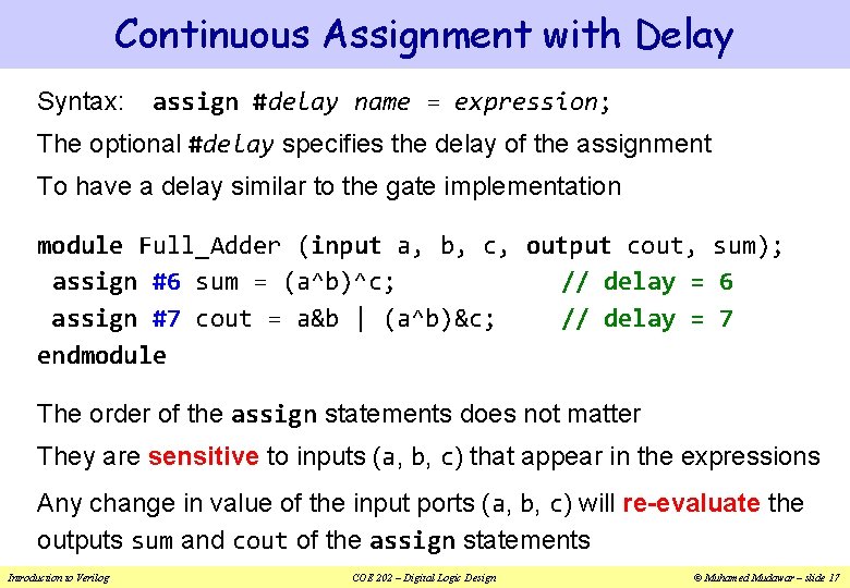
Continuous Assignment with Delay Syntax: assign #delay name = expression; The optional #delay specifies the delay of the assignment To have a delay similar to the gate implementation module Full_Adder (input a, b, c, output cout, sum); assign #6 sum = (a^b)^c; // delay = 6 assign #7 cout = a&b | (a^b)&c; // delay = 7 endmodule The order of the assign statements does not matter They are sensitive to inputs (a, b, c) that appear in the expressions Any change in value of the input ports (a, b, c) will re-evaluate the outputs sum and cout of the assign statements Introduction to Verilog COE 202 – Digital Logic Design © Muhamed Mudawar – slide 17

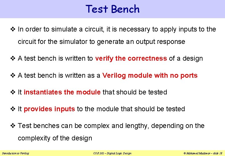
Test Bench v In order to simulate a circuit, it is necessary to apply inputs to the circuit for the simulator to generate an output response v A test bench is written to verify the correctness of a design v A test bench is written as a Verilog module with no ports v It instantiates the module that should be tested v It provides inputs to the module that should be tested v Test benches can be complex and lengthy, depending on the complexity of the design Introduction to Verilog COE 202 – Digital Logic Design © Muhamed Mudawar – slide 18

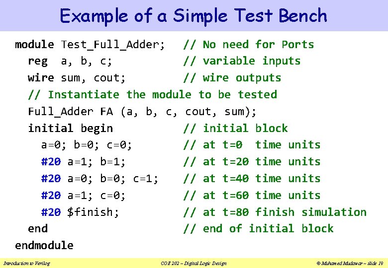
Example of a Simple Test Bench module Test_Full_Adder; // No need for Ports reg a, b, c; // variable inputs wire sum, cout; // wire outputs // Instantiate the module to be tested Full_Adder FA (a, b, c, cout, sum); initial begin // initial block a=0; b=0; c=0; // at t=0 time units #20 a=1; b=1; // at t=20 time units #20 a=0; b=0; c=1; // at t=40 time units #20 a=1; c=0; // at t=60 time units #20 $finish; // at t=80 finish simulation end // end of initial block endmodule Introduction to Verilog COE 202 – Digital Logic Design © Muhamed Mudawar – slide 19

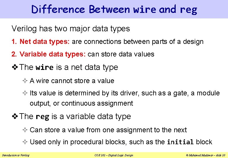
Difference Between wire and reg Verilog has two major data types 1. Net data types: are connections between parts of a design 2. Variable data types: can store data values v The wire is a net data type ² A wire cannot store a value ² Its value is determined by its driver, such as a gate, a module output, or continuous assignment v The reg is a variable data type ² Can store a value from one assignment to the next ² Used only in procedural blocks, such as the initial block Introduction to Verilog COE 202 – Digital Logic Design © Muhamed Mudawar – slide 20

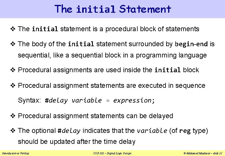
The initial Statement v The initial statement is a procedural block of statements v The body of the initial statement surrounded by begin-end is sequential, like a sequential block in a programming language v Procedural assignments are used inside the initial block v Procedural assignment statements are executed in sequence Syntax: #delay variable = expression; v Procedural assignment statements can be delayed v The optional #delay indicates that the variable (of reg type) should be updated after the time delay Introduction to Verilog COE 202 – Digital Logic Design © Muhamed Mudawar – slide 21

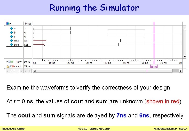
Running the Simulator Examine the waveforms to verify the correctness of your design At t = 0 ns, the values of cout and sum are unknown (shown in red) The cout and sum signals are delayed by 7 ns and 6 ns, respectively Introduction to Verilog COE 202 – Digital Logic Design © Muhamed Mudawar – slide 22

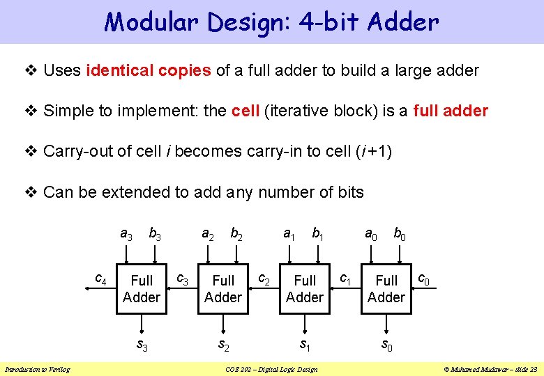
Modular Design: 4 -bit Adder v Uses identical copies of a full adder to build a large adder v Simple to implement: the cell (iterative block) is a full adder v Carry-out of cell i becomes carry-in to cell (i +1) v Can be extended to add any number of bits a 3 c 4 b 3 Full Adder s 3 Introduction to Verilog a 2 c 3 b 2 Full Adder s 2 a 1 c 2 b 1 Full Adder s 1 COE 202 – Digital Logic Design a 0 c 1 b 0 Full c 0 Adder s 0 © Muhamed Mudawar – slide 23

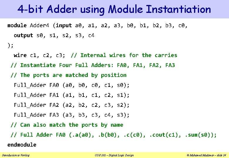
4 -bit Adder using Module Instantiation module Adder 4 (input a 0, a 1, a 2, a 3, b 0, b 1, b 2, b 3, c 0, output s 0, s 1, s 2, s 3, c 4 ); wire c 1, c 2, c 3; // Internal wires for the carries // Instantiate Four Full Adders: FA 0, FA 1, FA 2, FA 3 // The ports are matched by position Full_Adder FA 0 (a 0, b 0, c 1, s 0); Full_Adder FA 1 (a 1, b 1, c 2, s 1); Full_Adder FA 2 (a 2, b 2, c 3, s 2); Full_Adder FA 3 (a 3, b 3, c 4, s 3); // Can also match the ports by name // Full Adder FA 0 (. a(a 0), . b(b 0), . c(c 0), . cout(c 1), . sum(s 0)); endmodule Introduction to Verilog COE 202 – Digital Logic Design © Muhamed Mudawar – slide 24

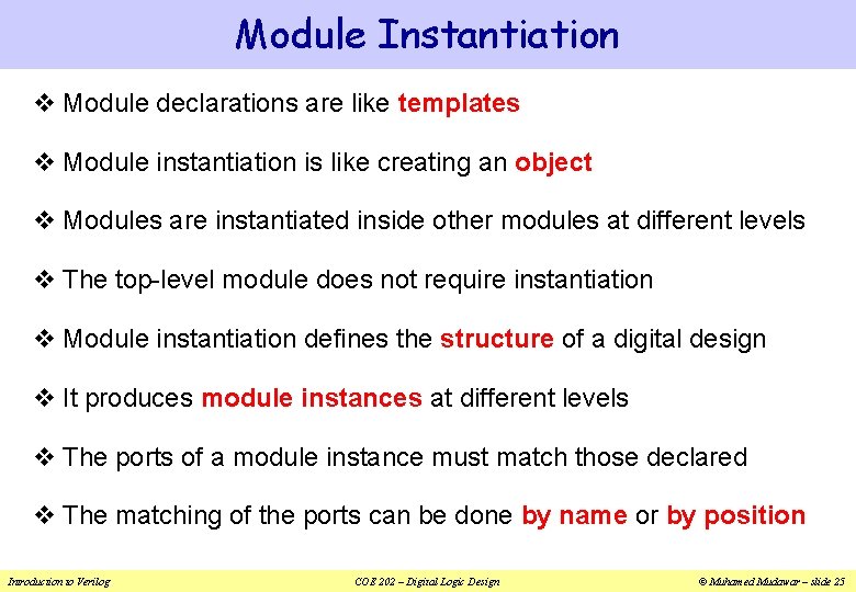
Module Instantiation v Module declarations are like templates v Module instantiation is like creating an object v Modules are instantiated inside other modules at different levels v The top-level module does not require instantiation v Module instantiation defines the structure of a digital design v It produces module instances at different levels v The ports of a module instance must match those declared v The matching of the ports can be done by name or by position Introduction to Verilog COE 202 – Digital Logic Design © Muhamed Mudawar – slide 25

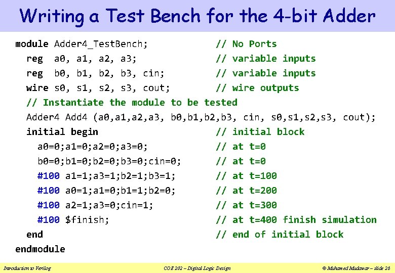
Writing a Test Bench for the 4 -bit Adder module Adder 4_Test. Bench; // No Ports reg a 0, a 1, a 2, a 3; // variable inputs reg b 0, b 1, b 2, b 3, cin; // variable inputs wire s 0, s 1, s 2, s 3, cout; // wire outputs // Instantiate the module to be tested Adder 4 Add 4 (a 0, a 1, a 2, a 3, b 0, b 1, b 2, b 3, cin, s 0, s 1, s 2, s 3, cout); initial begin // initial block a 0=0; a 1=0; a 2=0; a 3=0; // at t=0 b 0=0; b 1=0; b 2=0; b 3=0; cin=0; // at t=0 #100 a 1=1; a 3=1; b 2=1; b 3=1; // at t=100 #100 a 0=1; a 1=0; b 1=1; b 2=0; // at t=200 #100 a 2=1; a 3=0; cin=1; // at t=300 #100 $finish; // at t=400 finish simulation end // end of initial block endmodule Introduction to Verilog COE 202 – Digital Logic Design © Muhamed Mudawar – slide 26