COE 202 Digital Logic Design Courtesy of Dr

- Slides: 63

COE 202: Digital Logic Design Courtesy of Dr Radwan E Abdel-Aal Logic and Computer Design Fundamentals 11 Chapter 3 Unit – Combinational Logic Design Sequential Circuits Part 1 – Implementation Technology and Logic Design Charles Kime & Thomas Kaminski © 2004 Pearson Education, Inc. Terms of Use (Hyperlinks are active in View Show mode)

Unit 11: Sequential Circuits 1. Sequential Circuit Definitions, Types of Latches: SR, Clocked SR, and D Latches 2. Flip-Flops: SR, D, JK, and T Flip-Flops 3. Flip-Flop Timing Parameters: Setup, hold, propagation, clocking 4. Flip-Flops: Characteristic and Excitation Tables 5. Analysis of Sequential Circuits with D flip-flops: Deriving the input equations, state table, and state diagram. Timing. 6. Design of Sequential Circuits with D flip-flops: Determining the state diagrams and tables, State assignment, Combinational Logic Chapter 3 - Part 1 2

Logic and Computer Design Fundamentals Chapter 3 – Combinational Chapter 5 Logic - Sequential Design Circuits Part 1 – Implementation Technology and Logic Design Charles Kime & Thomas Kaminski © 2004 Pearson Education, Inc. Terms of Use (Hyperlinks are active in View Show mode)

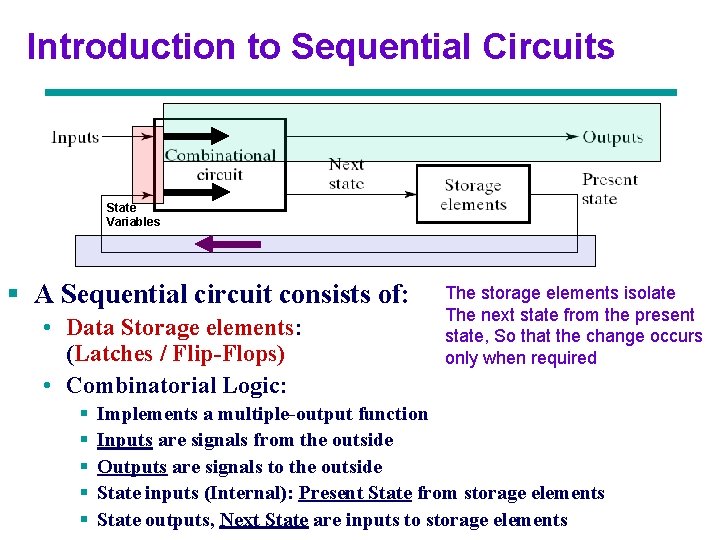
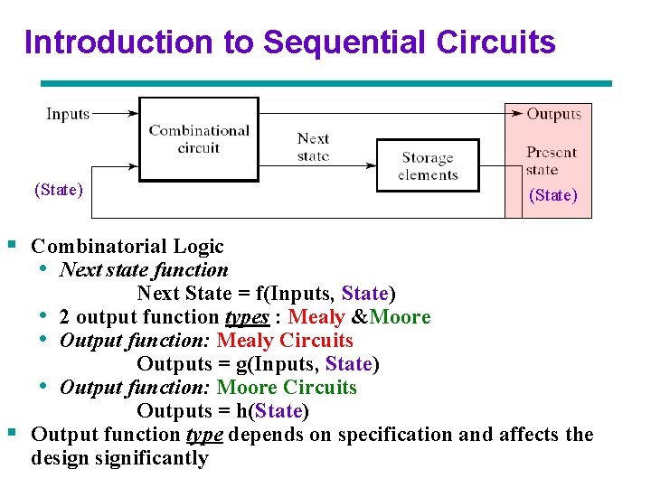
Introduction to Sequential Circuits State Variables § A Sequential circuit consists of: • Data Storage elements: (Latches / Flip-Flops) • Combinatorial Logic: § § § The storage elements isolate The next state from the present state, So that the change occurs only when required Implements a multiple-output function Inputs are signals from the outside Outputs are signals to the outside State inputs (Internal): Present State from storage elements State outputs, Next State are inputs to storage elements Chapter 3 - Part 1 4

Introduction to Sequential Circuits (State) § Combinatorial Logic • Next state function Next State = f(Inputs, State) • 2 output function types : Mealy &Moore • Output function: Mealy Circuits Outputs = g(Inputs, State) • Output function: Moore Circuits Outputs = h(State) § Output function type depends on specification and affects the designificantly Chapter 3 - Part 1 5

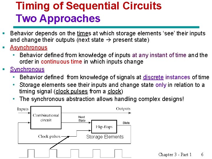
Timing of Sequential Circuits Two Approaches § Behavior depends on the times at which storage elements ‘see’ their inputs and change their outputs (next state present state) § Asynchronous • Behavior defined from knowledge of inputs at any instant of time and the order in continuous time in which inputs change § Synchronous • Behavior defined from knowledge of signals at discrete instances of time • Storage elements see their inputs and change state only in relation to a timing signal (clock pulses from a clock) • The synchronous abstraction allows handling complex designs! Storage Elements Chapter 3 - Part 1 6

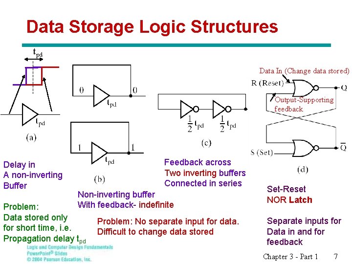
Data Storage Logic Structures tpd Data In (Change data stored) Output-Supporting feedback Delay in A non-inverting Buffer Feedback across Two inverting buffers Connected in series Non-inverting buffer With feedback- indefinite Problem: Data stored only for short time, i. e. Propagation delay tpd Problem: No separate input for data. Difficult to change data stored Set-Reset NOR Latch Separate inputs for Data in and for feedback Chapter 3 - Part 1 7

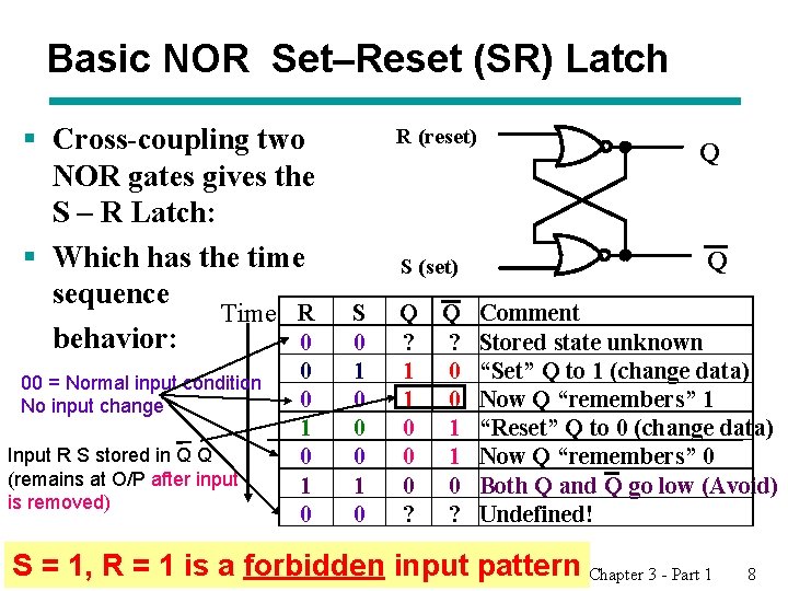
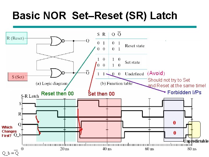
Basic NOR Set–Reset (SR) Latch § Cross-coupling two NOR gates gives the S – R Latch: § Which has the time sequence Time R behavior: 0 00 = Normal input condition No input change Input R S stored in Q Q (remains at O/P after input is removed) 0 0 1 0 R (reset) S (set) S 0 1 0 0 0 1 0 Q ? 1 1 0 0 0 ? Q ? 0 0 1 1 0 ? Q Q Comment Stored state unknown “Set” Q to 1 (change data) Now Q “remembers” 1 “Reset” Q to 0 (change data) Now Q “remembers” 0 Both Q and Q go low (Avoid) Undefined! S = 1, R = 1 is a forbidden input pattern Chapter 3 - Part 1 8

Basic NOR Set–Reset (SR) Latch Should not try to Set and Reset at the same time! Reset then 00 Which Changes First? Set then 00 Forbidden I/Ps 0 0 Unpredictable Q_b = Q Chapter 3 - Part 1 9

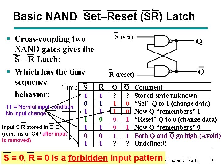
Basic NAND Set–Reset (SR) Latch § Cross-coupling two NAND gates gives the S – R Latch: § Which has the time sequence Time S behavior: 1 11 = Normal input condition No input change Input S R stored in Q Q (remains at O/P after input is removed) 0 1 1 1 0 1 R (reset) S (set) R 1 1 1 0 1 Q ? 1 1 0 0 1 ? Q ? 0 0 1 1 1 ? Q Q Comment Stored state unknown “Set” Q to 1 (change data) Now Q “remembers” 1 “Reset” Q to 0 (change data) Now Q “remembers” 0 Both Q and Q go high (Avoid) Undefined! S = 0, R = 0 is a forbidden input pattern Chapter 3 - Part 1 10

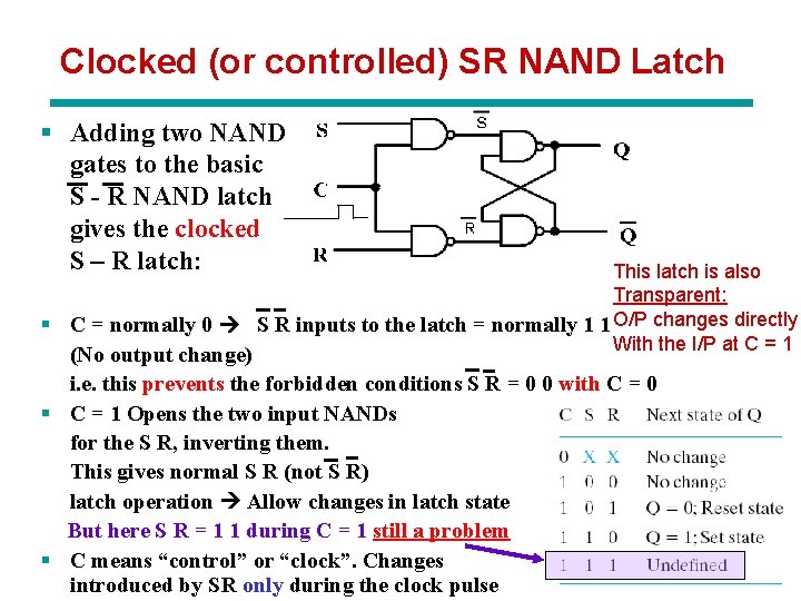
Clocked (or controlled) SR NAND Latch § Adding two NAND gates to the basic S - R NAND latch gives the clocked S – R latch: This latch is also Transparent: § C = normally 0 S R inputs to the latch = normally 1 1 O/P changes directly With the I/P at C = 1 (No output change) i. e. this prevents the forbidden conditions S R = 0 0 with C = 0 § C = 1 Opens the two input NANDs for the S R, inverting them. This gives normal S R (not S R) latch operation Allow changes in latch state But here S R = 1 1 during C = 1 still a problem § C means “control” or “clock”. Changes Chapter 3 - Part 1 introduced by SR only during the clock pulse 11

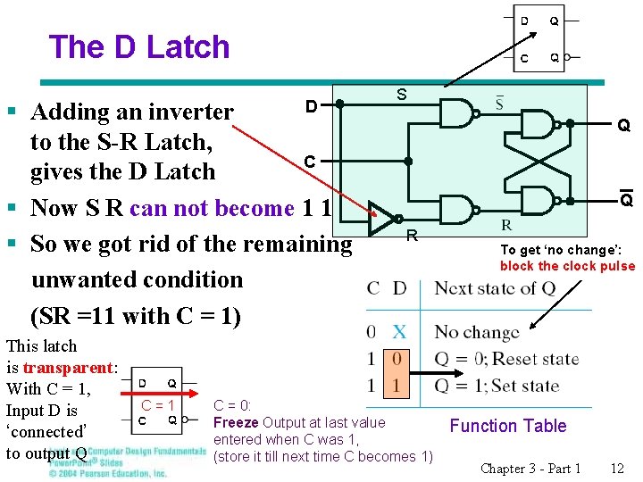
The D Latch D § Adding an inverter to the S-R Latch, C gives the D Latch § Now S R can not become 1 1 § So we got rid of the remaining unwanted condition (SR =11 with C = 1) This latch is transparent: With C = 1, Input D is ‘connected’ to output Q C = 1 S Q Q R C = 0: Freeze Output at last value entered when C was 1, (store it till next time C becomes 1) To get ‘no change’: block the clock pulse Function Table Chapter 3 - Part 1 12

Flip-Flops § The latch timing problem § Solution: Flip-Flop • Master-slave flip-flop • Edge-triggered flip-flop § Standard symbols for storage elements § Direct inputs to flip-flops § Flip-flop timing Chapter 3 - Part 1 13

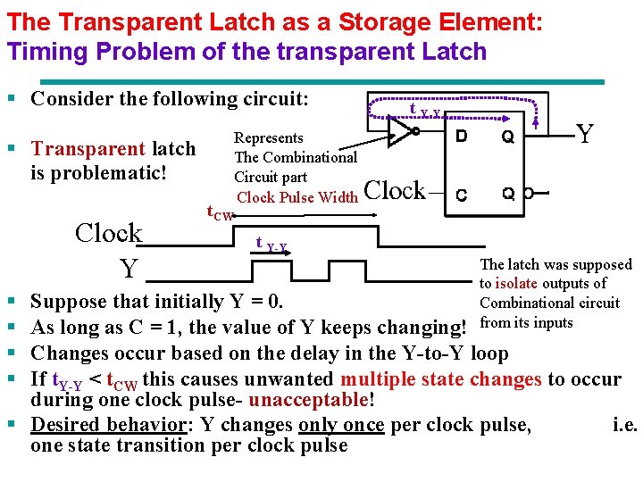
The Transparent Latch as a Storage Element: Timing Problem of the transparent Latch § Consider the following circuit: § Transparent latch is problematic! Clock Y § § t Y-Y Represents The Combinational Circuit part Clock Pulse Width t. CW t Y-Y The latch was supposed to isolate outputs of Combinational circuit from its inputs Suppose that initially Y = 0. As long as C = 1, the value of Y keeps changing! Changes occur based on the delay in the Y-to-Y loop If t. Y-Y < t. CW this causes unwanted multiple state changes to occur during one clock pulse- unacceptable! § Desired behavior: Y changes only once per clock pulse, i. e. one state transition per clock pulse Chapter 3 - Part 1 14

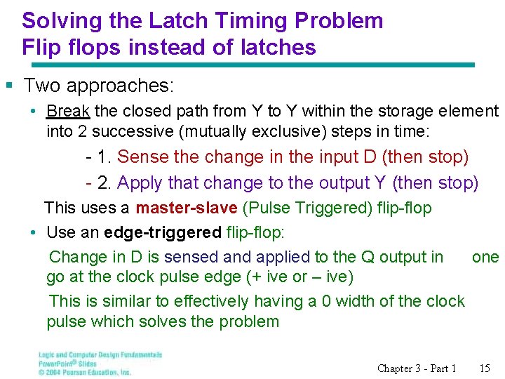
Solving the Latch Timing Problem Flip flops instead of latches § Two approaches: • Break the closed path from Y to Y within the storage element into 2 successive (mutually exclusive) steps in time: - 1. Sense the change in the input D (then stop) - 2. Apply that change to the output Y (then stop) This uses a master-slave (Pulse Triggered) flip-flop • Use an edge-triggered flip-flop: Change in D is sensed and applied to the Q output in one go at the clock pulse edge (+ ive or – ive) This is similar to effectively having a 0 width of the clock pulse which solves the problem Chapter 3 - Part 1 15

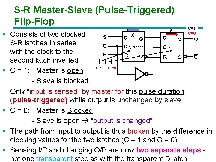
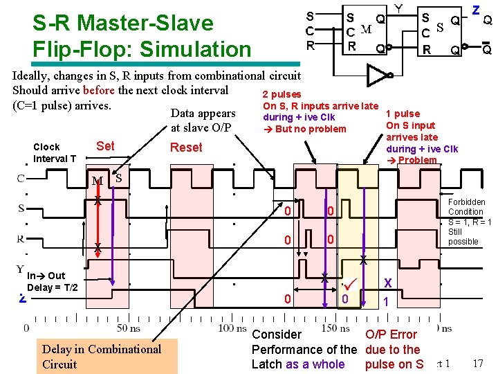
S-R Master-Slave (Pulse-Triggered) Flip-Flop X C=1 C=0 § Consists of two clocked S S X Q S Q Q S-R latches in series C C Master C Slave with the clock to the R R Q Q second latch inverted § C = 1: - Master is open C =1 C =0 - Slave is blocked Only “input is sensed” by master for this pulse duration (pulse-triggered) while output is unchanged by slave § C = 0: - Master is Blocked - Slave is open “output is changed” § The path from input to output is thus broken by the difference in clocking values for the two latches (C = 1 and C = 0) § Sensing I/P and changing O/P are now two separate steps - Chapter 3 - Part 1 16 not one transparent step as with the transparent D latch

Z S-R Master-Slave Flip-Flop: Simulation S Ideally, changes in S, R inputs from combinational circuit Should arrive before the next clock interval 2 pulses On S, R inputs arrive late (C=1 pulse) arrives. Data appears during + ive Clk at slave O/P But no problem Set Clock Reset Interval T 1 pulse On S input arrives late during + ive Clk Problem M S X X Z In Out Delay T/2 = T/2 Delay in Combinational Circuit 0 0 Forbidden Condition S = 1, R = 1 Still possible X X 0 0 X 1 Consider O/P Error Performance of the due to the Chapter 3 - Part 1 Latch as a whole pulse on S 17

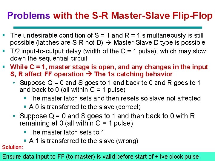
Problems with the S-R Master-Slave Flip-Flop § The undesirable condition of S = 1 and R = 1 simultaneously is still possible (latches are S-R not D) Master-Slave D type is possible § T/2 input-to-output delay (width of the C = 1 pulse), which may slow down the sequential circuit § While C = 1, master stage is open, and any changes in the input S, R affect FF operation The 1 s catching behavior • Suppose Q = 0 and S goes to 1 and back to 0 and R goes to 1 and back to 0 (all within C = 1 pulse) § The master latch sets and then resets so slave not affected § A 0 is transferred to the slave (correct) • Suppose Q = 0 and S goes to 1 and then back to 0 with R remaining at 0 (all within C = 1 pulse) § The master latch sets to 1 § A 1 is transferred to the slave (wrong) Solution: Chapter 3 - Part 1 Ensure data input to FF (to master) is valid before start of + ive clock pulse 18

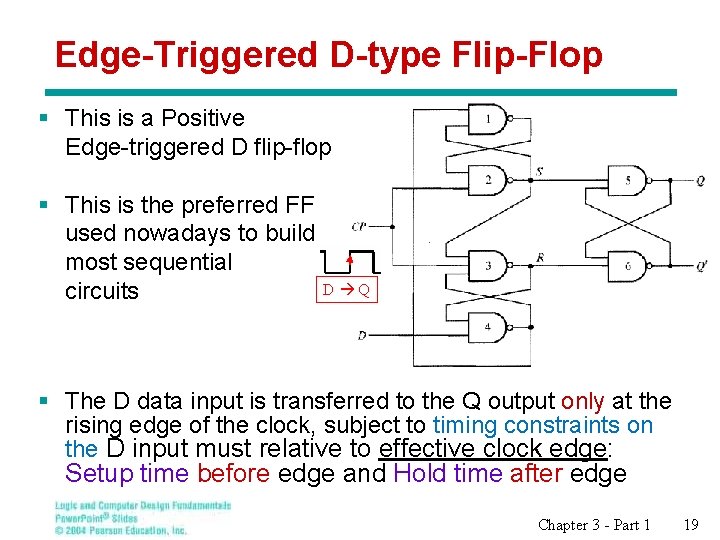
Edge-Triggered D-type Flip-Flop § This is a Positive Edge-triggered D flip-flop § This is the preferred FF used nowadays to build most sequential D Q circuits § The D data input is transferred to the Q output only at the rising edge of the clock, subject to timing constraints on the D input must relative to effective clock edge: Setup time before edge and Hold time after edge Chapter 3 - Part 1 19

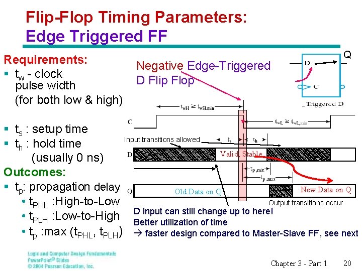
Flip-Flop Timing Parameters: Edge Triggered FF Requirements: § tw - clock pulse width (for both low & high) Negative Edge-Triggered D Flip Flop Q § ts : setup time Input transitions allowed § th : hold time Valid, Stable (usually 0 ns) Outcomes: § tp: propagation delay New Data on Q Old Data on Q • t. PHL : High-to-Low Output transitions occur • t. PLH : Low-to-High D input can still change up to here! Better utilization of time • tp : max (t. PHL, t. PLH) faster design compared to Master-Slave FF, see next Chapter 3 - Part 1 20

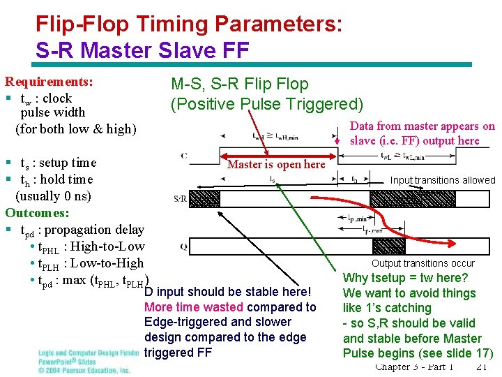
Flip-Flop Timing Parameters: S-R Master Slave FF Requirements: § tw : clock pulse width (for both low & high) M-S, S-R Flip Flop (Positive Pulse Triggered) Data from master appears on slave (i. e. FF) output here § ts : setup time § th : hold time (usually 0 ns) Outcomes: § tpd : propagation delay • t. PHL : High-to-Low • t. PLH : Low-to-High • tpd : max (t. PHL, t. PLH) Master is open here D input should be stable here! More time wasted compared to Edge-triggered and slower design compared to the edge triggered FF Input transitions allowed Output transitions occur Why tsetup = tw here? We want to avoid things like 1’s catching - so S, R should be valid and stable before Master Pulse begins (see slide 17) Chapter 3 - Part 1 21

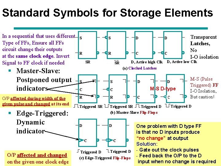
Standard Symbols for Storage Elements In a sequential that uses different Type of FFs, Ensure all FFs circuit change their outputs at the same clock edge. Invert Signal to FF clock if needed § Master-Slave: Postponed output indicators O/P affected during width of the given pulse and changed at its end § Edge-Triggered: Dynamic indicator S S D D R R C C SR D, Active low Clk (a) Clocked Latches S S C C R R Triggered SR Triggered D Triggered SR (b) Master-Slave Flip-Flops D D C O/P affected and changed on the given one clock edge D, Active high Clk SR Transparent Latches, No I-O isolation D D M-S D-type C C Triggered D (c) Edge-Triggered Flip-Flops C M-S (Pulse Triggered) FF I-O Isolation, But caution! Triggered D One problem with D type FF is that no D inputs produce “no change” at output Solution: - Gate out the clock pulses - Feed back the O/P to the D Chapter 3 - Part 1 22 input when no change is required

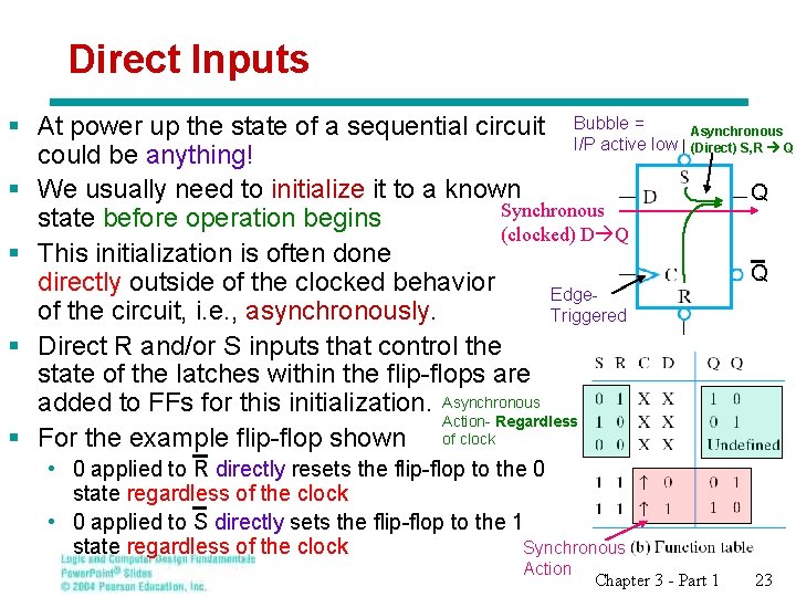
Direct Inputs § At power up the state of a sequential circuit Bubble = I/P active low could be anything! § We usually need to initialize it to a known Synchronous state before operation begins (clocked) D Q § This initialization is often done directly outside of the clocked behavior Edgeof the circuit, i. e. , asynchronously. Triggered § Direct R and/or S inputs that control the state of the latches within the flip-flops are added to FFs for this initialization. Asynchronous Action- Regardless § For the example flip-flop shown of clock Asynchronous (Direct) S, R Q Q Q • 0 applied to R directly resets the flip-flop to the 0 state regardless of the clock • 0 applied to S directly sets the flip-flop to the 1 Synchronous state regardless of the clock Action Chapter 3 - Part 1 23

Other Types of Flip-Flops § We know about the master-slave S-R and D flip-flops § We will briefly introduce J-K and T flip-flops • Implementation • Behavior Chapter 3 - Part 1 24

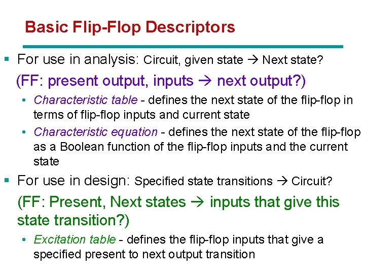
Basic Flip-Flop Descriptors § For use in analysis: Circuit, given state Next state? (FF: present output, inputs next output? ) • Characteristic table - defines the next state of the flip-flop in terms of flip-flop inputs and current state • Characteristic equation - defines the next state of the flip-flop as a Boolean function of the flip-flop inputs and the current state § For use in design: Specified state transitions Circuit? (FF: Present, Next states inputs that give this state transition? ) • Excitation table - defines the flip-flop inputs that give a specified present to next output transition Chapter 3 - Part 1 25

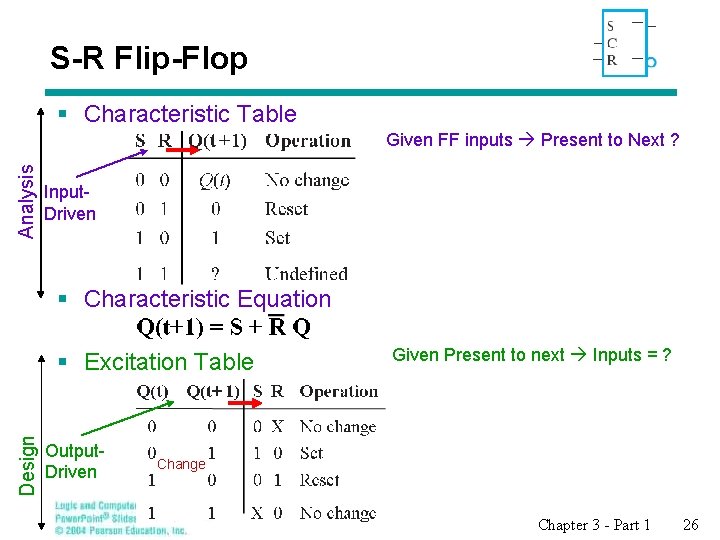
S-R Flip-Flop § Characteristic Table Analysis Given FF inputs Present to Next ? Input. Driven § Characteristic Equation Design § Excitation Table Output. Driven Given Present to next Inputs = ? Change Chapter 3 - Part 1 26

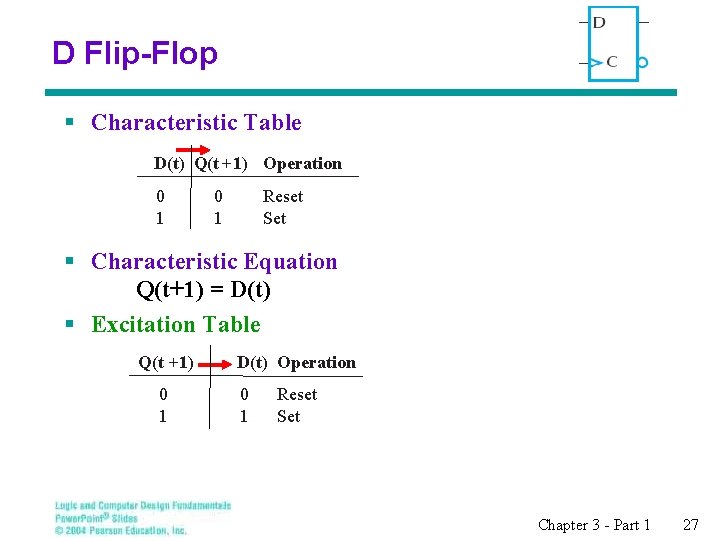
D Flip-Flop § Characteristic Table D(t) Q(t + 1) Operation 0 1 Reset Set § Characteristic Equation Q(t+1) = D(t) § Excitation Table Q(t +1) 0 1 D(t) Operation 0 1 Reset Set Chapter 3 - Part 1 27

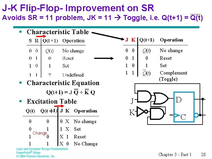
J-K Flip-Flop- Improvement on SR Avoids SR = 11 problem, JK = 11 Toggle, i. e. Q(t+1) = Q(t) § Characteristic Table J K Q(t+1) Operation 0 0 1 1 No change Reset Set Complement (Toggle) 0 1 § Characteristic Equation § Excitation Table Q(t) Q(t +1) J K Operation 0 0 0 1 Change 1 0 1 X X 1 0 No change Set Reset No Change J K Q(t) 0 1 Q(t) D C Chapter 3 - Part 1 28

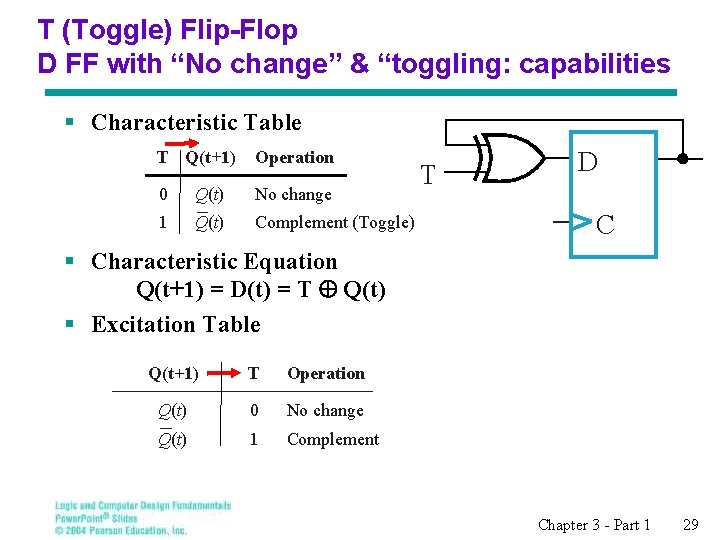
T (Toggle) Flip-Flop D FF with “No change” & “toggling: capabilities § Characteristic Table T Q(t +1) Operation 0 Q(t) No change 1 Q(t) Complement (Toggle) T D C § Characteristic Equation Q(t+1) = D(t) = T Å Q(t) § Excitation Table Q(t +1) T Operation Q(t) 0 No change Q(t) 1 Complement Chapter 3 - Part 1 29

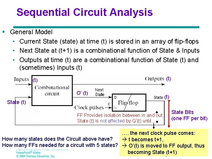
Sequential Circuit Analysis § General Model • Current State (state) at time (t) is stored in an array of flip-flops • Next State at (t+1) is a combinational function of State & Inputs • Outputs at time (t) are a combinational function of State (t) and (sometimes) Inputs (t) (t) O’ (t) State (t) FF Provides isolation between in and out: State (t) is not affected by Q’(t) until…. . State Bits (one FF per bit) …. the next clock pulse comes: How many states does the Circuit above have? t becomes t+1, How many FFs needed for a circuit with 5 states? O’(t) is moved to FF output, thus becoming State (t+1) Chapter 3 - Part 1 30

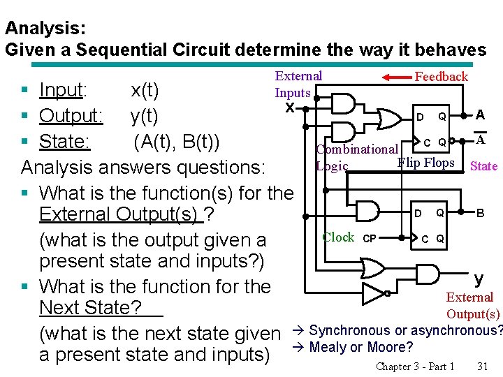
Analysis: Given a Sequential Circuit determine the way it behaves External Inputs Feedback § Input: x(t) x A D Q § Output: y(t) A C Q § State: (A(t), B(t)) Combinational Flip Flops State Logic Analysis answers questions: § What is the function(s) for the B D Q External Output(s) ? Clock CP C Q (what is the output given a present state and inputs? ) y § What is the function for the External Next State? Output(s) (what is the next state given Synchronous or asynchronous? a present state and inputs) Mealy or Moore? Chapter 3 - Part 1 31

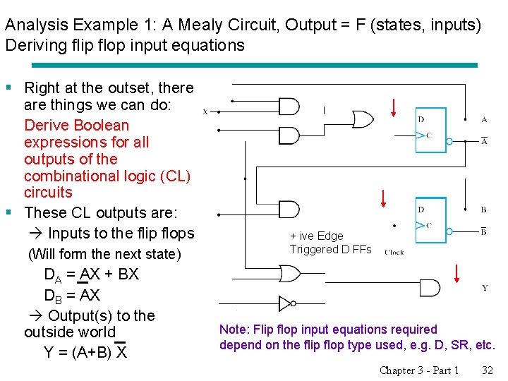
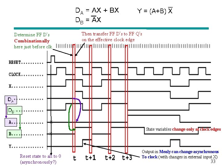
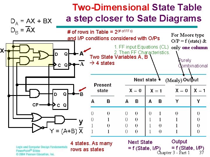
Analysis Example 1: A Mealy Circuit, Output = F (states, inputs) Deriving flip flop input equations § Right at the outset, there are things we can do: Derive Boolean expressions for all outputs of the combinational logic (CL) circuits § These CL outputs are: Inputs to the flip flops (Will form the next state) DA = AX + BX DB = AX Output(s) to the outside world Y = (A+B) X + ive Edge Triggered D FFs Note: Flip flop input equations required depend on the flip flop type used, e. g. D, SR, etc. Chapter 3 - Part 1 32

Then transfer FF D’s to FF Q’s on the effective clock edge Determine FF D’s Combinationally here just before clk 1 0 X X Reset state to all to 0 (asynchronously? ) 1 0 0 0 1 State variables change only at clock edges 0 Output in Mealy can change asynchronous To clock (with changes in external input X) Chapter 3 - Part 1 33

Sequential Circuit Analysis § Given a sequential Circuit § Objective: Derive outputs & state behavior (outputs and next state) from (present states and inputs) § Two equivalent approaches to represent the results: • State table: A truth table-like approach • State diagram: A graphical, more intuitive way of representing the state table and expressing the sequential circuit operation Chapter 3 - Part 1 34

State Table Characteristics § State table – a multiple variable table with the following four sections: CL Inputs: • Present State – the values of the state variables for each allowed state (FF outputs) • External Inputs CL Outputs: • Next-state – the value of the state (FF outputs) at time (t+1) based on the present state and the inputs. Determined by FF inputs & FF characteristics • Outputs – the value of the outputs as a function of the present state and (sometimes- Mealy) the inputs. Chapter 3 - Part 1 35

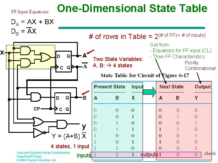
FF Input Equations: One-Dimensional State Table # of rows in Table = 2(# of FFs+ # of inputs) x Q A C Q A Q B D D CP Two State Variables: A, B: 4 states Get from: - Equations for FF input (CL) - Then FF Characteristics. Purely Combinational C Q y 4 states, 1 inputs outputs Chapter 3 - Part 1 check 36

Two-Dimensional State Table a step closer to Sate Diagrams # of rows in Table = 2(# of FFs) and I/P conditions considered with O/Ps For Moore type O/P = f (state) & 1. FF input Equations (CL) only one column x Q A C Q A D 2. Then FF Characteristics. Two State Variables A, B 4 states Purely Combinational (Mealy) D CP Q B C Q y 4 states. As many rows as states Next State = f (State, I/P) Output = f (State, I/P) Chapter 3 - Part 1 37

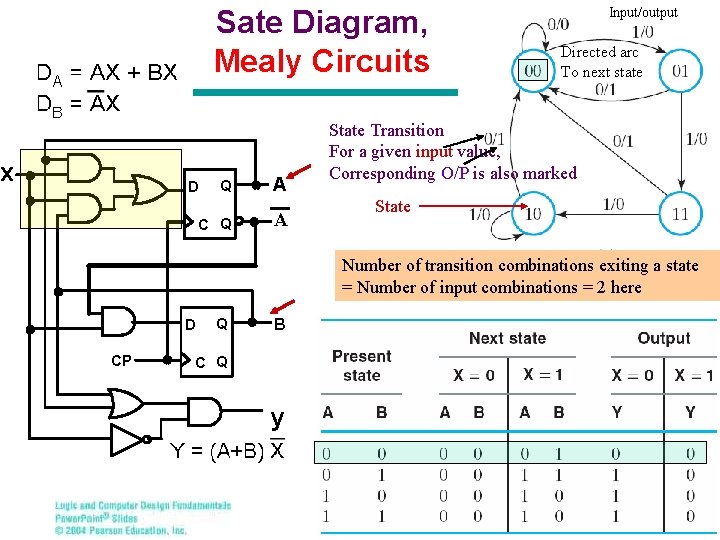
Sate Diagram, Mealy Circuits x D Q C Q A A Input/output Directed arc To next state State Transition For a given input value, Corresponding O/P is also marked State Number of transition combinations exiting a state = Number of input combinations = 2 here D CP Q B C Q y Chapter 3 - Part 1 38

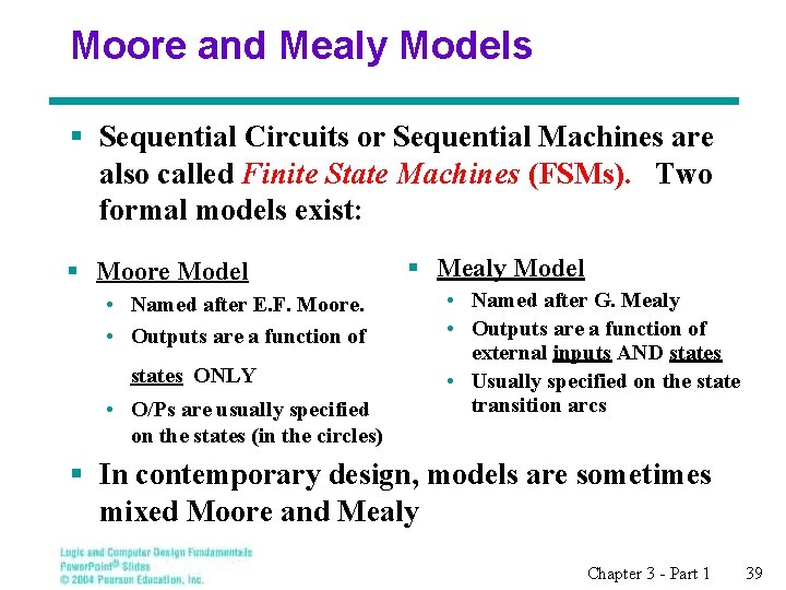
Moore and Mealy Models § Sequential Circuits or Sequential Machines are also called Finite State Machines (FSMs). Two formal models exist: § Moore Model • Named after E. F. Moore. • Outputs are a function of states ONLY • O/Ps are usually specified on the states (in the circles) § Mealy Model • Named after G. Mealy • Outputs are a function of external inputs AND states • Usually specified on the state transition arcs § In contemporary design, models are sometimes mixed Moore and Mealy Chapter 3 - Part 1 39

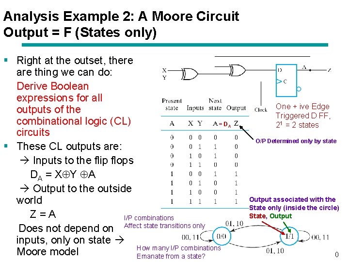
Analysis Example 2: A Moore Circuit Output = F (States only) § Right at the outset, there are thing we can do: Derive Boolean expressions for all outputs of the combinational logic (CL) =D circuits § These CL outputs are: Inputs to the flip flops DA = X Y A Output to the outside world Z = A I/P combinations Does not depend on Affect state transitions only inputs, only on state How many I/P combinations Moore model Emanate from a state? A One + ive Edge Triggered D FF, 21 = 2 states O/P Determined only by state Output associated with the State only (inside the circle) State, Output Chapter 3 - Part 1 40

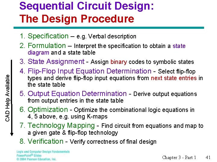
Sequential Circuit Design: The Design Procedure 1. Specification – e. g. Verbal description 2. Formulation – Interpret the specification to obtain a state CAD Help Available diagram and a state table 3. State Assignment - Assign binary codes to symbolic states 4. Flip-Flop Input Equation Determination - Select flip-flop types and derive flip-flop input equations from next state entries in the state table 5. Output Equation Determination - Derive output equations from output entries in the state table 6. Optimization - Optimize the combinational logic equations in 4, 5 above, e. g. using K-maps 7. Technology Mapping - Find circuit from equations and map to a given gate & flip-flop technology 8. Verification - Verify correctness of final design Chapter 3 - Part 1 41

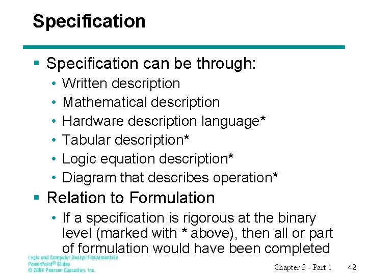
Specification § Specification can be through: • • • Written description Mathematical description Hardware description language* Tabular description* Logic equation description* Diagram that describes operation* § Relation to Formulation • If a specification is rigorous at the binary level (marked with * above), then all or part of formulation would have been completed Chapter 3 - Part 1 42

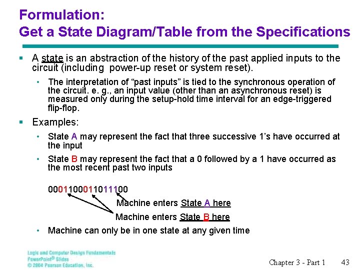
Formulation: Get a State Diagram/Table from the Specifications § A state is an abstraction of the history of the past applied inputs to the circuit (including power-up reset or system reset). • The interpretation of “past inputs” is tied to the synchronous operation of the circuit. e. g. , an input value (other than an asynchronous reset) is measured only during the setup-hold time interval for an edge-triggered flip-flop. § Examples: • State A may represent the fact that three successive 1’s have occurred at the input • State B may represent the fact that a 0 followed by a 1 have occurred as the most recent past two inputs 00011011100 Machine enters State A here Machine enters State B here • Machine can only be in one state at any given time Chapter 3 - Part 1 43

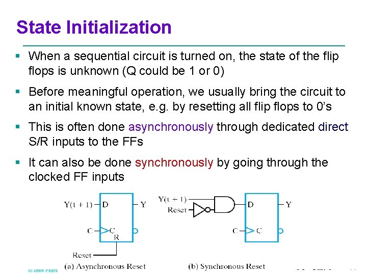
State Initialization § When a sequential circuit is turned on, the state of the flip flops is unknown (Q could be 1 or 0) § Before meaningful operation, we usually bring the circuit to an initial known state, e. g. by resetting all flip flops to 0’s § This is often done asynchronously through dedicated direct S/R inputs to the FFs § It can also be done synchronously by going through the clocked FF inputs Chapter 3 - Part 1 44

Example: Bit Sequence Recognizer: 1101 1. Specifications- Verbal Specifications: X Input Z 1101 Recognizer Output § Detect the occurrence of bit sequence 1101 whenever it occurs on input X and indicate this detection by raising an output Z high § i. e. normally output Z = 0 until sequence 1101 occurs i. e. until input X = 1 and 110 was the last sub-sequence received i. e. system was in the state ‘ 110 received’ § Is this a Mealy or a Moore model? Chapter 3 - Part 1 45

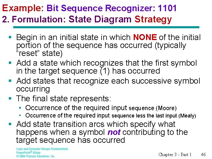
Example: Bit Sequence Recognizer: 1101 2. Formulation: State Diagram Strategy § Begin in an initial state in which NONE of the initial portion of the sequence has occurred (typically “reset” state) § Add a state which recognizes that the first symbol in the target sequence (1) has occurred § Add states that recognize each successive symbol occurring § The final state represents: • Occurrence of the required input sequence (Moore) • Occurrence of the required input sequence less the last input (Mealy) § Add state transition arcs which specify what happens when a symbol not contributing to the target sequence has occurred Chapter 3 - Part 1 46

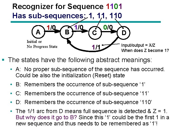
Recognizer for Sequence 1101 Has sub-sequences: 1, 110 A 1/0 Initial or No Progress State B 1/0 C 1/1 0/0 D Input/output = X/Z When does Z become 1? § The states have the following abstract meanings: • A: No proper sub-sequence of the sequence has occurred. Could be also the initialization (Reset) state • B: Remembers the occurrence of sub-sequence ‘ 1’ • C: Remembers the occurrence of sub-sequence ‘ 11’ • D: Remembers the occurrence of sub-sequence ‘ 110’ • The 1/1 arc from D means full sequence is detected & Z = 1. But why does it go to B? Since this ‘ 1’ could be the first 1 in a new sequence and thus needs to be remembered as ‘ 1’! Chapter 3 - Part 1 47

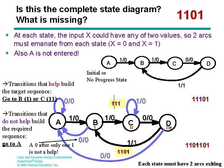
Is this the complete state diagram? What is missing? 1101 § At each state, the input X could have any of two values, so 2 arcs must emanate from each state (X = 0 and X = 1) § Also A is not entered! 1/0 A Transitions that help build the target sequence: Go to B (1) or C (11) 0/0 11101 1/0 C 11 1/1 0/0 D 1/1 111 1/0 0/0 C Initial or No Progress State Transitions that 1/0 do not help build A B 1 the required sequence: 0/0 go to A A 0 after only one 1 is not a help! B 1101 0/0 D 1101101 Chapter 3 - 2 Part 1 exiting 48 Each state must have arcs

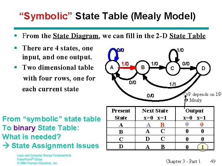
“Symbolic” State Table (Mealy Model) § From the State Diagram, we can fill in the 2 -D State Table § There are 4 states, one input, and one output. § Two dimensional table with four rows, one for each current state 0/0 A 1/0 1/0 B C 0/0 From “symbolic” state table To binary State Table: What is needed? State Assignment Issues D 1/1 O/P depends on I/P, Mealy 0/0 Present State A B C D 0/0 Next State x=0 x=1 A A D A B C C B Output x=0 x=1 0 0 0 0 1 Chapter 3 - Part 1 49

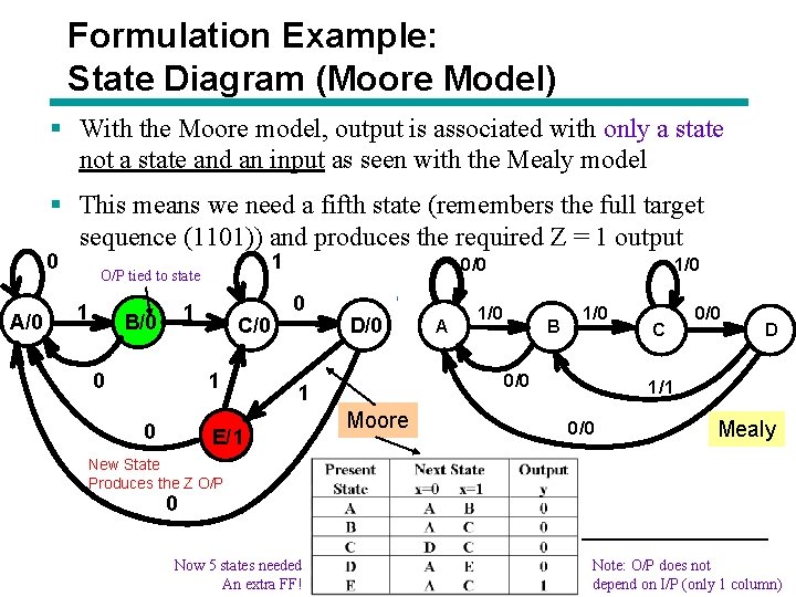
Formulation Example: State Diagram (Moore Model) § With the Moore model, output is associated with only a state not a state and an input as seen with the Mealy model § This means we need a fifth state (remembers the full target sequence (1101)) and produces the required Z = 1 output 0 A/0 1 O/P tied to state 1 1 B/0 0 C/0 1 0 0/0 0 D/0 1/0 B 1/0 0/0 1 E/1 A 1/0 Moore C 0/0 D 1/1 0/0 Mealy New State Produces the Z O/P 0 Now 5 states needed An extra FF! Note: O/P does not Chapter - Part 50 depend on 3 I/P (only 11 column)

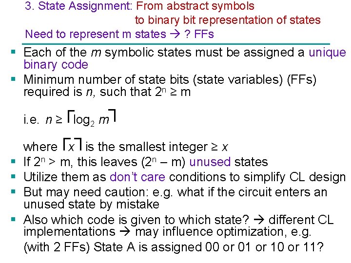
3. State Assignment: From abstract symbols to binary bit representation of states Need to represent m states ? FFs § Each of the m symbolic states must be assigned a unique binary code § Minimum number of state bits (state variables) (FFs) required is n, such that 2 n ≥ m i. e. n ≥ log 2 m § § where x is the smallest integer ≥ x If 2 n > m, this leaves (2 n – m) unused states Utilize them as don’t care conditions to simplify CL design But may need caution: e. g. what if the circuit enters an unused state by mistake Also which code is given to which state? different CL implementations may influence optimization, e. g. (with 2 FFs) State A is assigned 00 or 01 or 10 or 11? Chapter 3 - Part 1 51

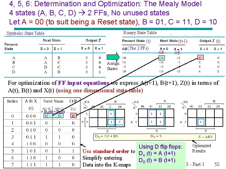
4, 5, 6: Determination and Optimization: The Mealy Model 4 states (A, B, C, D) 2 FFs, No unused states Let A = 00 (to suit being a Reset state), B = 01, C = 11, D = 10 Binary State Table Symbolic State Table (t) (The 2 FFs) (t+1) AB (t) AB Assign States For optimization of FF input equations we express A(t+1), B(t+1), Z(t) in terms of A(t), B(t) and X(t) (using one dimensional state table) = DA(t) = DB(t) Optimized Using D flip flops: Results Use standard order to D (t) = A (t+1) A Simplify entering DB (t) = B (t+1) Chapter 3 - Part 1 52 Data into the K-maps

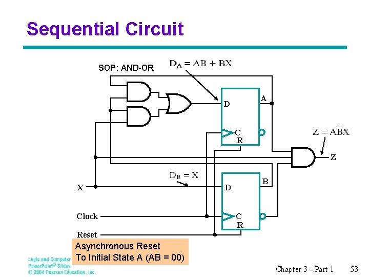
Sequential Circuit SOP: AND-OR A D C R Z X Clock B D C R Reset Asynchronous Reset To Initial State A (AB = 00) Chapter 3 - Part 1 53

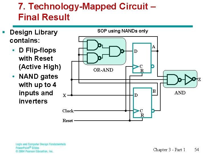
7. Technology-Mapped Circuit – Final Result § Design Library contains: • D Flip-flops with Reset (Active High) • NAND gates with up to 4 inputs and X inverters Clock SOP using NANDs only A D C R OR-AND Z B D AND C R Reset Chapter 3 - Part 1 54

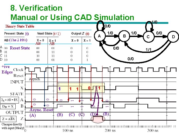
8. Verification Manual or Using CAD Simulation 1/0 0/0 A A B C D 1/0 Reset State B 1/0 0/0 C 0/0 D 1/1 0/0 +ive Edges Asynch. 1 Changes directly with input (Mealy) 0 1 (C) (D) (B) 0 1 1 1 0 1 Async. Reset (B) (A) 0 1 1 1 0 0 1 Chapter 3 - Part 1 55

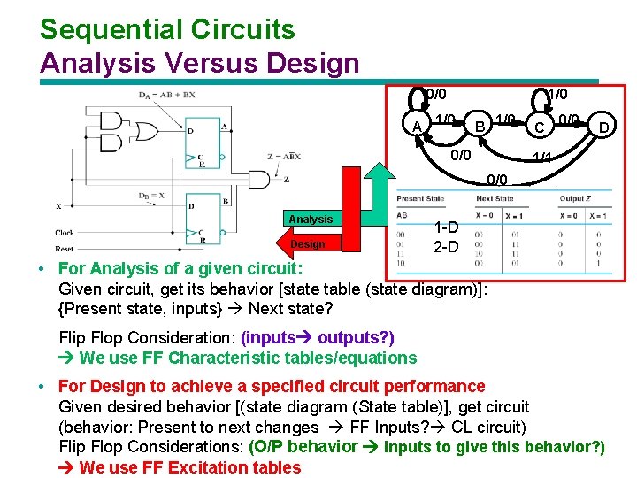
Sequential Circuits Analysis Versus Design 0/0 1/0 A 1/0 B 1/0 0/0 C 0/0 D 1/1 0/0 Analysis Design 1 -D 2 -D • For Analysis of a given circuit: Given circuit, get its behavior [state table (state diagram)]: {Present state, inputs} Next state? Flip Flop Consideration: (inputs outputs? ) We use FF Characteristic tables/equations • For Design to achieve a specified circuit performance Given desired behavior [(state diagram (State table)], get circuit (behavior: Present to next changes FF Inputs? CL circuit) Flip Flop Considerations: (O/P behavior inputs to give this behavior? ) Chapter 3 - Part 1 56 We use FF Excitation tables

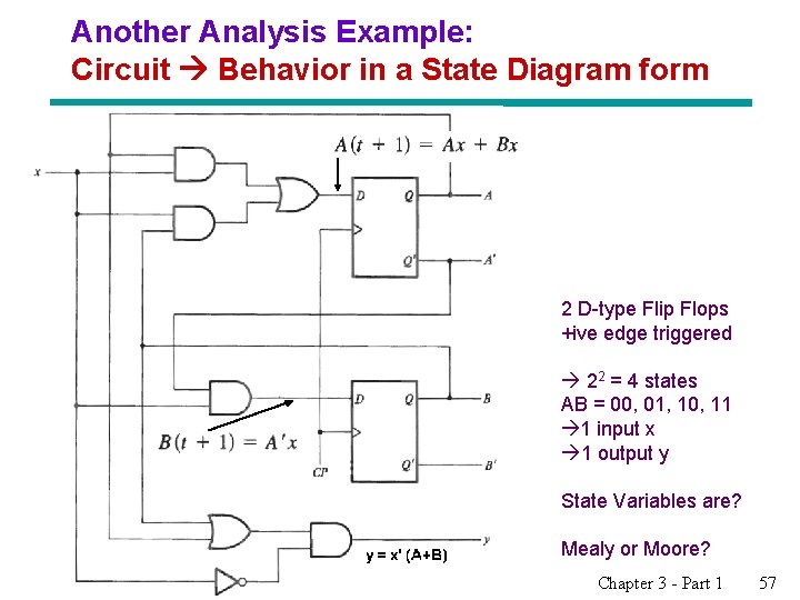
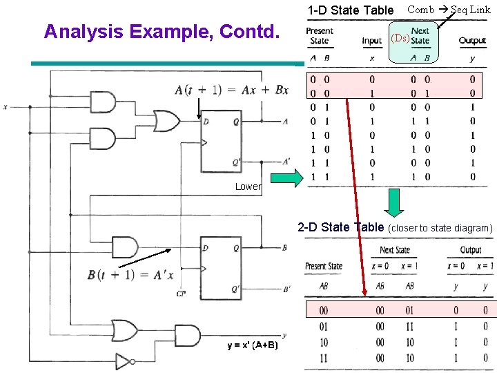
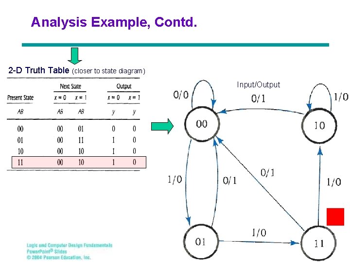
Another Analysis Example: Circuit Behavior in a State Diagram form 2 D-type Flip Flops +ive edge triggered 22 = 4 states AB = 00, 01, 10, 11 1 input x 1 output y State Variables are? Mealy or Moore? Chapter 3 - Part 1 57

1 -D State Table Analysis Example, Contd. Comb Seq Link (Ds) Lower 2 -D State Table (closer to state diagram) Chapter 3 - Part 1 58

Analysis Example, Contd. 2 -D Truth Table (closer to state diagram) Input/Output Chapter 3 - Part 1 59

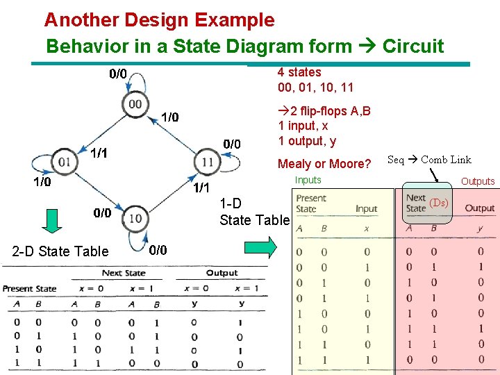
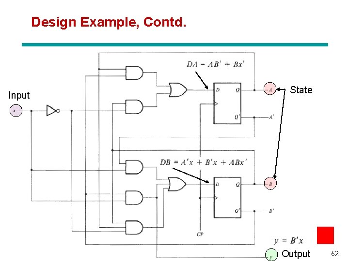
Another Design Example Behavior in a State Diagram form Circuit 4 states 00, 01, 10, 11 2 flip-flops A, B 1 input, x 1 output, y Mealy or Moore? Seq Comb Link Inputs 1 -D State Table Outputs (Ds) 2 -D State Table Chapter 3 - Part 1 60

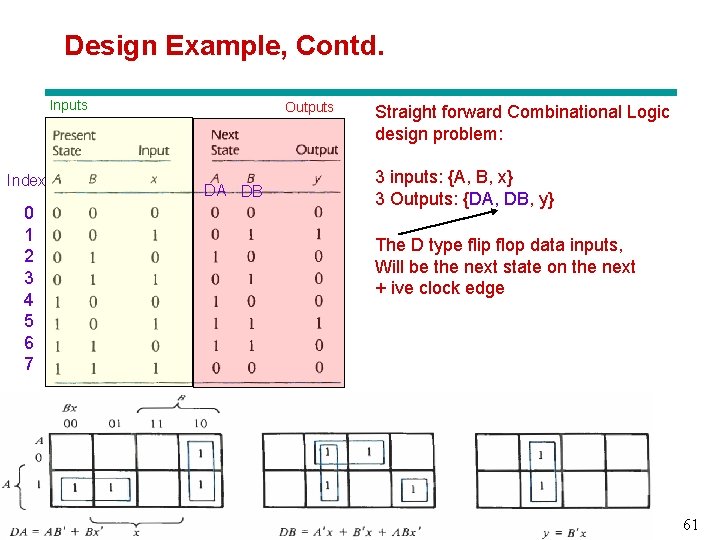
Design Example, Contd. Inputs Index 0 1 2 3 4 5 6 7 Outputs DA DB Straight forward Combinational Logic design problem: 3 inputs: {A, B, x} 3 Outputs: {DA, DB, y} The D type flip flop data inputs, Will be the next state on the next + ive clock edge Chapter 3 - Part 1 61

Design Example, Contd. Input State Chapter. Output 3 - Part 1 62

Unit 11: Sequential Circuits Chapters 5 & 6: Sequential Circuits 1. Sequential Circuit Definitions, Types of Latches: SR, Clocked SR, and D Latches 2. Flip-Flops: SR, D, JK, and T Flip-Flops 3. Flip-Flop Timing Parameters: Setup, hold, propagation, clocking 4. Flip-Flops: Characteristic and Excitation Tables 5. Analysis of Sequential Circuits with D flip-flops: Deriving the input equations, state table, and state diagram. Timing 6. Design of Sequential Circuits with D flip-flops: Determining the state diagrams and tables, State assignment, Combinational Logic Chapter 3 - Part 1 63