Modeling Sequential Circuits in Verilog COE 202 Digital

![Test Bench for the Up-Down Counter module Up_Down_Counter_TB; // Test Bench reg [7: 0] Test Bench for the Up-Down Counter module Up_Down_Counter_TB; // Test Bench reg [7: 0]](https://slidetodoc.com/presentation_image_h/37d77b92db5d42e82226c4759ad03e8b/image-26.jpg)
- Slides: 27

Modeling Sequential Circuits in Verilog COE 202 Digital Logic Design Dr. Muhamed Mudawar King Fahd University of Petroleum and Minerals

Presentation Outline v Blocking versus Non-Blocking Assignments v Modeling Latches and Flip-Flops v Modeling Sequential Circuit Diagrams v Modeling Mealy and Moore State Diagrams v Writing Test Benches for Sequential Circuits v Modeling Registers and Counters Modeling Sequential Circuits in Verilog COE 202 – Digital Logic Design © Muhamed Mudawar – slide 2

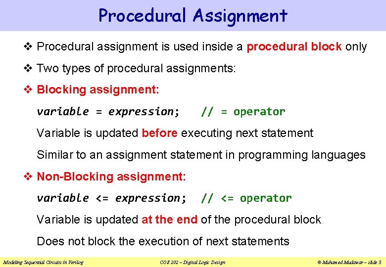
Procedural Assignment v Procedural assignment is used inside a procedural block only v Two types of procedural assignments: v Blocking assignment: variable = expression; // = operator Variable is updated before executing next statement Similar to an assignment statement in programming languages v Non-Blocking assignment: variable <= expression; // <= operator Variable is updated at the end of the procedural block Does not block the execution of next statements Modeling Sequential Circuits in Verilog COE 202 – Digital Logic Design © Muhamed Mudawar – slide 3

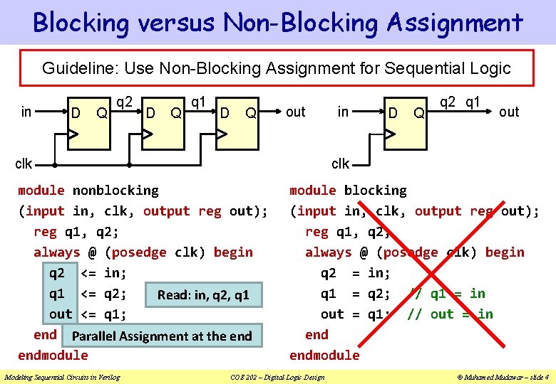
Blocking versus Non-Blocking Assignment Guideline: Use Non-Blocking Assignment for Sequential Logic in D Q q 2 D Q q 1 D Q out clk module nonblocking (input in, clk, output reg out); reg q 1, q 2; always @ (posedge clk) begin q 2 <= in; q 1 <= q 2; Read: in, q 2, q 1 out <= q 1; end Parallel Assignment at the endmodule Modeling Sequential Circuits in Verilog in q 2 q 1 module blocking (input in, clk, output reg out); reg q 1, q 2; always @ (posedge clk) begin q 2 = in; q 1 = q 2; // q 1 = in out = q 1; // out = in endmodule COE 202 – Digital Logic Design © Muhamed Mudawar – slide 4

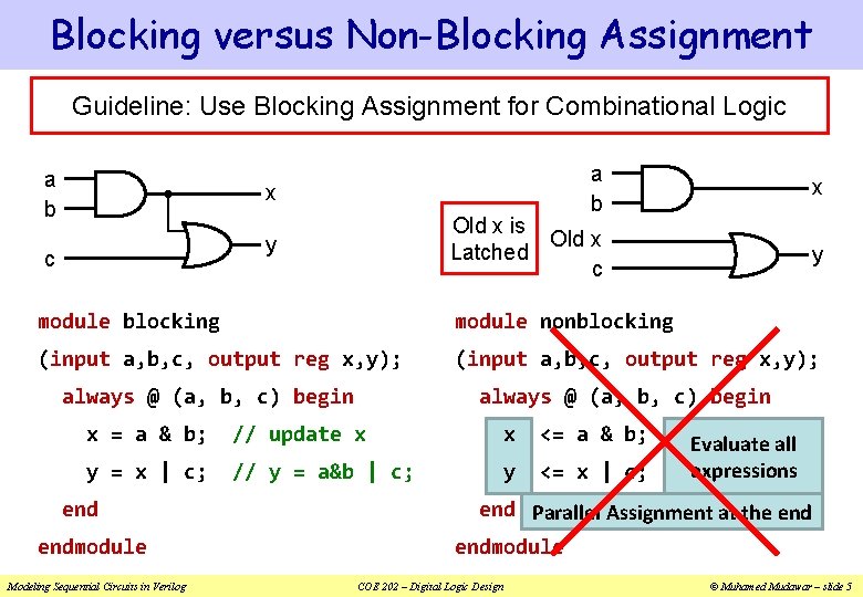
Blocking versus Non-Blocking Assignment Guideline: Use Blocking Assignment for Combinational Logic a b x Old x is Old x Latched c y c x y module blocking module nonblocking (input a, b, c, output reg x, y); always @ (a, b, c) begin x = a & b; // update x x <= a & b; y = x | c; // y = a&b | c; y <= x | c; endmodule Modeling Sequential Circuits in Verilog Evaluate all expressions end Parallel Assignment at the endmodule COE 202 – Digital Logic Design © Muhamed Mudawar – slide 5

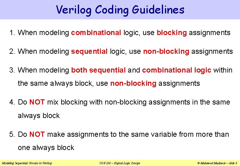
Verilog Coding Guidelines 1. When modeling combinational logic, use blocking assignments 2. When modeling sequential logic, use non-blocking assignments 3. When modeling both sequential and combinational logic within the same always block, use non-blocking assignments 4. Do NOT mix blocking with non-blocking assignments in the same always block 5. Do NOT make assignments to the same variable from more than one always block Modeling Sequential Circuits in Verilog COE 202 – Digital Logic Design © Muhamed Mudawar – slide 6

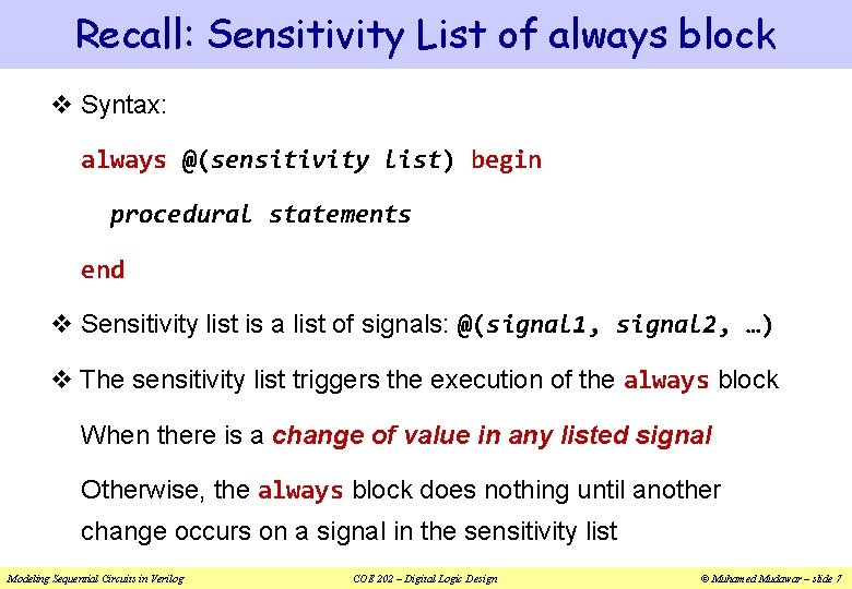
Recall: Sensitivity List of always block v Syntax: always @(sensitivity list) begin procedural statements end v Sensitivity list is a list of signals: @(signal 1, signal 2, …) v The sensitivity list triggers the execution of the always block When there is a change of value in any listed signal Otherwise, the always block does nothing until another change occurs on a signal in the sensitivity list Modeling Sequential Circuits in Verilog COE 202 – Digital Logic Design © Muhamed Mudawar – slide 7

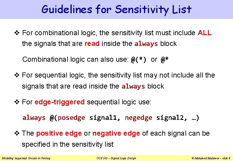
Guidelines for Sensitivity List v For combinational logic, the sensitivity list must include ALL the signals that are read inside the always block Combinational logic can also use: @(*) or @* v For sequential logic, the sensitivity list may not include all the signals that are read inside the always block v For edge-triggered sequential logic use: always @(posedge signal 1, negedge signal 2, …) v The positive edge or negative edge of each signal can be specified in the sensitivity list Modeling Sequential Circuits in Verilog COE 202 – Digital Logic Design © Muhamed Mudawar – slide 8

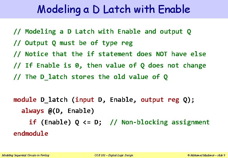
Modeling a D Latch with Enable // Modeling a D Latch with Enable and output Q // Output Q must be of type reg // Notice that the if statement does NOT have else // If Enable is 0, then value of Q does not change // The D_latch stores the old value of Q module D_latch (input D, Enable, output reg Q); always @(D, Enable) if (Enable) Q <= D; // Non-blocking assignment endmodule Modeling Sequential Circuits in Verilog COE 202 – Digital Logic Design © Muhamed Mudawar – slide 9

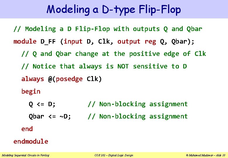
Modeling a D-type Flip-Flop // Modeling a D Flip-Flop with outputs Q and Qbar module D_FF (input D, Clk, output reg Q, Qbar); // Q and Qbar change at the positive edge of Clk // Notice that always is NOT sensitive to D always @(posedge Clk) begin Q <= D; // Non-blocking assignment Qbar <= ~D; // Non-blocking assignment endmodule Modeling Sequential Circuits in Verilog COE 202 – Digital Logic Design © Muhamed Mudawar – slide 10

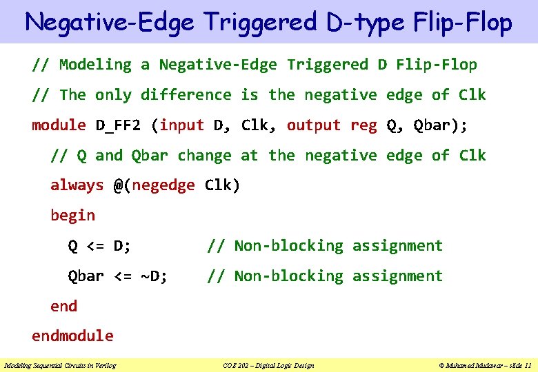
Negative-Edge Triggered D-type Flip-Flop // Modeling a Negative-Edge Triggered D Flip-Flop // The only difference is the negative edge of Clk module D_FF 2 (input D, Clk, output reg Q, Qbar); // Q and Qbar change at the negative edge of Clk always @(negedge Clk) begin Q <= D; // Non-blocking assignment Qbar <= ~D; // Non-blocking assignment endmodule Modeling Sequential Circuits in Verilog COE 202 – Digital Logic Design © Muhamed Mudawar – slide 11

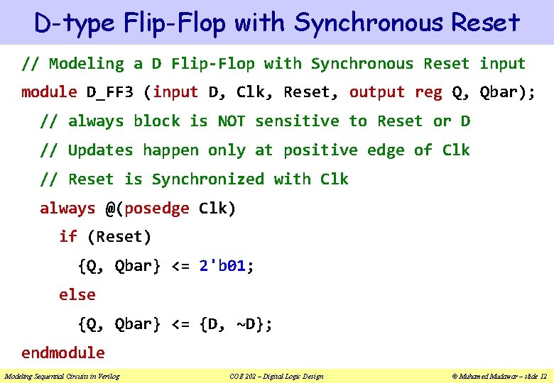
D-type Flip-Flop with Synchronous Reset // Modeling a D Flip-Flop with Synchronous Reset input module D_FF 3 (input D, Clk, Reset, output reg Q, Qbar); // always block is NOT sensitive to Reset or D // Updates happen only at positive edge of Clk // Reset is Synchronized with Clk always @(posedge Clk) if (Reset) {Q, Qbar} <= 2'b 01; else {Q, Qbar} <= {D, ~D}; endmodule Modeling Sequential Circuits in Verilog COE 202 – Digital Logic Design © Muhamed Mudawar – slide 12

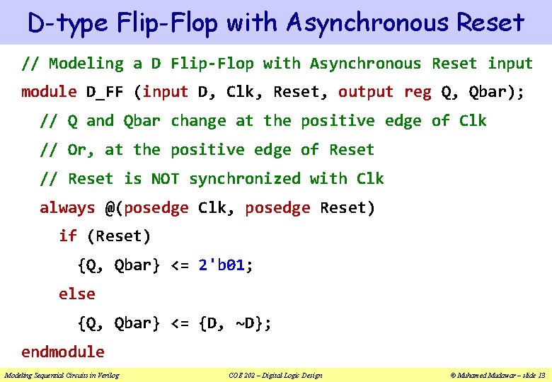
D-type Flip-Flop with Asynchronous Reset // Modeling a D Flip-Flop with Asynchronous Reset input module D_FF (input D, Clk, Reset, output reg Q, Qbar); // Q and Qbar change at the positive edge of Clk // Or, at the positive edge of Reset // Reset is NOT synchronized with Clk always @(posedge Clk, posedge Reset) if (Reset) {Q, Qbar} <= 2'b 01; else {Q, Qbar} <= {D, ~D}; endmodule Modeling Sequential Circuits in Verilog COE 202 – Digital Logic Design © Muhamed Mudawar – slide 13

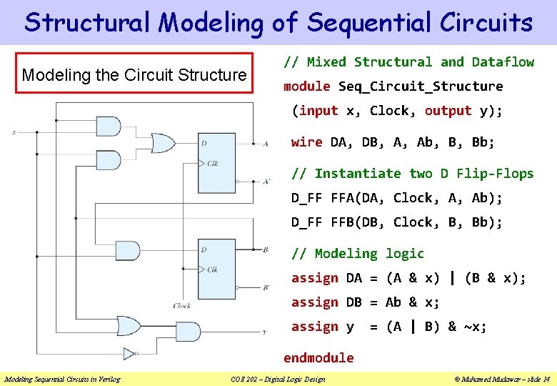
Structural Modeling of Sequential Circuits Modeling the Circuit Structure // Mixed Structural and Dataflow module Seq_Circuit_Structure (input x, Clock, output y); wire DA, DB, A, Ab, B, Bb; // Instantiate two D Flip-Flops D_FF FFA(DA, Clock, A, Ab); D_FF FFB(DB, Clock, B, Bb); // Modeling logic assign DA = (A & x) | (B & x); assign DB = Ab & x; assign y = (A | B) & ~x; endmodule Modeling Sequential Circuits in Verilog COE 202 – Digital Logic Design © Muhamed Mudawar – slide 14

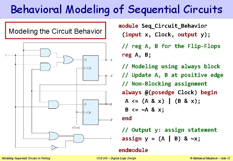
Behavioral Modeling of Sequential Circuits Modeling the Circuit Behavior module Seq_Circuit_Behavior (input x, Clock, output y); // reg A, B for the Flip-Flops reg A, B; // Modeling using always block // Update A, B at positive edge // Non-Blocking assignment always @(posedge Clock) begin A <= (A & x) | (B & x); B <= ~A & x; end // Output y: assign statement assign y = (A | B) & ~x; endmodule Modeling Sequential Circuits in Verilog COE 202 – Digital Logic Design © Muhamed Mudawar – slide 15

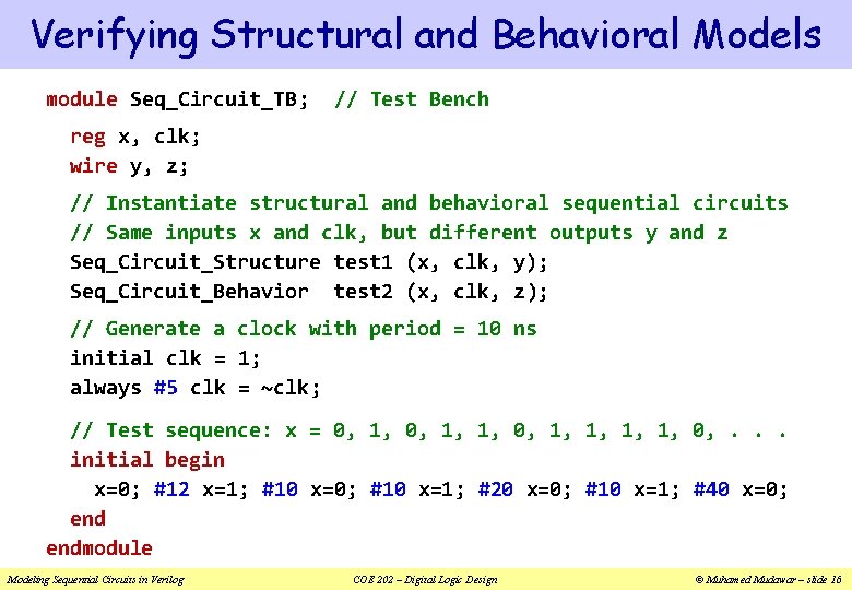
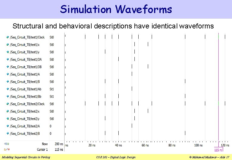
Verifying Structural and Behavioral Models module Seq_Circuit_TB; // Test Bench reg x, clk; wire y, z; // Instantiate structural and behavioral sequential circuits // Same inputs x and clk, but different outputs y and z Seq_Circuit_Structure test 1 (x, clk, y); Seq_Circuit_Behavior test 2 (x, clk, z); // Generate a clock with period = 10 ns initial clk = 1; always #5 clk = ~clk; // Test sequence: x = 0, 1, 1, 0, . . . initial begin x=0; #12 x=1; #10 x=0; #10 x=1; #20 x=0; #10 x=1; #40 x=0; endmodule Modeling Sequential Circuits in Verilog COE 202 – Digital Logic Design © Muhamed Mudawar – slide 16

Simulation Waveforms Structural and behavioral descriptions have identical waveforms Modeling Sequential Circuits in Verilog COE 202 – Digital Logic Design © Muhamed Mudawar – slide 17

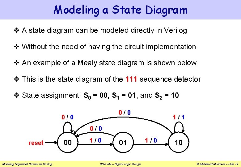
Modeling a State Diagram v A state diagram can be modeled directly in Verilog v Without the need of having the circuit implementation v An example of a Mealy state diagram is shown below v This is the state diagram of the 111 sequence detector v State assignment: S 0 = 00, S 1 = 01, and S 2 = 10 0/0 1/1 0/0 reset Modeling Sequential Circuits in Verilog 00 1/0 01 COE 202 – Digital Logic Design 1/0 10 © Muhamed Mudawar – slide 18

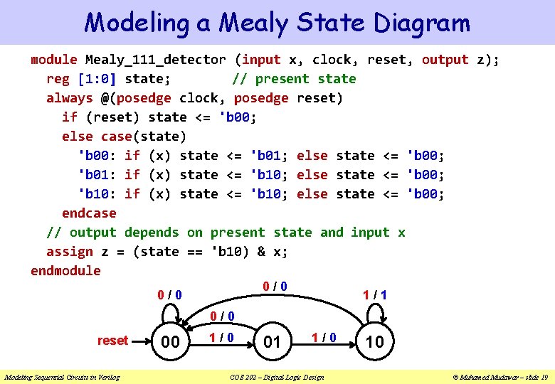
Modeling a Mealy State Diagram module Mealy_111_detector (input x, clock, reset, output z); reg [1: 0] state; // present state always @(posedge clock, posedge reset) if (reset) state <= 'b 00; else case(state) 'b 00: if (x) state <= 'b 01; else state <= 'b 00; 'b 01: if (x) state <= 'b 10; else state <= 'b 00; 'b 10: if (x) state <= 'b 10; else state <= 'b 00; endcase // output depends on present state and input x assign z = (state == 'b 10) & x; endmodule 0/0 1/1 0/0 reset Modeling Sequential Circuits in Verilog 00 1/0 01 1/0 COE 202 – Digital Logic Design 10 © Muhamed Mudawar – slide 19

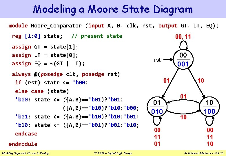
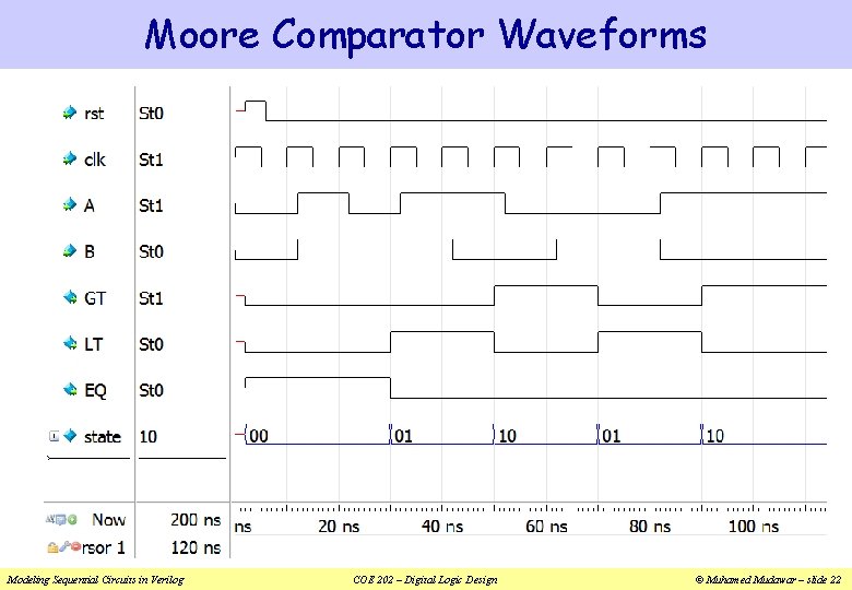
Modeling a Moore State Diagram module Moore_Comparator (input A, B, clk, rst, output GT, LT, EQ); reg [1: 0] state; // present state assign GT = state[1]; assign LT = state[0]; assign EQ = ~(GT | LT); 00 001 rst always @(posedge clk, posedge rst) if (rst) state <= 'b 00; else case (state) 'b 00: state <= ({A, B}=='b 01)? 'b 01: ({A, B}=='b 10)? 'b 10: 'b 00; 'b 01: state <= ({A, B}=='b 10)? 'b 10: 'b 01; 'b 10: state <= ({A, B}=='b 01)? 'b 01: 'b 10; endcase endmodule Modeling Sequential Circuits in Verilog 00, 11 COE 202 – Digital Logic Design 01 01 010 00 11 01 10 10 100 00 11 10 © Muhamed Mudawar – slide 20

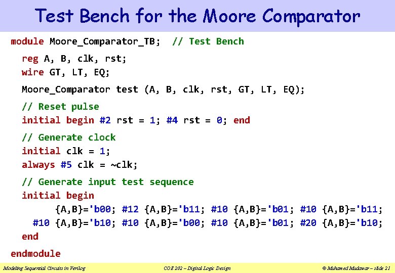
Test Bench for the Moore Comparator module Moore_Comparator_TB; // Test Bench reg A, B, clk, rst; wire GT, LT, EQ; Moore_Comparator test (A, B, clk, rst, GT, LT, EQ); // Reset pulse initial begin #2 rst = 1; #4 rst = 0; end // Generate clock initial clk = 1; always #5 clk = ~clk; // Generate input test sequence initial begin {A, B}='b 00; #12 {A, B}='b 11; #10 {A, B}='b 01; #10 {A, B}='b 10; #10 {A, B}='b 01; #20 {A, B}='b 10; endmodule Modeling Sequential Circuits in Verilog COE 202 – Digital Logic Design © Muhamed Mudawar – slide 21

Moore Comparator Waveforms Modeling Sequential Circuits in Verilog COE 202 – Digital Logic Design © Muhamed Mudawar – slide 22

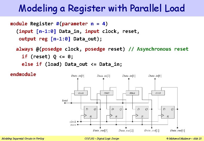
Modeling a Register with Parallel Load module Register #(parameter n = 4) (input [n-1: 0] Data_in, input clock, reset, output reg [n-1: 0] Data_out); always @(posedge clock, posedge reset) // Asynchronous reset if (reset) Q <= 0; else if (load) Data_out <= Data_in; endmodule Modeling Sequential Circuits in Verilog COE 202 – Digital Logic Design © Muhamed Mudawar – slide 23

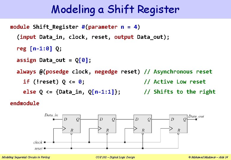
Modeling a Shift Register module Shift_Register #(parameter n = 4) (input Data_in, clock, reset, output Data_out); reg [n-1: 0] Q; assign Data_out = Q[0]; always @(posedge clock, negedge reset) // Asynchronous reset if (!reset) Q <= 0; // Active Low reset else Q <= {Data_in, Q[n-1: 1]}; // Shifts to the right endmodule Modeling Sequential Circuits in Verilog COE 202 – Digital Logic Design © Muhamed Mudawar – slide 24

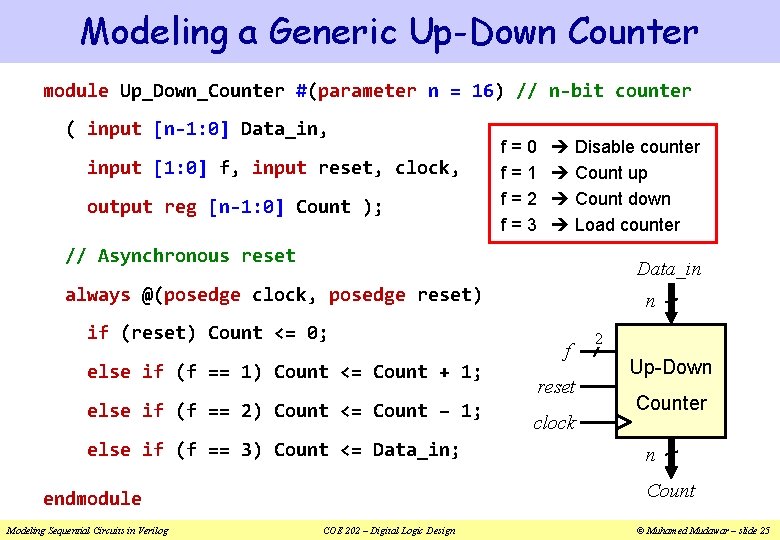
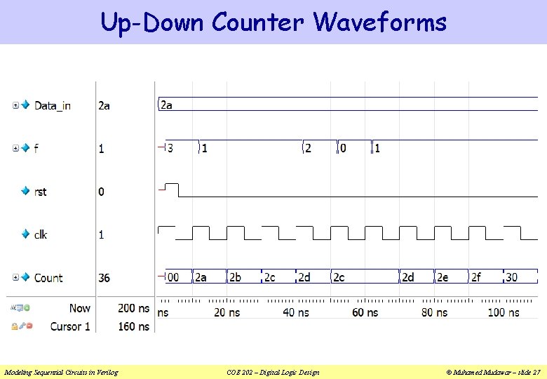
Modeling a Generic Up-Down Counter module Up_Down_Counter #(parameter n = 16) // n-bit counter ( input [n-1: 0] Data_in, input [1: 0] f, input reset, clock, output reg [n-1: 0] Count ); f=0 f=1 f=2 f=3 Disable counter Count up Count down Load counter // Asynchronous reset Data_in always @(posedge clock, posedge reset) if (reset) Count <= 0; else if (f == 1) Count <= Count + 1; else if (f == 2) Count <= Count – 1; else if (f == 3) Count <= Data_in; f reset clock 2 Up-Down Counter n Count endmodule Modeling Sequential Circuits in Verilog n COE 202 – Digital Logic Design © Muhamed Mudawar – slide 25
![Test Bench for the UpDown Counter module UpDownCounterTB Test Bench reg 7 0 Test Bench for the Up-Down Counter module Up_Down_Counter_TB; // Test Bench reg [7: 0]](https://slidetodoc.com/presentation_image_h/37d77b92db5d42e82226c4759ad03e8b/image-26.jpg)
Test Bench for the Up-Down Counter module Up_Down_Counter_TB; // Test Bench reg [7: 0] Data_in; reg [1: 0] f; reg rst, clk; wire [7: 0] Count; // Instantiate an 8 -bit test counter Up_Down_Counter #(8) test (Data_in, f, rst, clk, Count); // Initialize Data_in (in hexadecimal) initial Data_in = 8'h 2 A; // Generate reset pulse initial begin #2 rst=1; #4 rst=0; end // Generate clock initial clk = 1; always #5 clk = ~clk; // Generate function sequence initial begin #2 f=3; #10 f=1; #30 f=2; #10 f=0; #10 f=1; endmodule Modeling Sequential Circuits in Verilog COE 202 – Digital Logic Design © Muhamed Mudawar – slide 26

Up-Down Counter Waveforms Modeling Sequential Circuits in Verilog COE 202 – Digital Logic Design © Muhamed Mudawar – slide 27