Sequential Logic z Sequential Circuits y Simple circuits
- Slides: 46

Sequential Logic z Sequential Circuits y Simple circuits with feedback y Latches y Edge-triggered flip-flops z Timing Methodologies y Cascading flip-flops for properation y Clock skew z Asynchronous Inputs y Metastability and synchronization z Basic Registers y Shift registers CS 150 - Fall 2000 - Sequential Logic - 1

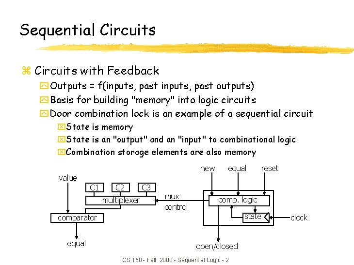
Sequential Circuits z Circuits with Feedback y Outputs = f(inputs, past outputs) y Basis for building "memory" into logic circuits y Door combination lock is an example of a sequential circuit x. State is memory x. State is an "output" and an "input" to combinational logic x. Combination storage elements are also memory new equal reset value C 1 C 2 multiplexer C 3 mux control comb. logic state comparator equal open/closed CS 150 - Fall 2000 - Sequential Logic - 2 clock

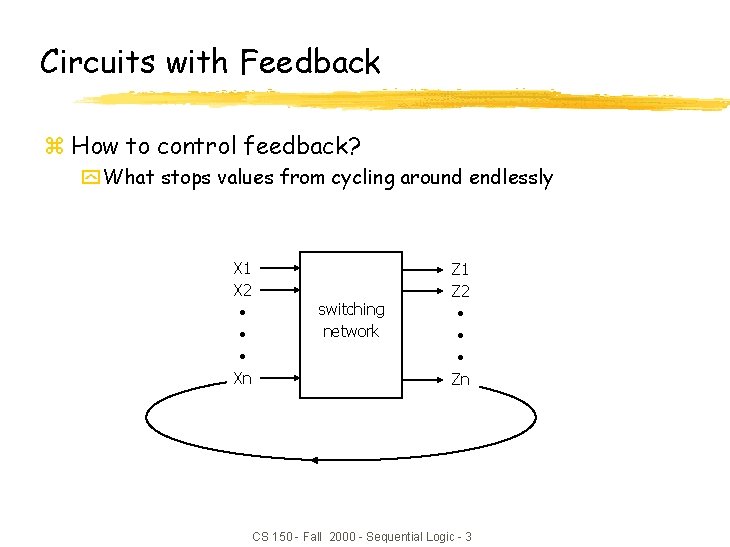
Circuits with Feedback z How to control feedback? y What stops values from cycling around endlessly X 1 X 2 • • • Xn switching network Z 1 Z 2 • • • Zn CS 150 - Fall 2000 - Sequential Logic - 3

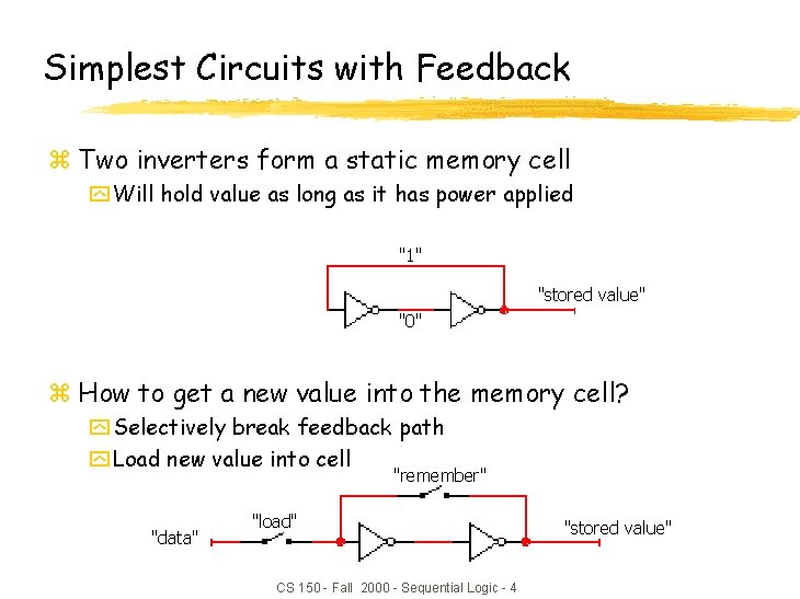
Simplest Circuits with Feedback z Two inverters form a static memory cell y Will hold value as long as it has power applied "1" "stored value" "0" z How to get a new value into the memory cell? y Selectively break feedback path y Load new value into cell "remember" "data" "load" CS 150 - Fall 2000 - Sequential Logic - 4 "stored value"

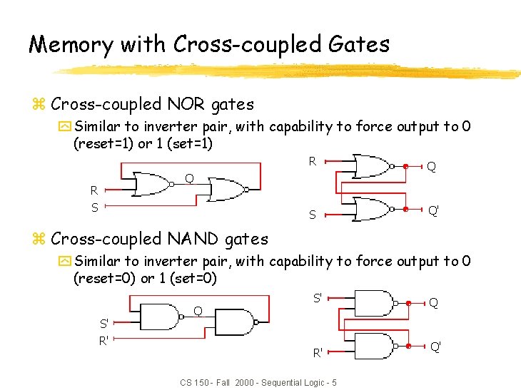
Memory with Cross-coupled Gates z Cross-coupled NOR gates y Similar to inverter pair, with capability to force output to 0 (reset=1) or 1 (set=1) R Q S Q' Q R S z Cross-coupled NAND gates y Similar to inverter pair, with capability to force output to 0 (reset=0) or 1 (set=0) S' R' Q S' R' CS 150 - Fall 2000 - Sequential Logic - 5 Q Q'

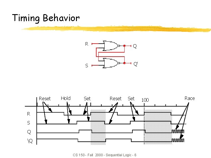
Timing Behavior Reset Hold R Q S Q' Set Reset Set R S Q Q CS 150 - Fall 2000 - Sequential Logic - 6 100 Race

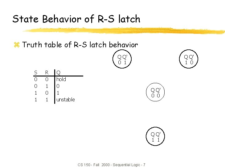
State Behavior of R-S latch z Truth table of R-S latch behavior Q Q' 0 1 S 0 0 1 1 R 0 1 Q hold 0 1 unstable Q Q' 1 0 Q Q' 0 0 Q Q' 1 1 CS 150 - Fall 2000 - Sequential Logic - 7

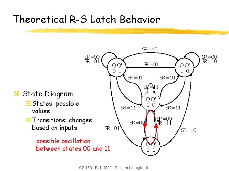
Theoretical R-S Latch Behavior SR=10 SR=01 Q Q' 0 1 SR=01 Q Q' 1 0 SR=11 z State Diagram y States: possible values y Transitions: changes based on inputs SR=11 SR=01 possible oscillation between states 00 and 11 Q Q' 0 0 SR=11 SR=00 SR=10 Q Q' 1 1 CS 150 - Fall 2000 - Sequential Logic - 8 SR=00 SR=10

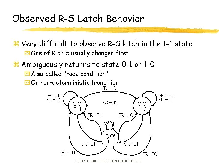
Observed R-S Latch Behavior z Very difficult to observe R-S latch in the 1 -1 state y One of R or S usually changes first z Ambiguously returns to state 0 -1 or 1 -0 y A so-called "race condition" y Or non-deterministic transition SR=10 SR=01 Q Q' 0 1 SR=01 Q Q' 1 0 SR=11 Q Q' 0 0 SR=11 SR=00 CS 150 - Fall 2000 - Sequential Logic - 9 SR=00 SR=10

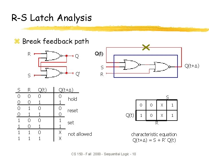
R-S Latch Analysis z Break feedback path R Q Q(t) Q(t+ ) S Q' S S 0 0 1 1 R 0 0 1 1 Q(t) 0 1 0 1 Q(t+ ) 0 hold 1 0 reset 0 1 set 1 X not allowed X R S Q(t) 0 0 X 1 1 0 X 1 R characteristic equation Q(t+ ) = S + R’ Q(t) CS 150 - Fall 2000 - Sequential Logic - 10

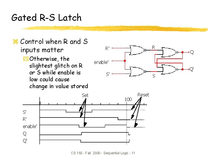
Gated R-S Latch z Control when R and S inputs matter y Otherwise, the slightest glitch on R or S while enable is low could cause change in value stored Set R R' Q enable' Q' S' S 100 S' R' enable' Q Q' CS 150 - Fall 2000 - Sequential Logic - 11 Reset

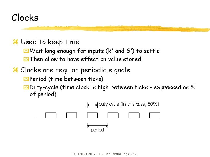
Clocks z Used to keep time y Wait long enough for inputs (R' and S') to settle y Then allow to have effect on value stored z Clocks are regular periodic signals y Period (time between ticks) y Duty-cycle (time clock is high between ticks - expressed as % of period) duty cycle (in this case, 50%) period CS 150 - Fall 2000 - Sequential Logic - 12

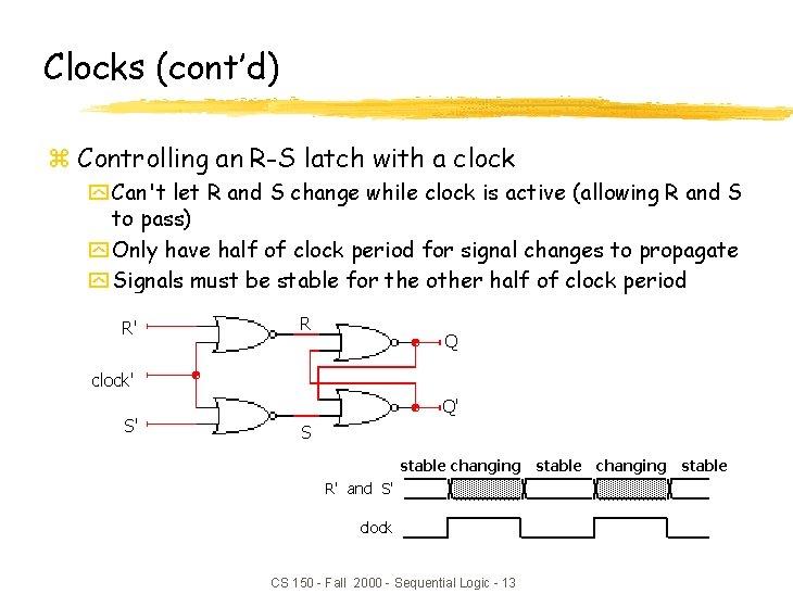
Clocks (cont’d) z Controlling an R-S latch with a clock y Can't let R and S change while clock is active (allowing R and S to pass) y Only have half of clock period for signal changes to propagate y Signals must be stable for the other half of clock period R' R Q clock' S' Q' S stable changing stable R' and S' clock CS 150 - Fall 2000 - Sequential Logic - 13

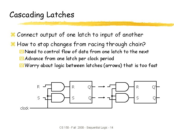
Cascading Latches z Connect output of one latch to input of another z How to stop changes from racing through chain? y Need to control flow of data from one latch to the next y Advance from one latch per clock period y Worry about logic between latches (arrows) that is too fast R R Q' S S Q clock CS 150 - Fall 2000 - Sequential Logic - 14

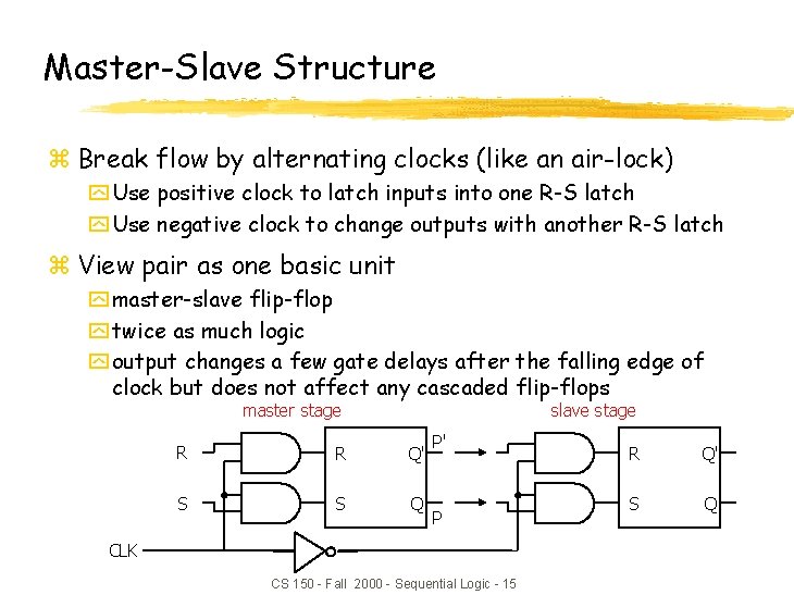
Master-Slave Structure z Break flow by alternating clocks (like an air-lock) y Use positive clock to latch inputs into one R-S latch y Use negative clock to change outputs with another R-S latch z View pair as one basic unit y master-slave flip-flop y twice as much logic y output changes a few gate delays after the falling edge of clock but does not affect any cascaded flip-flops slave stage master stage R R Q' S S Q P' P CLK CS 150 - Fall 2000 - Sequential Logic - 15 R Q' S Q

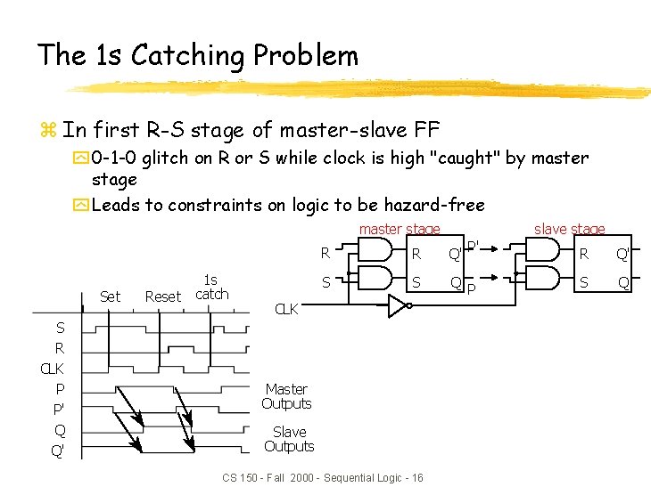
The 1 s Catching Problem z In first R-S stage of master-slave FF y 0 -1 -0 glitch on R or S while clock is high "caught" by master stage y Leads to constraints on logic to be hazard-free slave stage master stage Set S R CLK P P' Q Q' Reset 1 s catch R R Q' S S Q CLK Master Outputs Slave Outputs CS 150 - Fall 2000 - Sequential Logic - 16 P' P R Q' S Q

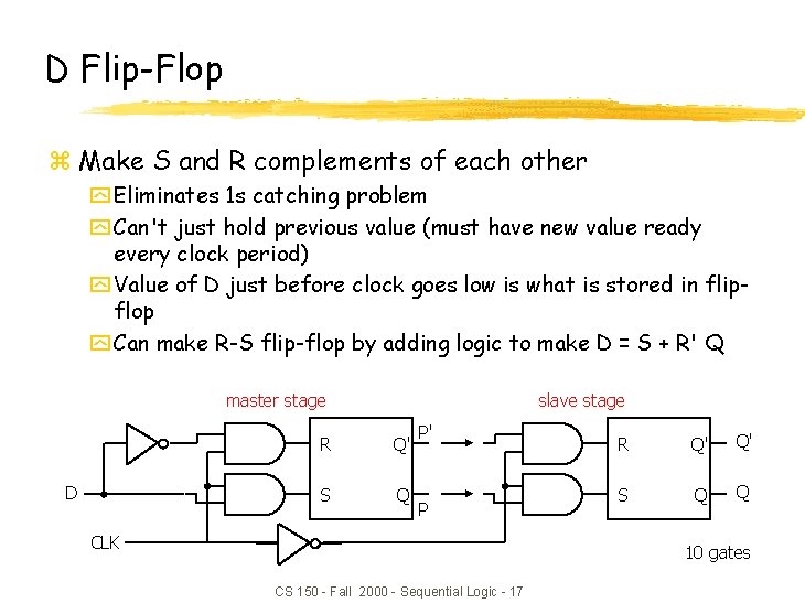
D Flip-Flop z Make S and R complements of each other y Eliminates 1 s catching problem y Can't just hold previous value (must have new value ready every clock period) y Value of D just before clock goes low is what is stored in flipflop y Can make R-S flip-flop by adding logic to make D = S + R' Q slave stage master stage D R Q' S Q P' P CLK R Q' Q' S Q Q 10 gates CS 150 - Fall 2000 - Sequential Logic - 17

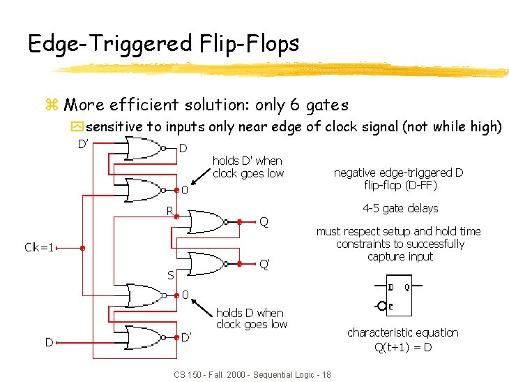
Edge-Triggered Flip-Flops z More efficient solution: only 6 gates y sensitive to inputs only near edge of clock signal (not while high) D’ D holds D' when clock goes low negative edge-triggered D flip-flop (D-FF) 0 R Q Clk=1 Q’ S 4 -5 gate delays must respect setup and hold time constraints to successfully capture input 0 holds D when clock goes low D D’ CS 150 - Fall 2000 - Sequential Logic - 18 characteristic equation Q(t+1) = D

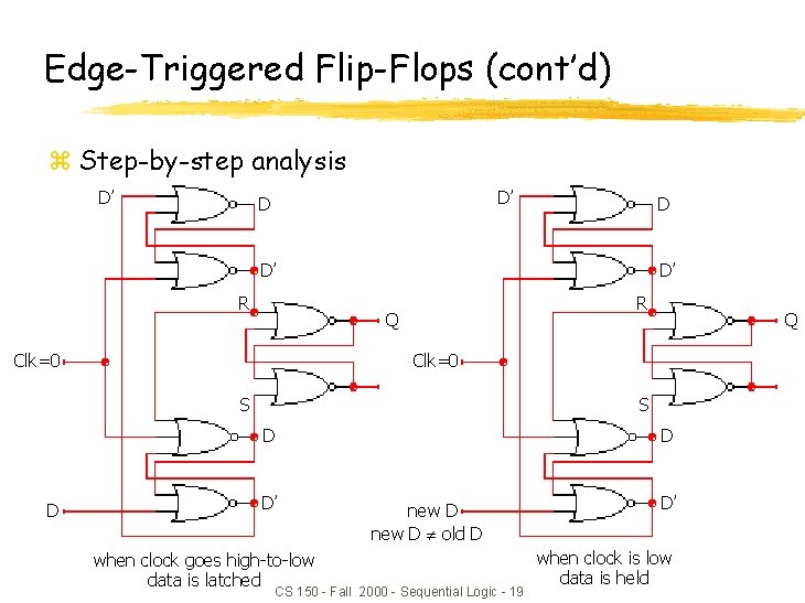
Edge-Triggered Flip-Flops (cont’d) z Step-by-step analysis D’ D’ D D D’ R Q Clk=0 S S D D Q D’ when clock goes high-to-low data is latched D new D old D CS 150 - Fall 2000 - Sequential Logic - 19 D’ when clock is low data is held

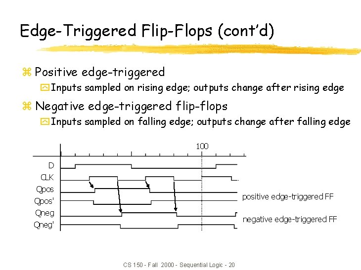
Edge-Triggered Flip-Flops (cont’d) z Positive edge-triggered y Inputs sampled on rising edge; outputs change after rising edge z Negative edge-triggered flip-flops y Inputs sampled on falling edge; outputs change after falling edge 100 D CLK Qpos' Qneg' positive edge-triggered FF negative edge-triggered FF CS 150 - Fall 2000 - Sequential Logic - 20

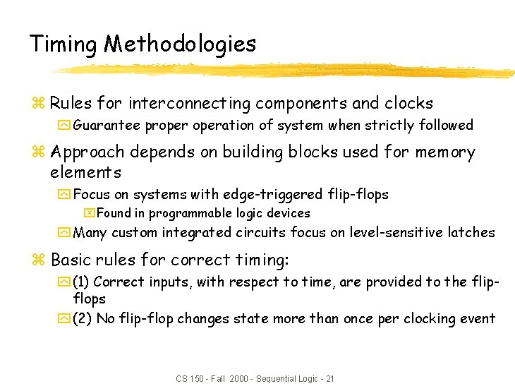
Timing Methodologies z Rules for interconnecting components and clocks y Guarantee properation of system when strictly followed z Approach depends on building blocks used for memory elements y Focus on systems with edge-triggered flip-flops x. Found in programmable logic devices y Many custom integrated circuits focus on level-sensitive latches z Basic rules for correct timing: y (1) Correct inputs, with respect to time, are provided to the flipflops y (2) No flip-flop changes state more than once per clocking event CS 150 - Fall 2000 - Sequential Logic - 21

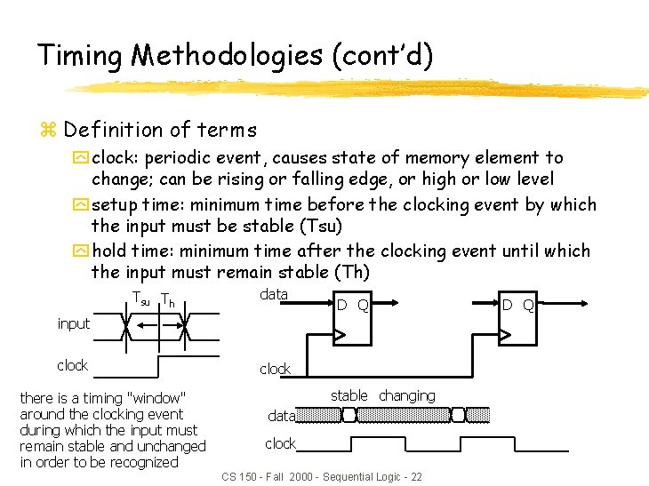
Timing Methodologies (cont’d) z Definition of terms y clock: periodic event, causes state of memory element to change; can be rising or falling edge, or high or low level y setup time: minimum time before the clocking event by which the input must be stable (Tsu) y hold time: minimum time after the clocking event until which the input must remain stable (Th) Tsu Th data D Q input clock there is a timing "window" around the clocking event during which the input must remain stable and unchanged in order to be recognized clock stable changing data clock CS 150 - Fall 2000 - Sequential Logic - 22 D Q

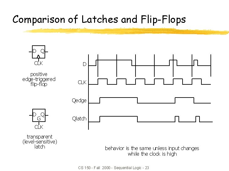
Comparison of Latches and Flip-Flops D Q CLK positive edge-triggered flip-flop D CLK Qedge D Q G Qlatch CLK transparent (level-sensitive) latch behavior is the same unless input changes while the clock is high CS 150 - Fall 2000 - Sequential Logic - 23

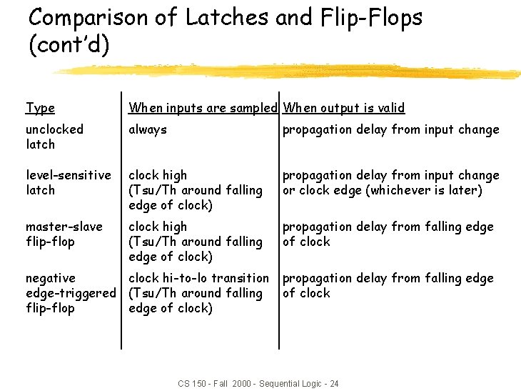
Comparison of Latches and Flip-Flops (cont’d) Type When inputs are sampled When output is valid unclocked latch always propagation delay from input change level-sensitive latch clock high (Tsu/Th around falling edge of clock) propagation delay from input change or clock edge (whichever is later) master-slave flip-flop clock high (Tsu/Th around falling edge of clock) propagation delay from falling edge of clock negative clock hi-to-lo transition propagation delay from falling edge-triggered (Tsu/Th around falling of clock flip-flop edge of clock) CS 150 - Fall 2000 - Sequential Logic - 24

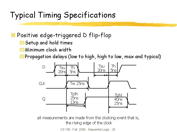
Typical Timing Specifications z Positive edge-triggered D flip-flop y Setup and hold times y Minimum clock width y Propagation delays (low to high, high to low, max and typical) D CLK Q Tsu Th 20 ns 5 ns Tsu 20 ns Th 5 ns Tw 25 ns Tplh 25 ns 13 ns Tphl 40 ns 25 ns all measurements are made from the clocking event that is, the rising edge of the clock CS 150 - Fall 2000 - Sequential Logic - 25

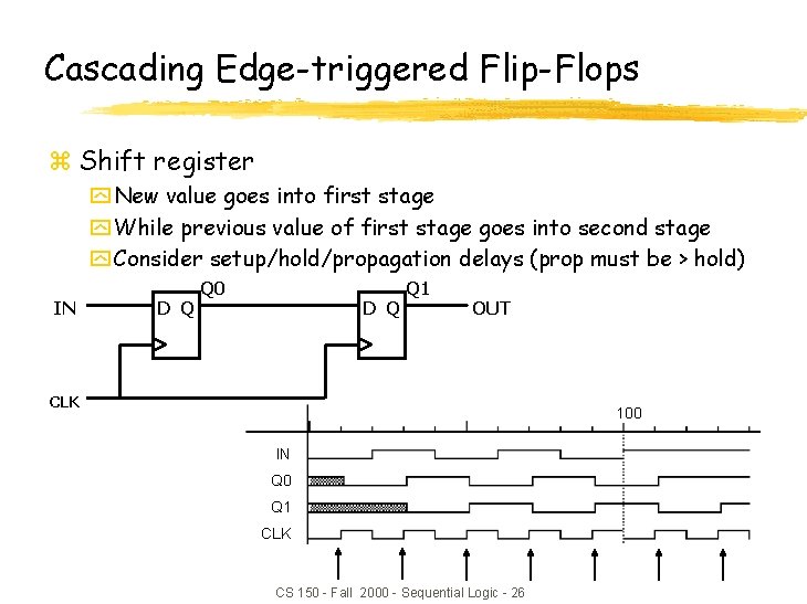
Cascading Edge-triggered Flip-Flops z Shift register y New value goes into first stage y While previous value of first stage goes into second stage y Consider setup/hold/propagation delays (prop must be > hold) IN D Q Q 0 D Q Q 1 OUT CLK 100 IN Q 0 Q 1 CLK CS 150 - Fall 2000 - Sequential Logic - 26

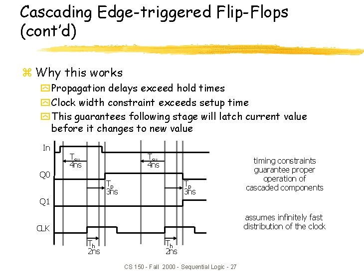
Cascading Edge-triggered Flip-Flops (cont’d) z Why this works y Propagation delays exceed hold times y Clock width constraint exceeds setup time y This guarantees following stage will latch current value before it changes to new value In Tsu 4 ns Q 0 Tp 3 ns timing constraints guarantee properation of cascaded components Q 1 assumes infinitely fast distribution of the clock CLK Th 2 ns CS 150 - Fall 2000 - Sequential Logic - 27

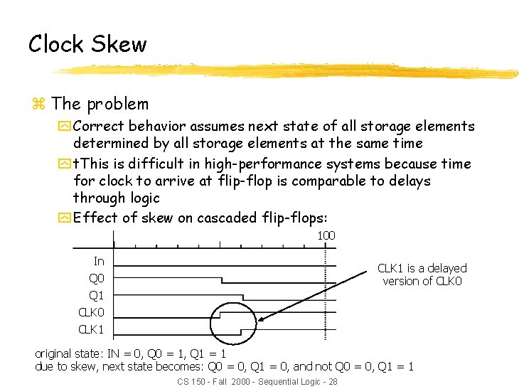
Clock Skew z The problem y Correct behavior assumes next state of all storage elements determined by all storage elements at the same time y t. This is difficult in high-performance systems because time for clock to arrive at flip-flop is comparable to delays through logic y Effect of skew on cascaded flip-flops: 100 In Q 0 Q 1 CLK 0 CLK 1 is a delayed version of CLK 0 original state: IN = 0, Q 0 = 1, Q 1 = 1 due to skew, next state becomes: Q 0 = 0, Q 1 = 0, and not Q 0 = 0, Q 1 = 1 CS 150 - Fall 2000 - Sequential Logic - 28

Summary of Latches and Flip-Flops z Development of D-FF y Level-sensitive used in custom integrated circuits xcan be made with 4 switches y Edge-triggered used in programmable logic devices y Good choice for data storage register z Historically J-K FF was popular but now never used y Similar to R-S but with 1 -1 being used to toggle output (complement state) y Good in days of TTL/SSI (more complex input function: D = JQ' + K'Q y Not a good choice for PALs/PLAs as it requires 2 inputs y Can always be implemented using D-FF z Preset and clear inputs are highly desirable on flip-flops y Used at start-up or to reset system to a known state CS 150 - Fall 2000 - Sequential Logic - 29

Metastability and Asynchronous inputs z Clocked synchronous circuits y Inputs, state, and outputs sampled or changed in relation to a common reference signal (called the clock) y E. g. , master/slave, edge-triggered z Asynchronous circuits y Inputs, state, and outputs sampled or changed independently of a common reference signal (glitches/hazards a major concern) y E. g. , R-S latch z Asynchronous inputs to synchronous circuits y Inputs can change at any time, will not meet setup/hold times y Dangerous, synchronous inputs are greatly preferred y Cannot be avoided (e. g. , reset signal, memory wait, user input) CS 150 - Fall 2000 - Sequential Logic - 30

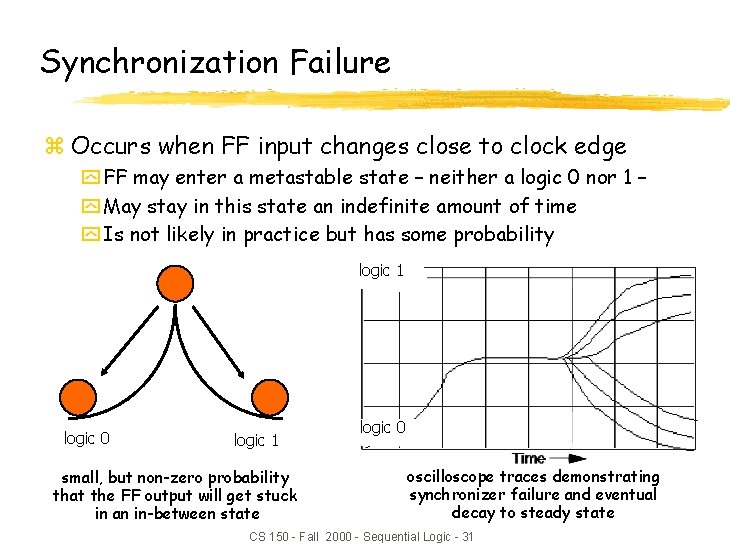
Synchronization Failure z Occurs when FF input changes close to clock edge y FF may enter a metastable state – neither a logic 0 nor 1 – y May stay in this state an indefinite amount of time y Is not likely in practice but has some probability logic 1 logic 0 logic 1 small, but non-zero probability that the FF output will get stuck in an in-between state logic 0 oscilloscope traces demonstrating synchronizer failure and eventual decay to steady state CS 150 - Fall 2000 - Sequential Logic - 31

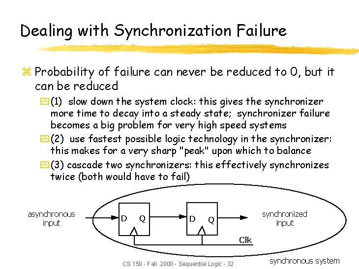
Dealing with Synchronization Failure z Probability of failure can never be reduced to 0, but it can be reduced y (1) slow down the system clock: this gives the synchronizer more time to decay into a steady state; synchronizer failure becomes a big problem for very high speed systems y (2) use fastest possible logic technology in the synchronizer: this makes for a very sharp "peak" upon which to balance y (3) cascade two synchronizers: this effectively synchronizes twice (both would have to fail) asynchronous input D Q D synchronized input Q Clk CS 150 - Fall 2000 - Sequential Logic - 32 synchronous system

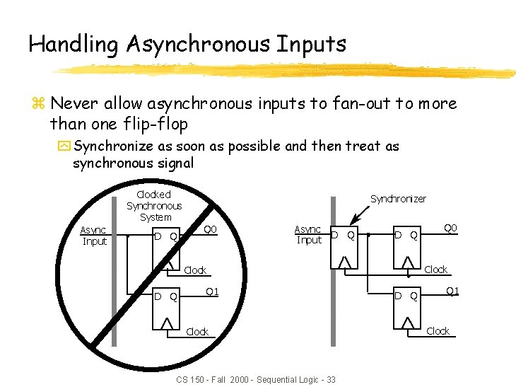
Handling Asynchronous Inputs z Never allow asynchronous inputs to fan-out to more than one flip-flop y Synchronize as soon as possible and then treat as synchronous signal Clocked Synchronous System Async Input D Q Synchronizer Q 0 Async Input D Q Clock D Q Q 1 Clock CS 150 - Fall 2000 - Sequential Logic - 33 Q 0 D Q Q 1 Clock

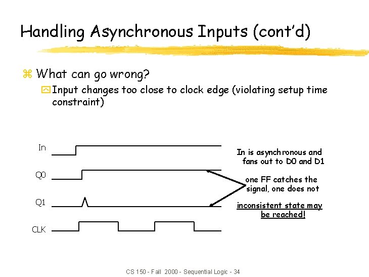
Handling Asynchronous Inputs (cont’d) z What can go wrong? y Input changes too close to clock edge (violating setup time constraint) In In is asynchronous and fans out to D 0 and D 1 Q 0 one FF catches the signal, one does not Q 1 inconsistent state may be reached! CLK CS 150 - Fall 2000 - Sequential Logic - 34

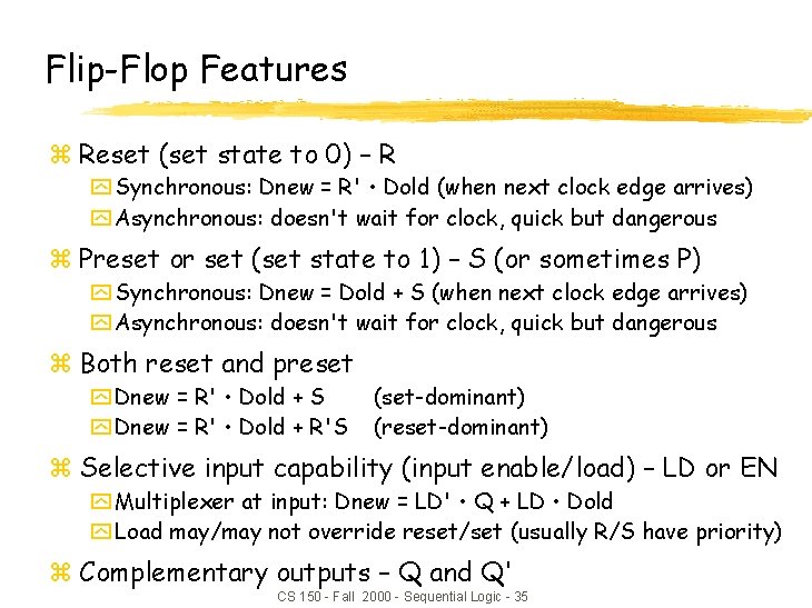
Flip-Flop Features z Reset (set state to 0) – R y Synchronous: Dnew = R' • Dold (when next clock edge arrives) y Asynchronous: doesn't wait for clock, quick but dangerous z Preset or set (set state to 1) – S (or sometimes P) y Synchronous: Dnew = Dold + S (when next clock edge arrives) y Asynchronous: doesn't wait for clock, quick but dangerous z Both reset and preset y Dnew = R' • Dold + S y Dnew = R' • Dold + R'S (set-dominant) (reset-dominant) z Selective input capability (input enable/load) – LD or EN y Multiplexer at input: Dnew = LD' • Q + LD • Dold y Load may/may not override reset/set (usually R/S have priority) z Complementary outputs – Q and Q' CS 150 - Fall 2000 - Sequential Logic - 35

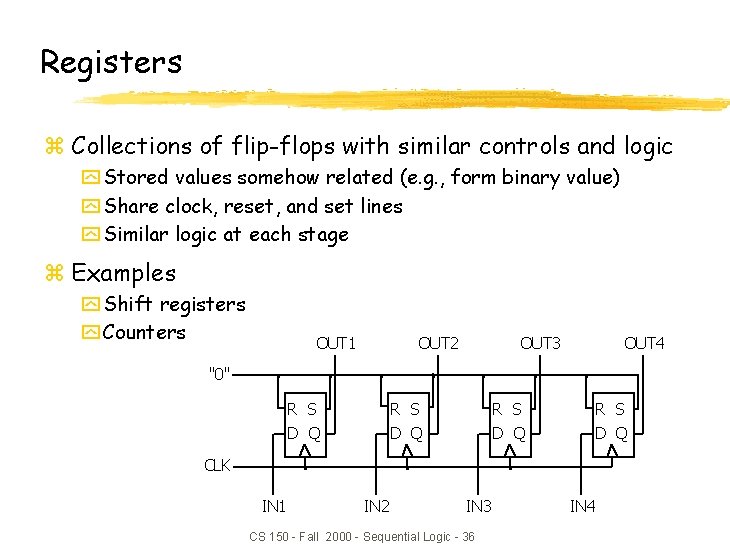
Registers z Collections of flip-flops with similar controls and logic y Stored values somehow related (e. g. , form binary value) y Share clock, reset, and set lines y Similar logic at each stage z Examples y Shift registers y Counters OUT 1 OUT 2 OUT 3 OUT 4 "0" R S R S D Q D Q CLK IN 1 IN 2 IN 3 CS 150 - Fall 2000 - Sequential Logic - 36 IN 4

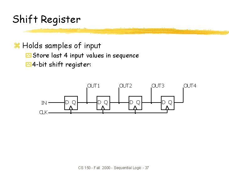
Shift Register z Holds samples of input y Store last 4 input values in sequence y 4 -bit shift register: OUT 1 IN D Q OUT 2 D Q CLK CS 150 - Fall 2000 - Sequential Logic - 37 OUT 3 D Q OUT 4

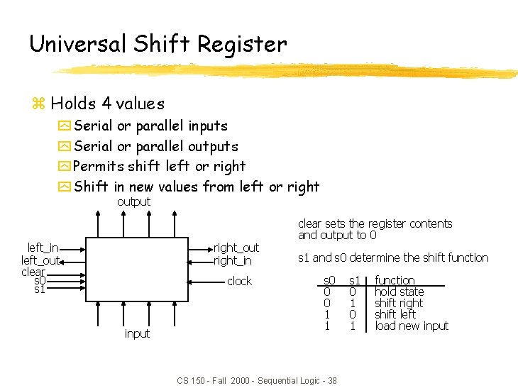
Universal Shift Register z Holds 4 values y Serial or parallel inputs y Serial or parallel outputs y Permits shift left or right y Shift in new values from left or right output left_in left_out clear s 0 s 1 right_out right_in clock input clear sets the register contents and output to 0 s 1 and s 0 determine the shift function s 0 0 0 1 1 CS 150 - Fall 2000 - Sequential Logic - 38 s 1 0 1 function hold state shift right shift left load new input

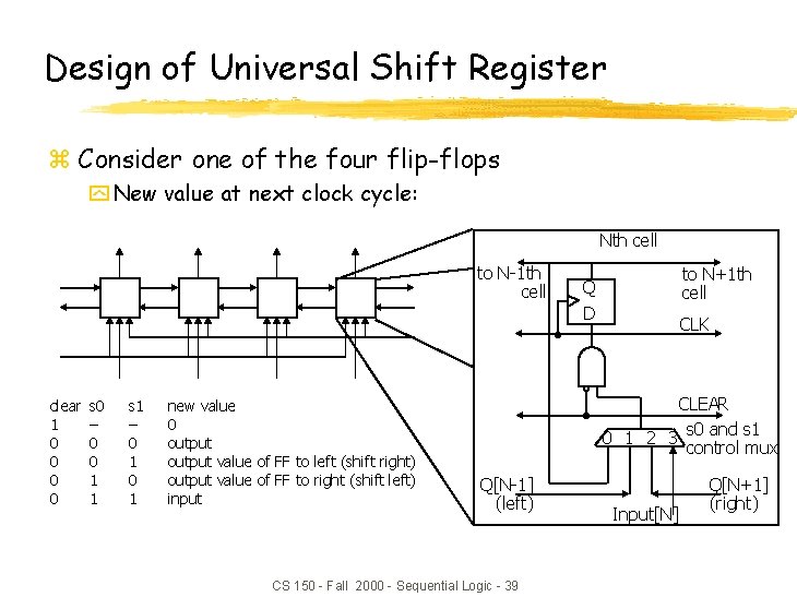
Design of Universal Shift Register z Consider one of the four flip-flops y New value at next clock cycle: Nth cell to N-1 th cell clear 1 0 0 s 0 – 0 0 1 1 s 1 – 0 1 new value 0 output value of FF to left (shift right) output value of FF to right (shift left) input to N+1 th cell Q D CLK CLEAR 0 1 2 3 s 0 and s 1 control mux Q[N-1] (left) CS 150 - Fall 2000 - Sequential Logic - 39 Input[N] Q[N+1] (right)

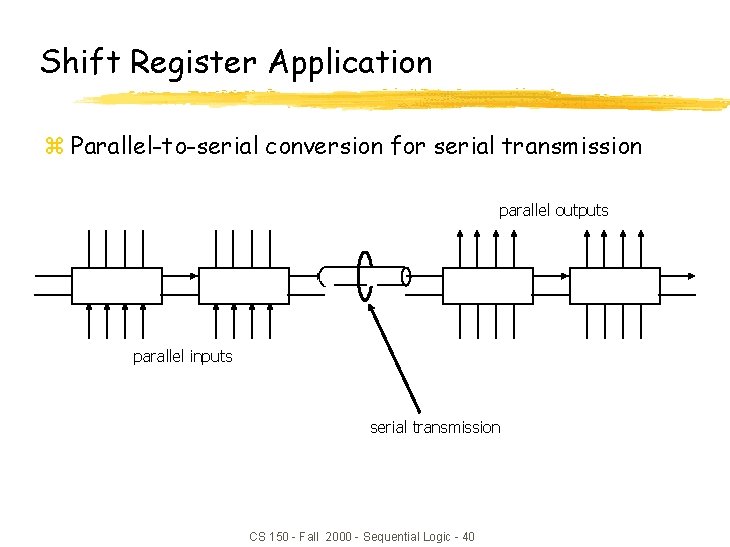
Shift Register Application z Parallel-to-serial conversion for serial transmission parallel outputs parallel inputs serial transmission CS 150 - Fall 2000 - Sequential Logic - 40

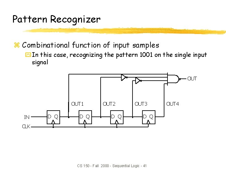
Pattern Recognizer z Combinational function of input samples y In this case, recognizing the pattern 1001 on the single input signal OUT 1 IN D Q OUT 2 D Q OUT 3 D Q CLK CS 150 - Fall 2000 - Sequential Logic - 41 OUT 4

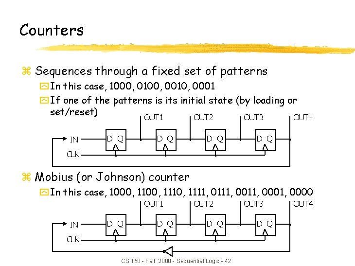
Counters z Sequences through a fixed set of patterns y In this case, 1000, 0100, 0010, 0001 y If one of the patterns is its initial state (by loading or set/reset) OUT 1 IN D Q OUT 2 D Q OUT 3 OUT 4 D Q CLK z Mobius (or Johnson) counter y In this case, 1000, 1110, 1111, 0011, 0000 OUT 1 IN D Q OUT 2 D Q CLK CS 150 - Fall 2000 - Sequential Logic - 42 OUT 3 D Q OUT 4

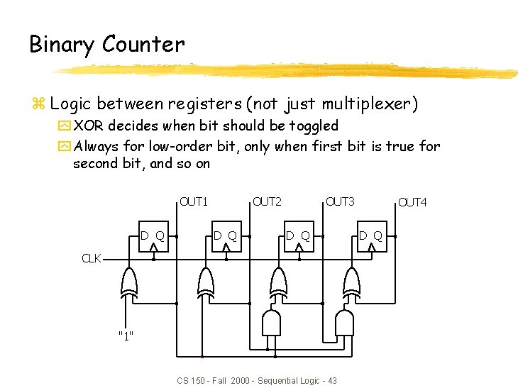
Binary Counter z Logic between registers (not just multiplexer) y XOR decides when bit should be toggled y Always for low-order bit, only when first bit is true for second bit, and so on OUT 1 D Q OUT 2 D Q OUT 3 D Q CLK "1" CS 150 - Fall 2000 - Sequential Logic - 43 OUT 4 D Q

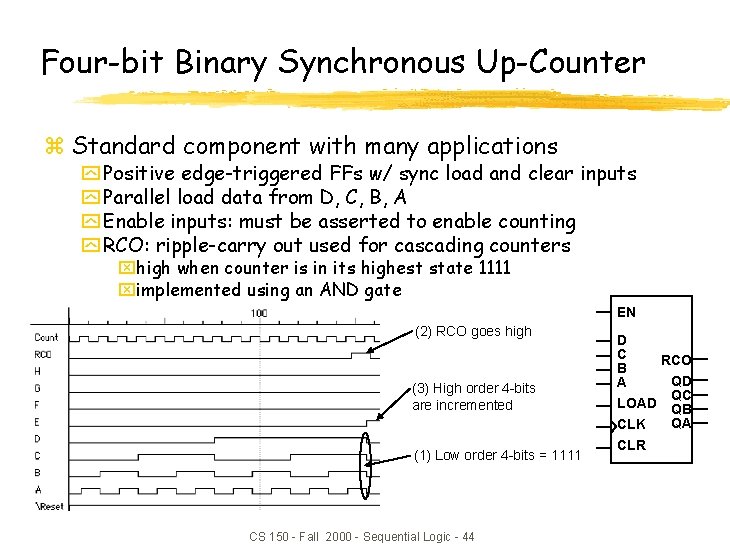
Four-bit Binary Synchronous Up-Counter z Standard component with many applications y Positive edge-triggered FFs w/ sync load and clear inputs y Parallel load data from D, C, B, A y Enable inputs: must be asserted to enable counting y RCO: ripple-carry out used for cascading counters xhigh when counter is in its highest state 1111 ximplemented using an AND gate EN (2) RCO goes high (3) High order 4 -bits are incremented (1) Low order 4 -bits = 1111 CS 150 - Fall 2000 - Sequential Logic - 44 D C RCO B QD A QC LOAD QB QA CLK CLR

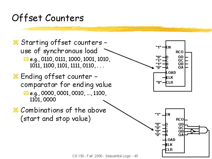
Offset Counters z Starting offset counters – use of synchronous load y e. g. , 0110, 0111, 1000, 1001, 1010, 1011, 1100, 1101, 1111, 0110, . . . z Ending offset counter – comparator for ending value "1" "0" EN RCO QD QC QB QA D C B A LOAD CLK CLR y e. g. , 0000, 0001, 0010, . . . , 1100, 1101, 0000 z Combinations of the above (start and stop value) CS 150 - Fall 2000 - Sequential Logic - 45 "1" "0" "0" EN D C B A LOAD CLK CLR RCO QD QC QB QA

Sequential Logic Summary z Fundamental building block of circuits with state y Latch and flip-flop y R-S latch, R-S master/slave, D master/slave, edge-triggered D FF z Timing methodologies y Use of clocks y Cascaded FFs work because prop delays exceed hold times y Beware of clock skew z Asynchronous inputs and their dangers y Synchronizer failure: what it is and how to minimize its impact z Basic registers y Shift registers y Pattern detectors y Counters CS 150 - Fall 2000 - Sequential Logic - 46