Modular Sequential Circuits COE 202 Digital Logic Design





- Slides: 37

Modular Sequential Circuits COE 202 Digital Logic Design Dr. Muhamed Mudawar King Fahd University of Petroleum and Minerals

Presentation Outline v Registers v Shift Registers and their Applications v Ripple Counters v Synchronous Counters v Memory and ROM Modular Sequential Circuits COE 202 – Digital Logic Design © Muhamed Mudawar – slide 2

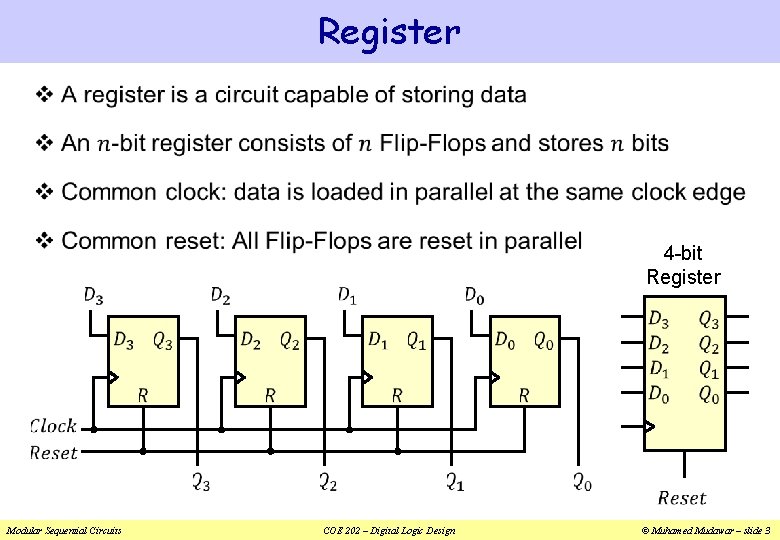
Register v 4 -bit Register Modular Sequential Circuits COE 202 – Digital Logic Design © Muhamed Mudawar – slide 3

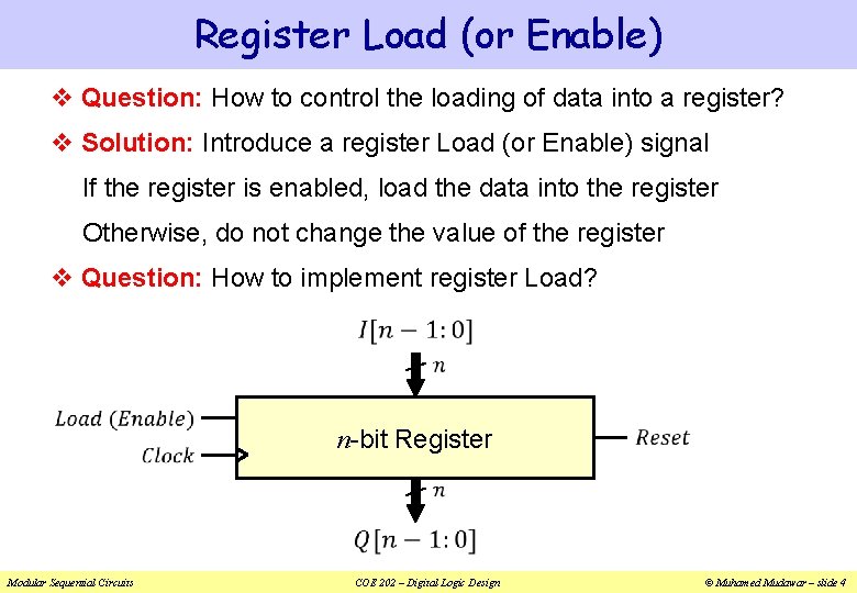
Register Load (or Enable) v Question: How to control the loading of data into a register? v Solution: Introduce a register Load (or Enable) signal If the register is enabled, load the data into the register Otherwise, do not change the value of the register v Question: How to implement register Load? n-bit Register Modular Sequential Circuits COE 202 – Digital Logic Design © Muhamed Mudawar – slide 4

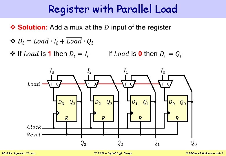
Register with Parallel Load v 1 0 1 0 Modular Sequential Circuits COE 202 – Digital Logic Design © Muhamed Mudawar – slide 5

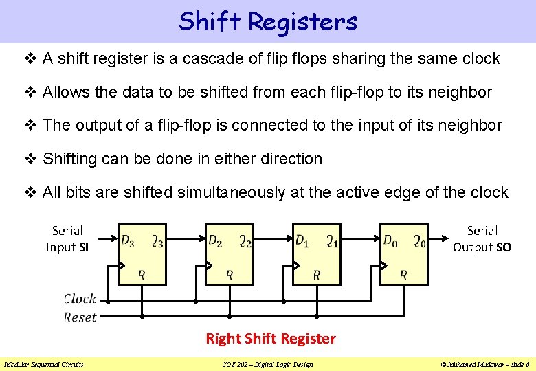
Shift Registers v A shift register is a cascade of flip flops sharing the same clock v Allows the data to be shifted from each flip-flop to its neighbor v The output of a flip-flop is connected to the input of its neighbor v Shifting can be done in either direction v All bits are shifted simultaneously at the active edge of the clock Serial Input SI Serial Output SO Right Shift Register Modular Sequential Circuits COE 202 – Digital Logic Design © Muhamed Mudawar – slide 6

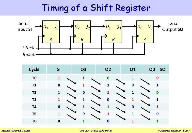
Timing of a Shift Register Serial Input SI Serial Output SO Cycle SI Q 3 Q 2 Q 1 Q 0 = SO T 0 1 1 0 T 1 0 1 T 2 1 0 1 1 0 T 3 1 1 0 1 1 T 4 0 1 1 0 1 T 5 1 0 1 1 0 T 6 0 1 1 Modular Sequential Circuits COE 202 – Digital Logic Design © Muhamed Mudawar – slide 7

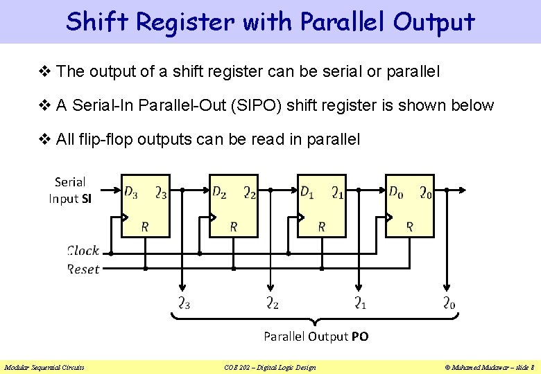
Shift Register with Parallel Output v The output of a shift register can be serial or parallel v A Serial-In Parallel-Out (SIPO) shift register is shown below v All flip-flop outputs can be read in parallel Serial Input SI Parallel Output PO Modular Sequential Circuits COE 202 – Digital Logic Design © Muhamed Mudawar – slide 8

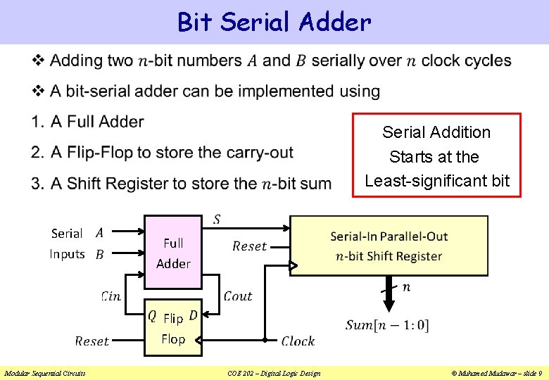
Bit Serial Adder v Serial Addition Starts at the Least-significant bit Serial Inputs Full Adder Flip Modular Sequential Circuits Flop COE 202 – Digital Logic Design © Muhamed Mudawar – slide 9

Sequence Detector with a Shift Register v A sequence detector can be implemented using: Left Shift Register (SIPO) + AND Gates v Example: Detecting the sequences 1010 and 1100 Bits are shifted left starting at the most-significant bit 1 0 1 0 Serial Input SI Detect 1010 Detect 1100 Modular Sequential Circuits COE 202 – Digital Logic Design © Muhamed Mudawar – slide 10

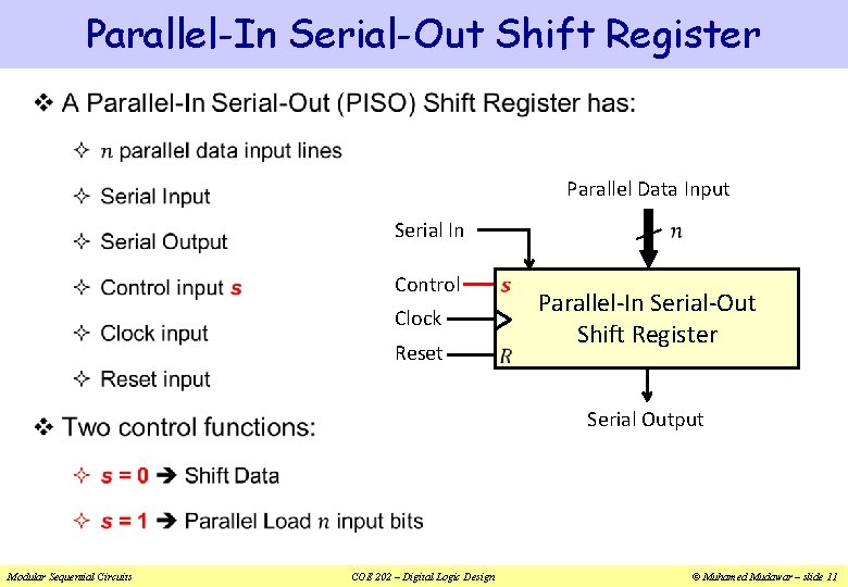
Parallel-In Serial-Out Shift Register v Parallel Data Input Serial In Control Clock Reset Parallel-In Serial-Out Shift Register Serial Output Modular Sequential Circuits COE 202 – Digital Logic Design © Muhamed Mudawar – slide 11

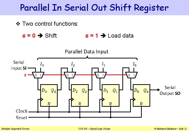
Parallel In Serial Out Shift Register v Two control functions: s = 0 Shift s = 1 Load data Parallel Data Input Serial Input SI 0 1 0 1 0 1 Serial Output SO Modular Sequential Circuits COE 202 – Digital Logic Design © Muhamed Mudawar – slide 12

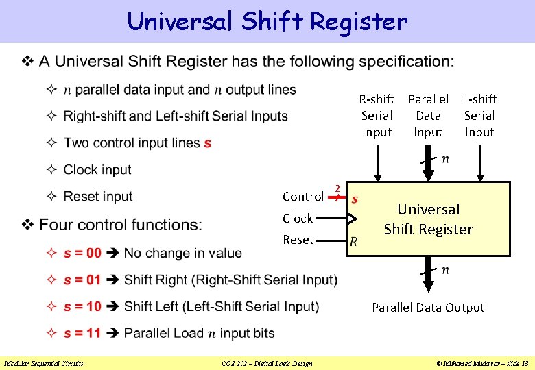
Universal Shift Register v R-shift Parallel L-shift Serial Data Serial Input Control 2 Clock Reset Universal Shift Register Parallel Data Output Modular Sequential Circuits COE 202 – Digital Logic Design © Muhamed Mudawar – slide 13

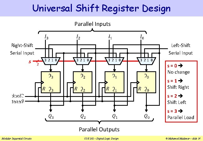
Universal Shift Register Design Parallel Inputs Right-Shift Serial Input Left-Shift Serial Input 2 3210 s=0 No change s=1 Shift Right s=2 Shift Left s=3 Parallel Load Parallel Outputs Modular Sequential Circuits COE 202 – Digital Logic Design © Muhamed Mudawar – slide 14

Counter v Sequential circuit that goes through a specific sequence of states v Output of the counter is the count value v Modulo-N counter: goes through 0, 1, 2, …, (N – 1) v Modulo-8 binary counter: goes through 0, 1, 2, …, 7 v Modulo-10 (BCD) counter: goes through 0, 1, 2, …, 9 v Counting can be up or down v Some Applications: ² Timers Counter ² Event Counting ² Frequency Division Modular Sequential Circuits n COE 202 – Digital Logic Design © Muhamed Mudawar – slide 15

Implementing Counters Two Basic Approaches: 1. Ripple Counters ² The system clock is connected to the clock input of the first flip-flop (LSB) ² Each flip-flop output connects to the clock input of the next flip-flop ² Advantage: simple circuit and low power consumption ² Disadvantage: The counter is not truly synchronous ² No common clock to all flip-flops ² Ripple propagation delay as the clock signal propagates to the MSB 2. Synchronous Counters ² The system clock is connected to the clock input of ALL flip-flops ² Combinational logic is used to implement the desired state sequence Modular Sequential Circuits COE 202 – Digital Logic Design © Muhamed Mudawar – slide 16

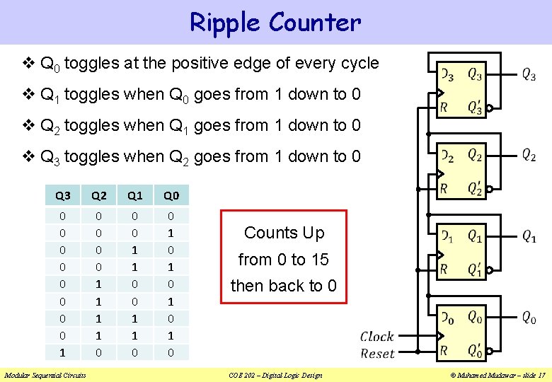
Ripple Counter v Q 0 toggles at the positive edge of every cycle v Q 1 toggles when Q 0 goes from 1 down to 0 v Q 2 toggles when Q 1 goes from 1 down to 0 v Q 3 toggles when Q 2 goes from 1 down to 0 Q 3 Q 2 Q 1 Q 0 0 0 0 0 1 1 0 0 0 1 1 0 0 1 0 1 0 Modular Sequential Circuits Counts Up from 0 to 15 then back to 0 COE 202 – Digital Logic Design © Muhamed Mudawar – slide 17

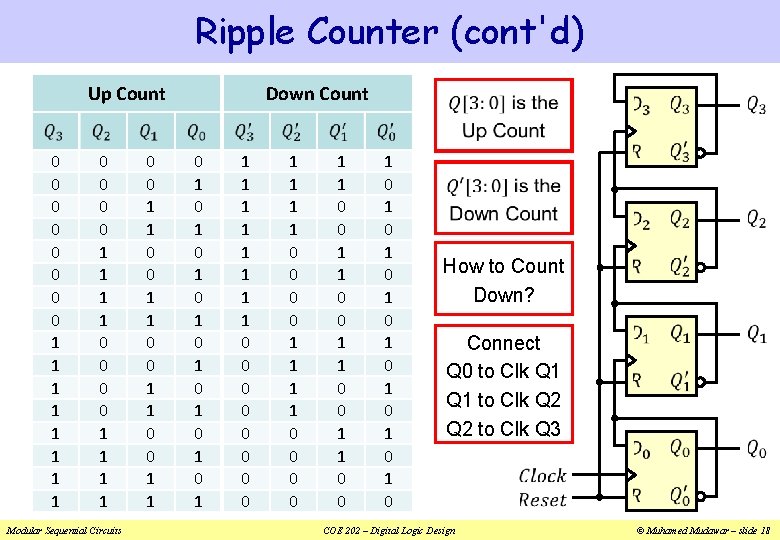
Ripple Counter (cont'd) Up Count 0 0 0 0 1 1 1 1 Modular Sequential Circuits 0 0 1 1 Down Count 0 1 0 1 1 1 1 1 0 0 0 0 1 1 0 0 1 0 1 0 How to Count Down? Connect Q 0 to Clk Q 1 to Clk Q 2 to Clk Q 3 COE 202 – Digital Logic Design © Muhamed Mudawar – slide 18

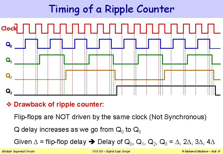
Timing of a Ripple Counter Clock Q 0 Q 1 Q 2 Q 3 v Drawback of ripple counter: Flip-flops are NOT driven by the same clock (Not Synchronous) Q delay increases as we go from Q 0 to Q 3 Given = flip-flop delay Delay of Q 0, Q 1, Q 2, Q 3 = , 2 , 3 , 4 Modular Sequential Circuits COE 202 – Digital Logic Design © Muhamed Mudawar – slide 19

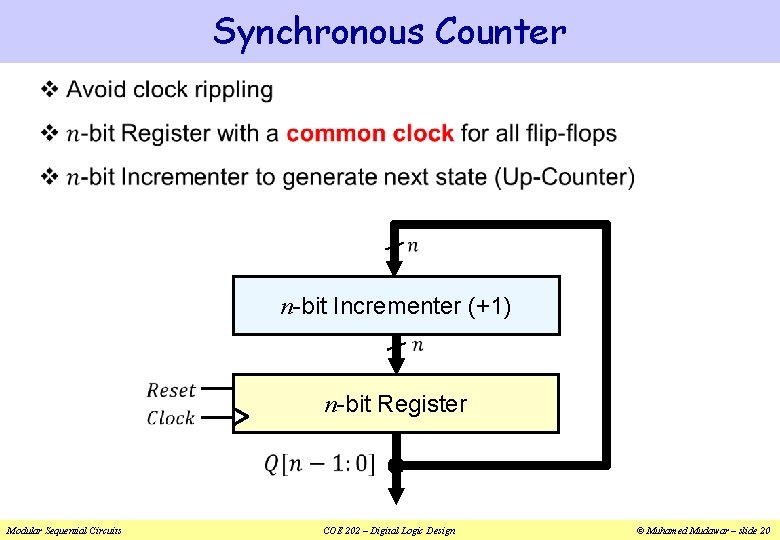
Synchronous Counter v n-bit Incrementer (+1) n-bit Register Modular Sequential Circuits COE 202 – Digital Logic Design © Muhamed Mudawar – slide 20

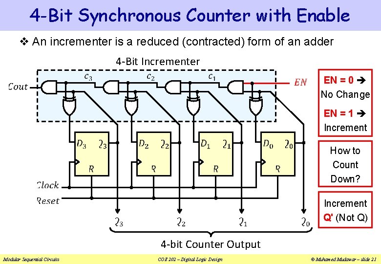
4 -Bit Synchronous Counter with Enable v An incrementer is a reduced (contracted) form of an adder 4 -Bit Incrementer EN = 0 No Change EN = 1 Increment How to Count Down? Increment Q' (Not Q) 4 -bit Counter Output Modular Sequential Circuits COE 202 – Digital Logic Design © Muhamed Mudawar – slide 21

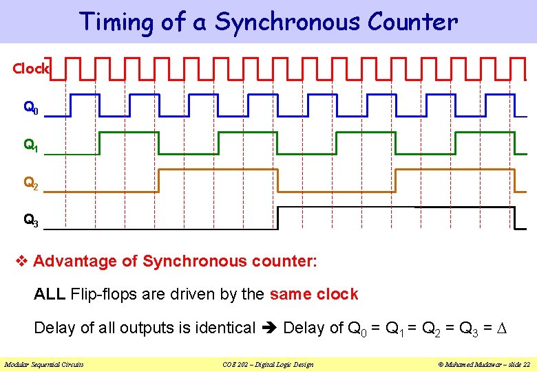
Timing of a Synchronous Counter Clock Q 0 Q 1 Q 2 Q 3 v Advantage of Synchronous counter: ALL Flip-flops are driven by the same clock Delay of all outputs is identical Delay of Q 0 = Q 1 = Q 2 = Q 3 = Modular Sequential Circuits COE 202 – Digital Logic Design © Muhamed Mudawar – slide 22

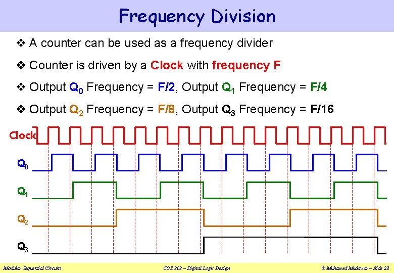
Frequency Division v A counter can be used as a frequency divider v Counter is driven by a Clock with frequency F v Output Q 0 Frequency = F/2, Output Q 1 Frequency = F/4 v Output Q 2 Frequency = F/8, Output Q 3 Frequency = F/16 Clock Q 0 Q 1 Q 2 Q 3 Modular Sequential Circuits COE 202 – Digital Logic Design © Muhamed Mudawar – slide 23

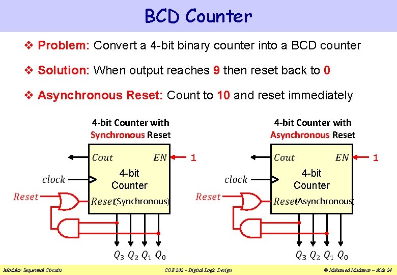
BCD Counter v Problem: Convert a 4 -bit binary counter into a BCD counter v Solution: When output reaches 9 then reset back to 0 v Asynchronous Reset: Count to 10 and reset immediately 4 -bit Counter with Synchronous Reset (Asynchronous) COE 202 – Digital Logic Design 1 4 -bit Counter (Synchronous) Modular Sequential Circuits 1 4 -bit Counter with Asynchronous Reset © Muhamed Mudawar – slide 24

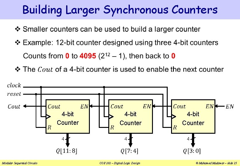
Building Larger Synchronous Counters v 4 -bit Counter 4 Modular Sequential Circuits 4 -bit Counter 4 COE 202 – Digital Logic Design 4 © Muhamed Mudawar – slide 25

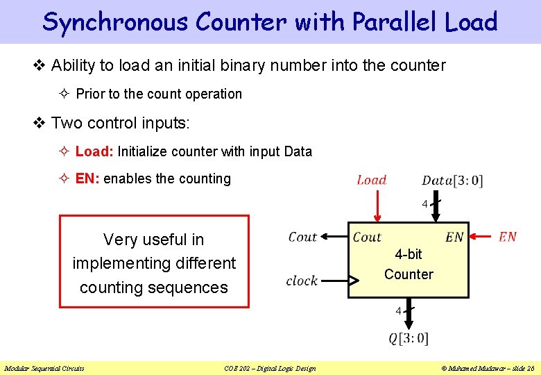
Synchronous Counter with Parallel Load v Ability to load an initial binary number into the counter ² Prior to the count operation v Two control inputs: ² Load: Initialize counter with input Data ² EN: enables the counting 4 Very useful in implementing different counting sequences 4 -bit Counter 4 Modular Sequential Circuits COE 202 – Digital Logic Design © Muhamed Mudawar – slide 26

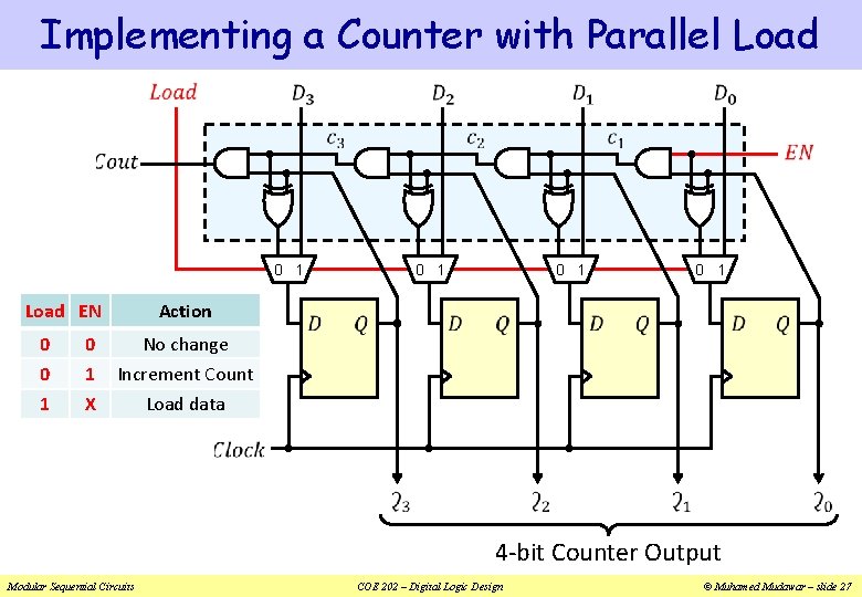
Implementing a Counter with Parallel Load 0 1 Load EN Action 0 0 No change 0 1 Increment Count 1 X Load data 0 1 4 -bit Counter Output Modular Sequential Circuits COE 202 – Digital Logic Design © Muhamed Mudawar – slide 27

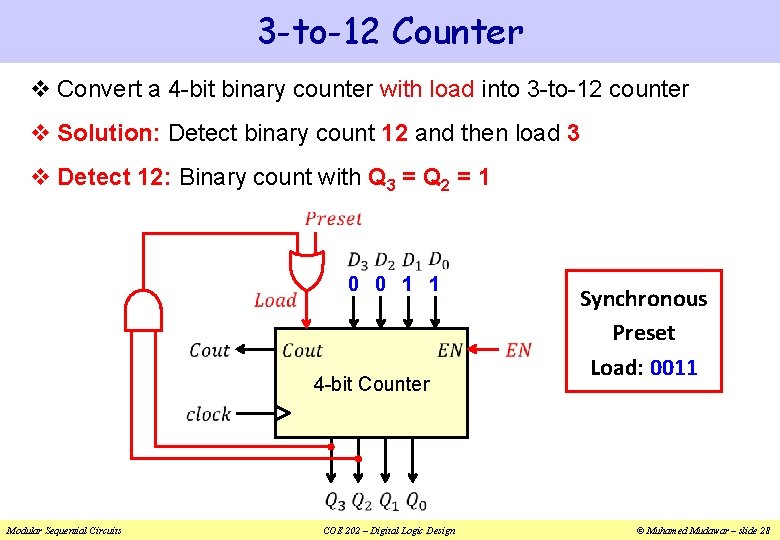
3 -to-12 Counter v Convert a 4 -bit binary counter with load into 3 -to-12 counter v Solution: Detect binary count 12 and then load 3 v Detect 12: Binary count with Q 3 = Q 2 = 1 0 0 1 1 4 -bit Counter Synchronous Preset Load: 0011 Modular Sequential Circuits COE 202 – Digital Logic Design © Muhamed Mudawar – slide 28

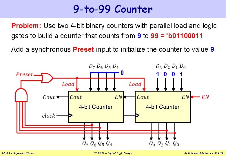
9 -to-99 Counter Problem: Use two 4 -bit binary counters with parallel load and logic gates to build a counter that counts from 9 to 99 = 'b 01100011 Add a synchronous Preset input to initialize the counter to value 9 0 1 0 0 1 4 -bit Counter Modular Sequential Circuits COE 202 – Digital Logic Design © Muhamed Mudawar – slide 29

Memory v Large array or storage cells, capable of storing many 0's and 1's v Random Access Memory: bits can be accessed randomly v Memory is addressable Data_in Memory address consists of k bits Can address 2 k words in memory n Address Each word consists of n bits Read v Memory capacity = 2 k × n bits Write v Two control functions: Read and Write Read: Data_out Memory [Address] k Memory Unit 2 k × n bits n Data_out Write: Memory [Address] Data_in Modular Sequential Circuits COE 202 – Digital Logic Design © Muhamed Mudawar – slide 30

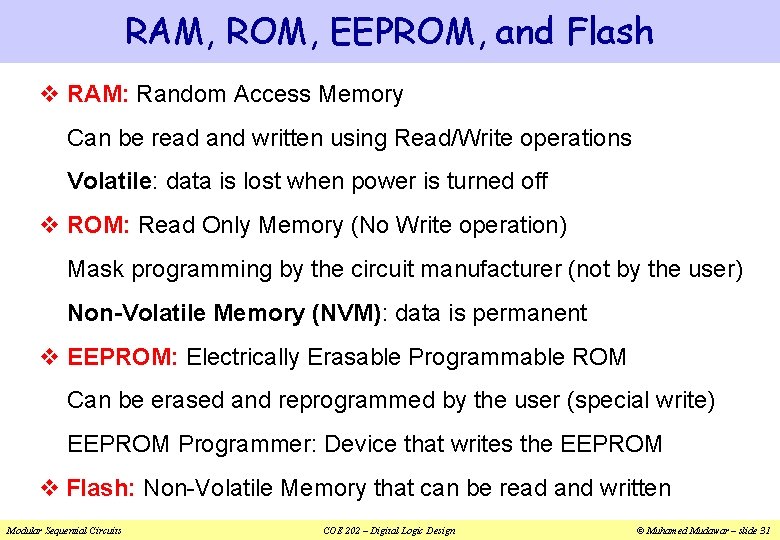
RAM, ROM, EEPROM, and Flash v RAM: Random Access Memory Can be read and written using Read/Write operations Volatile: data is lost when power is turned off v ROM: Read Only Memory (No Write operation) Mask programming by the circuit manufacturer (not by the user) Non-Volatile Memory (NVM): data is permanent v EEPROM: Electrically Erasable Programmable ROM Can be erased and reprogrammed by the user (special write) EEPROM Programmer: Device that writes the EEPROM v Flash: Non-Volatile Memory that can be read and written Modular Sequential Circuits COE 202 – Digital Logic Design © Muhamed Mudawar – slide 31

ROM Memory v Address consists of k bits 2 k memory addresses v At each memory address, there is a word consisting of n bits v The n-bit word appears at the data output of the ROM v ROM does not have data inputs or a write operation Address k ROM 2 k × n bits n Data_out v ROM memory is useful for implementing Boolean Functions v Also useful for storing permanent data Modular Sequential Circuits COE 202 – Digital Logic Design © Muhamed Mudawar – slide 32

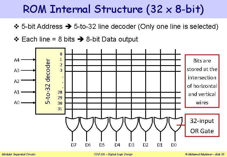
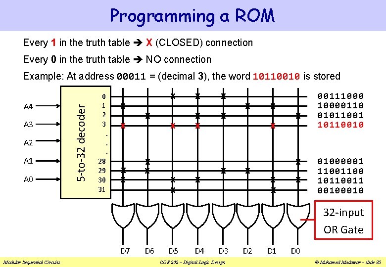
ROM Internal Structure (32 x 8 -bit) v 5 -bit Address 5 -to-32 line decoder (Only one line is selected) A 4 A 3 A 2 A 1 A 0 5 -to-32 decoder v Each line = 8 bits 8 -bit Data output 0 1 2 3 28 29 30 31 Bits are stored at the intersection of horizontal and vertical wires . . . 32 -input OR Gate D 7 Modular Sequential Circuits D 6 D 5 D 4 D 3 COE 202 – Digital Logic Design D 2 D 1 D 0 © Muhamed Mudawar – slide 33

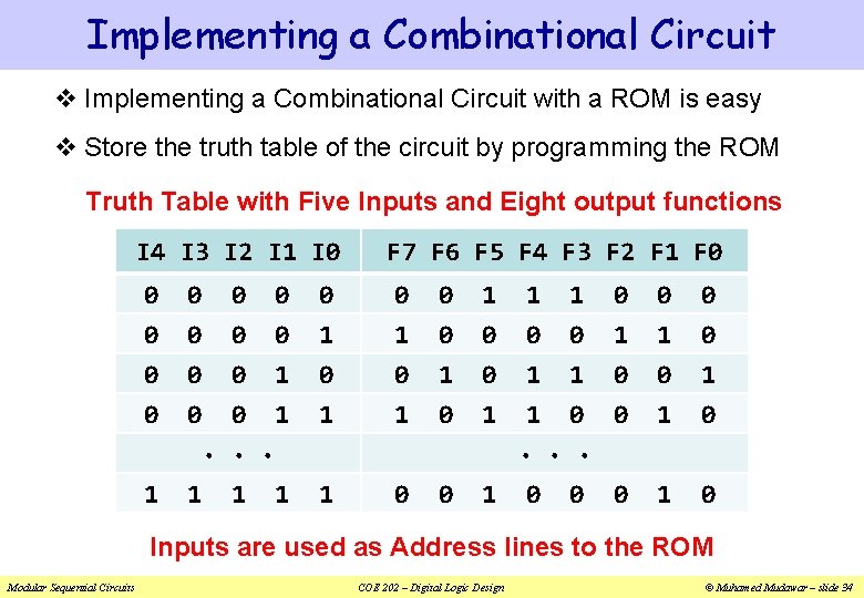
Implementing a Combinational Circuit v Implementing a Combinational Circuit with a ROM is easy v Store the truth table of the circuit by programming the ROM Truth Table with Five Inputs and Eight output functions I 4 I 3 I 2 I 1 I 0 F 7 F 6 F 5 F 4 F 3 F 2 F 1 F 0 0 0 0 0 1 0 0 1 0 0 0 1 · · · 1 1 1 0 0 1 1 0 1 0 0 0 1 1 0 0 · · · 1 0 0 0 1 0 Inputs are used as Address lines to the ROM Modular Sequential Circuits COE 202 – Digital Logic Design © Muhamed Mudawar – slide 34

Programming a ROM Every 1 in the truth table X (CLOSED) connection Every 0 in the truth table NO connection A 4 A 3 A 2 A 1 A 0 5 -to-32 decoder Example: At address 00011 = (decimal 3), the word 10110010 is stored 0 1 2 3 28 29 30 31 x. . . x x x x x x x 001110000110 010110010 01000001 1100 10110011 0010 32 -input OR Gate D 7 Modular Sequential Circuits D 6 D 5 D 4 D 3 COE 202 – Digital Logic Design D 2 D 1 D 0 © Muhamed Mudawar – slide 35

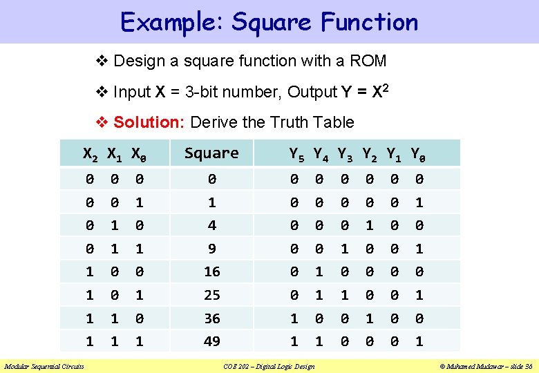
Example: Square Function v Design a square function with a ROM v Input X = 3 -bit number, Output Y = X 2 v Solution: Derive the Truth Table X 2 X 1 X 0 Modular Sequential Circuits Square Y 5 Y 4 Y 3 Y 2 Y 1 Y 0 0 0 0 1 1 0 0 0 1 0 4 0 0 0 1 1 9 0 0 1 1 0 0 16 0 1 0 1 25 0 1 1 0 0 1 1 1 0 36 1 0 0 1 1 1 49 1 1 0 0 0 1 COE 202 – Digital Logic Design © Muhamed Mudawar – slide 36

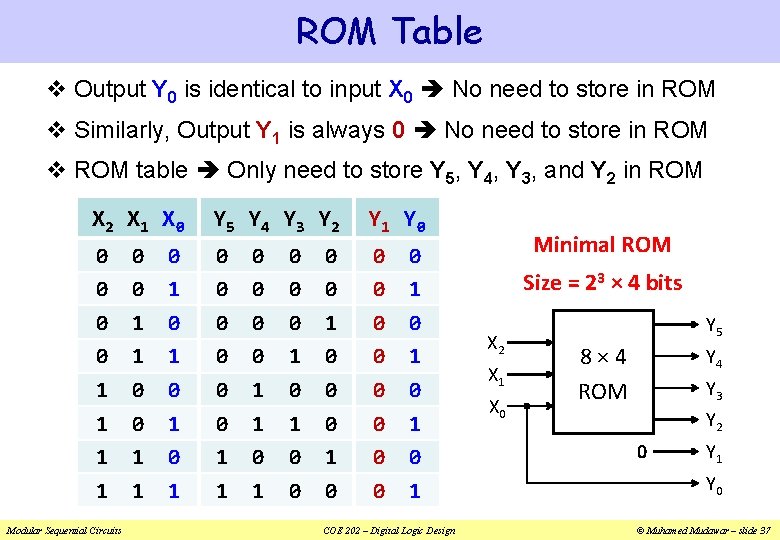
ROM Table v Output Y 0 is identical to input X 0 No need to store in ROM v Similarly, Output Y 1 is always 0 No need to store in ROM v ROM table Only need to store Y 5, Y 4, Y 3, and Y 2 in ROM X 2 X 1 X 0 Y 5 Y 4 Y 3 Y 2 Y 1 Y 0 0 0 1 0 0 0 1 0 0 0 1 1 0 0 0 0 1 0 1 1 0 0 1 0 0 1 1 1 0 0 0 1 Modular Sequential Circuits COE 202 – Digital Logic Design Minimal ROM Size = 23 × 4 bits X 2 X 1 X 0 Y 5 8× 4 ROM Y 4 Y 3 Y 2 0 Y 1 Y 0 © Muhamed Mudawar – slide 37