Introduction to Sequential Circuits COE 202 Digital Logic

- Slides: 28

Introduction to Sequential Circuits COE 202 Digital Logic Design Dr. Muhamed Mudawar King Fahd University of Petroleum and Minerals

Presentation Outline v Introduction to Sequential Circuits v Synchronous versus Asynchronous v Latches v Flip-Flops v Characteristic Tables and Equations Introduction to Sequential Circuits COE 202 – Digital Logic Design © Muhamed Mudawar – slide 2

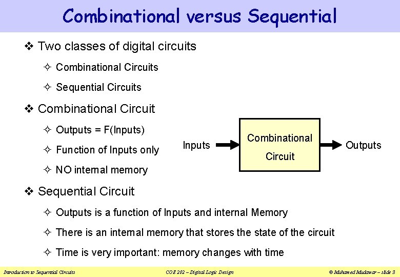
Combinational versus Sequential v Two classes of digital circuits ² Combinational Circuits ² Sequential Circuits v Combinational Circuit ² Outputs = F(Inputs) ² Function of Inputs only Inputs Combinational Outputs Circuit ² NO internal memory v Sequential Circuit ² Outputs is a function of Inputs and internal Memory ² There is an internal memory that stores the state of the circuit ² Time is very important: memory changes with time Introduction to Sequential Circuits COE 202 – Digital Logic Design © Muhamed Mudawar – slide 3

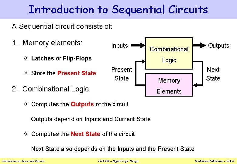
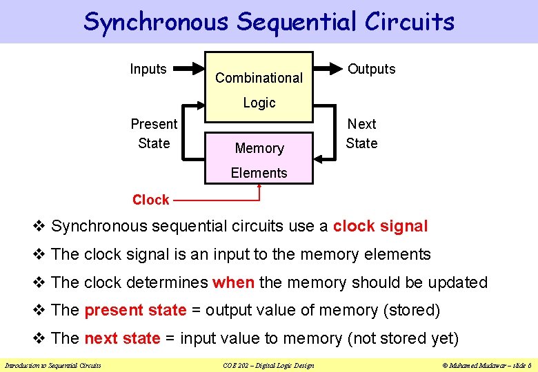
Introduction to Sequential Circuits A Sequential circuit consists of: 1. Memory elements: Inputs Combinational ² Latches or Flip-Flops ² Store the Present State Outputs Logic Present State 2. Combinational Logic Memory Next State Elements ² Computes the Outputs of the circuit Outputs depend on Inputs and Current State ² Computes the Next State of the circuit Next State also depends on the Inputs and the Present State Introduction to Sequential Circuits COE 202 – Digital Logic Design © Muhamed Mudawar – slide 4

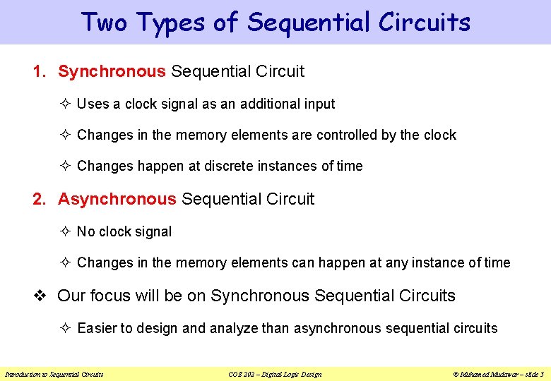
Two Types of Sequential Circuits 1. Synchronous Sequential Circuit ² Uses a clock signal as an additional input ² Changes in the memory elements are controlled by the clock ² Changes happen at discrete instances of time 2. Asynchronous Sequential Circuit ² No clock signal ² Changes in the memory elements can happen at any instance of time v Our focus will be on Synchronous Sequential Circuits ² Easier to design and analyze than asynchronous sequential circuits Introduction to Sequential Circuits COE 202 – Digital Logic Design © Muhamed Mudawar – slide 5

Synchronous Sequential Circuits Inputs Combinational Outputs Logic Present State Memory Next State Elements Clock v Synchronous sequential circuits use a clock signal v The clock signal is an input to the memory elements v The clock determines when the memory should be updated v The present state = output value of memory (stored) v The next state = input value to memory (not stored yet) Introduction to Sequential Circuits COE 202 – Digital Logic Design © Muhamed Mudawar – slide 6

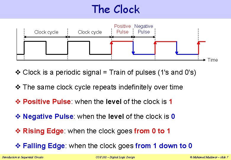
The Clock cycle Positive Negative Pulse Time v Clock is a periodic signal = Train of pulses (1's and 0's) v The same clock cycle repeats indefinitely over time v Positive Pulse: when the level of the clock is 1 v Negative Pulse: when the level of the clock is 0 v Rising Edge: when the clock goes from 0 to 1 v Falling Edge: when the clock goes from 1 down to 0 Introduction to Sequential Circuits COE 202 – Digital Logic Design © Muhamed Mudawar – slide 7

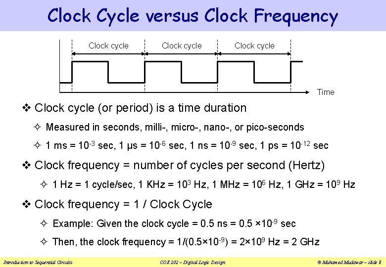
Clock Cycle versus Clock Frequency Clock cycle Time v Clock cycle (or period) is a time duration ² Measured in seconds, milli-, micro-, nano-, or pico-seconds ² 1 ms = 10 -3 sec, 1 µs = 10 -6 sec, 1 ns = 10 -9 sec, 1 ps = 10 -12 sec v Clock frequency = number of cycles per second (Hertz) ² 1 Hz = 1 cycle/sec, 1 KHz = 103 Hz, 1 MHz = 106 Hz, 1 GHz = 109 Hz v Clock frequency = 1 / Clock Cycle ² Example: Given the clock cycle = 0. 5 ns = 0. 5 × 10 -9 sec ² Then, the clock frequency = 1/(0. 5× 10 -9) = 2× 10⁹ Hz = 2 GHz Introduction to Sequential Circuits COE 202 – Digital Logic Design © Muhamed Mudawar – slide 8

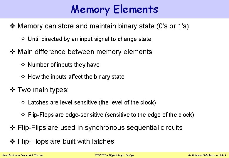
Memory Elements v Memory can store and maintain binary state (0's or 1's) ² Until directed by an input signal to change state v Main difference between memory elements ² Number of inputs they have ² How the inputs affect the binary state v Two main types: ² Latches are level-sensitive (the level of the clock) ² Flip-Flops are edge-sensitive (sensitive to the edge of the clock) v Flip-Flips are used in synchronous sequential circuits v Flip-Flops are built with latches Introduction to Sequential Circuits COE 202 – Digital Logic Design © Muhamed Mudawar – slide 9

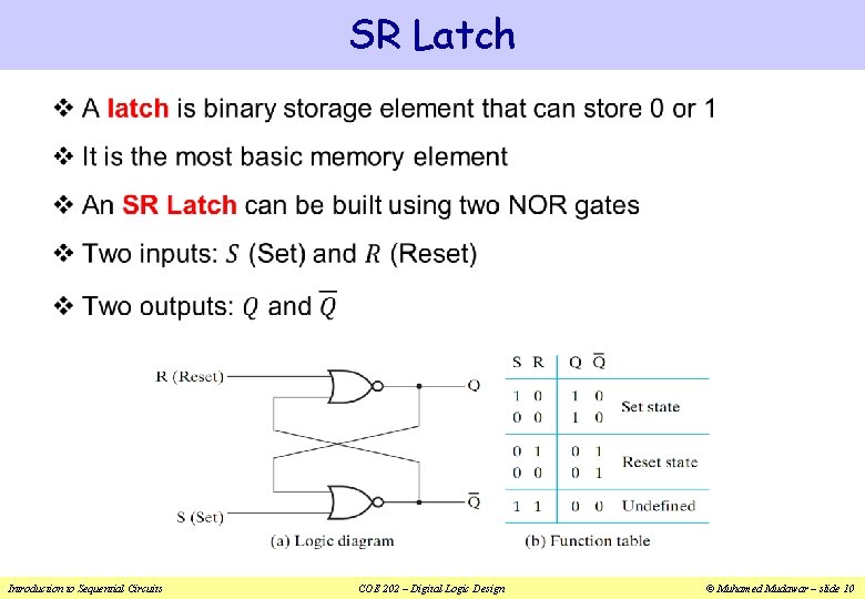
SR Latch v Introduction to Sequential Circuits COE 202 – Digital Logic Design © Muhamed Mudawar – slide 10

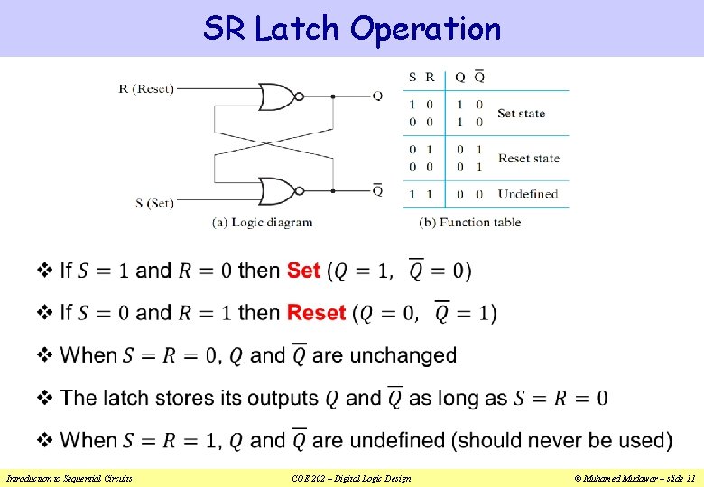
SR Latch Operation v Introduction to Sequential Circuits COE 202 – Digital Logic Design © Muhamed Mudawar – slide 11

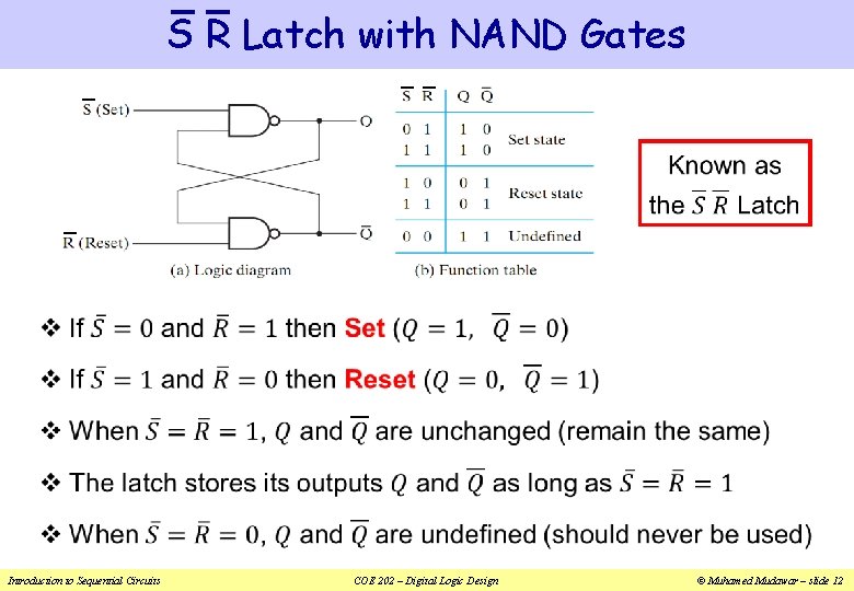
S R Latch with NAND Gates v Introduction to Sequential Circuits COE 202 – Digital Logic Design © Muhamed Mudawar – slide 12

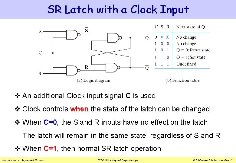
SR Latch with a Clock Input S R v An additional Clock input signal C is used v Clock controls when the state of the latch can be changed v When C=0, the S and R inputs have no effect on the latch The latch will remain in the same state, regardless of S and R v When C=1, then normal SR latch operation Introduction to Sequential Circuits COE 202 – Digital Logic Design © Muhamed Mudawar – slide 13

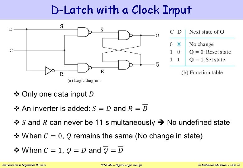
D-Latch with a Clock Input S R v Introduction to Sequential Circuits COE 202 – Digital Logic Design © Muhamed Mudawar – slide 14

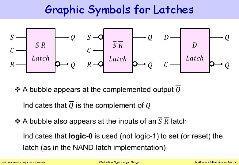
Graphic Symbols for Latches v Introduction to Sequential Circuits COE 202 – Digital Logic Design © Muhamed Mudawar – slide 15

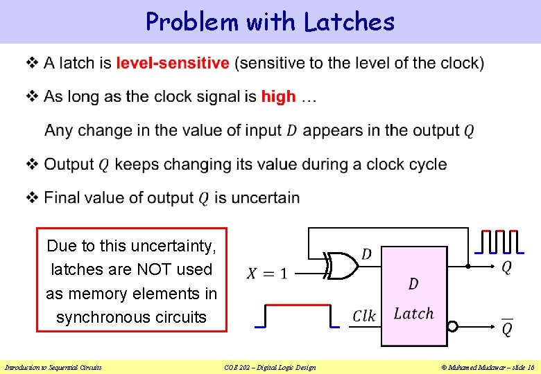
Problem with Latches v Due to this uncertainty, latches are NOT used as memory elements in synchronous circuits Introduction to Sequential Circuits COE 202 – Digital Logic Design © Muhamed Mudawar – slide 16

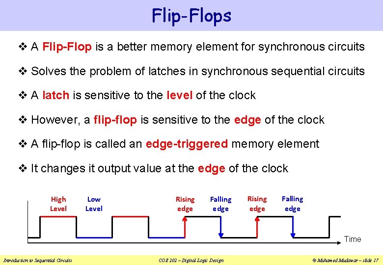
Flip-Flops v A Flip-Flop is a better memory element for synchronous circuits v Solves the problem of latches in synchronous sequential circuits v A latch is sensitive to the level of the clock v However, a flip-flop is sensitive to the edge of the clock v A flip-flop is called an edge-triggered memory element v It changes it output value at the edge of the clock High Level Low Level Rising edge Falling edge Time Introduction to Sequential Circuits COE 202 – Digital Logic Design © Muhamed Mudawar – slide 17

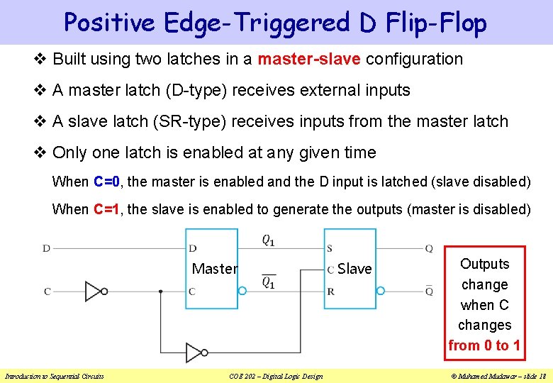
Positive Edge-Triggered D Flip-Flop v Built using two latches in a master-slave configuration v A master latch (D-type) receives external inputs v A slave latch (SR-type) receives inputs from the master latch v Only one latch is enabled at any given time When C=0, the master is enabled and the D input is latched (slave disabled) When C=1, the slave is enabled to generate the outputs (master is disabled) Master Introduction to Sequential Circuits COE 202 – Digital Logic Design Slave Outputs change when C changes from 0 to 1 © Muhamed Mudawar – slide 18

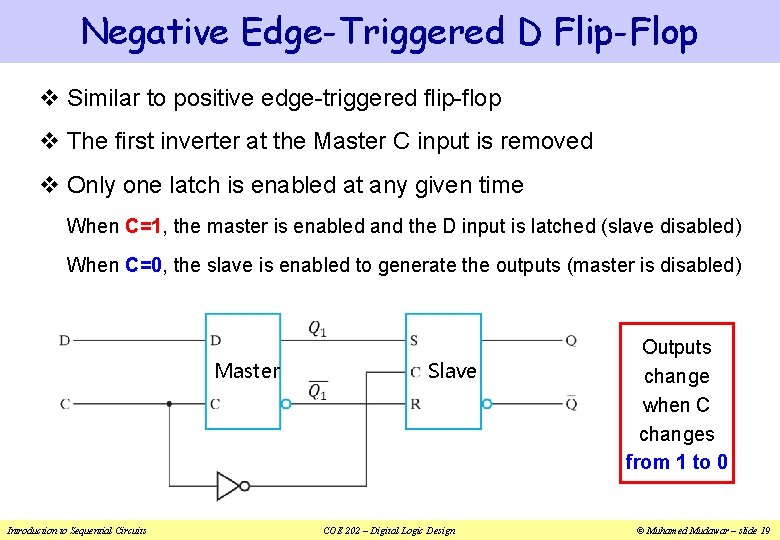
Negative Edge-Triggered D Flip-Flop v Similar to positive edge-triggered flip-flop v The first inverter at the Master C input is removed v Only one latch is enabled at any given time When C=1, the master is enabled and the D input is latched (slave disabled) When C=0, the slave is enabled to generate the outputs (master is disabled) Master Introduction to Sequential Circuits Slave COE 202 – Digital Logic Design Outputs change when C changes from 1 to 0 © Muhamed Mudawar – slide 19

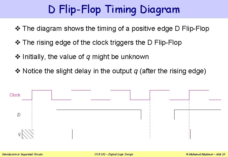
D Flip-Flop Timing Diagram v The diagram shows the timing of a positive edge D Flip-Flop v The rising edge of the clock triggers the D Flip-Flop v Initially, the value of q might be unknown v Notice the slight delay in the output q (after the rising edge) Introduction to Sequential Circuits COE 202 – Digital Logic Design © Muhamed Mudawar – slide 20

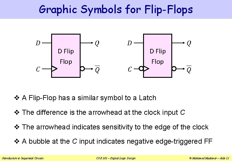
Graphic Symbols for Flip-Flops D Flip Flop v A Flip-Flop has a similar symbol to a Latch v The difference is the arrowhead at the clock input C v The arrowhead indicates sensitivity to the edge of the clock v A bubble at the C input indicates negative edge-triggered FF Introduction to Sequential Circuits COE 202 – Digital Logic Design © Muhamed Mudawar – slide 21

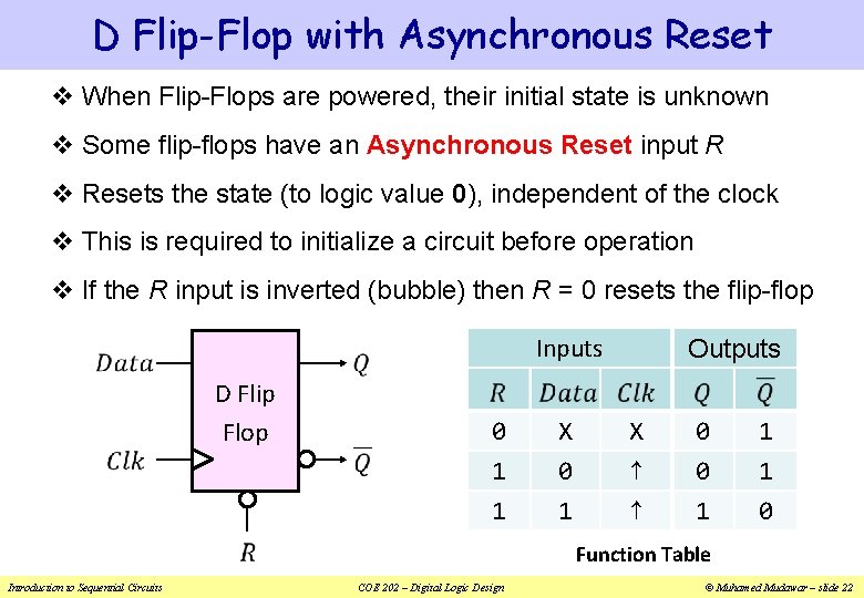
D Flip-Flop with Asynchronous Reset v When Flip-Flops are powered, their initial state is unknown v Some flip-flops have an Asynchronous Reset input R v Resets the state (to logic value 0), independent of the clock v This is required to initialize a circuit before operation v If the R input is inverted (bubble) then R = 0 resets the flip-flop Inputs D Flip Flop 0 1 X 0 X ↑ 0 0 1 1 ↑ 1 0 Introduction to Sequential Circuits Outputs Function Table COE 202 – Digital Logic Design © Muhamed Mudawar – slide 22

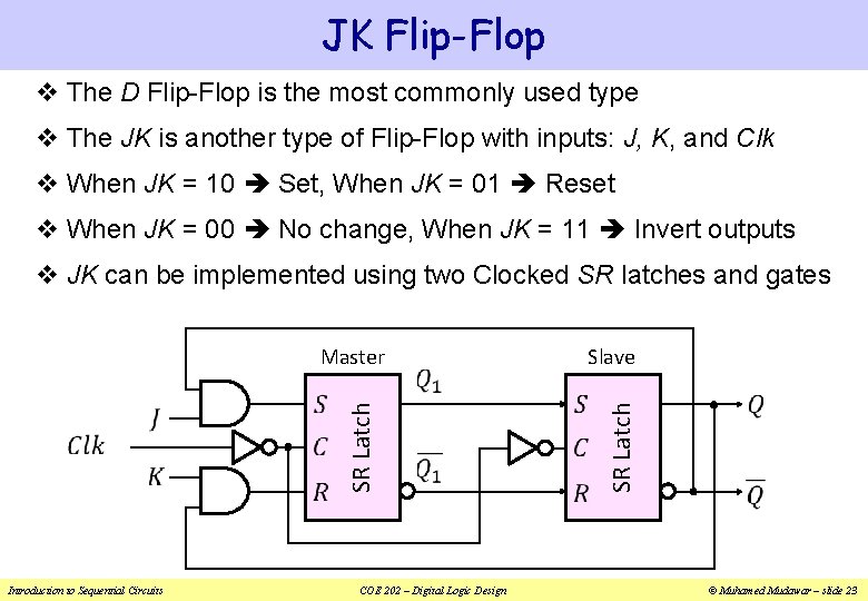
JK Flip-Flop v The D Flip-Flop is the most commonly used type v The JK is another type of Flip-Flop with inputs: J, K, and Clk v When JK = 10 Set, When JK = 01 Reset v When JK = 00 No change, When JK = 11 Invert outputs v JK can be implemented using two Clocked SR latches and gates Introduction to Sequential Circuits Slave COE 202 – Digital Logic Design SR Latch Master © Muhamed Mudawar – slide 23

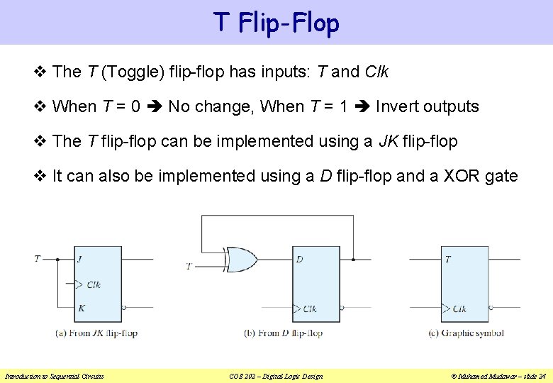
T Flip-Flop v The T (Toggle) flip-flop has inputs: T and Clk v When T = 0 No change, When T = 1 Invert outputs v The T flip-flop can be implemented using a JK flip-flop v It can also be implemented using a D flip-flop and a XOR gate Introduction to Sequential Circuits COE 202 – Digital Logic Design © Muhamed Mudawar – slide 24

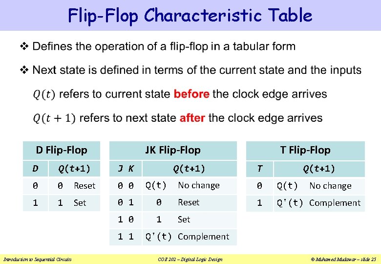
Flip-Flop Characteristic Table v JK Flip-Flop D Flip-Flop J K Q(t+1) D Q(t+1) 0 0 Reset 0 0 Q(t) 1 1 Set 0 1 1 Introduction to Sequential Circuits T Flip-Flop T Q(t+1) No change 0 Q(t) 0 Reset 1 Q'(t) Complement 1 Set No change Q'(t) Complement COE 202 – Digital Logic Design © Muhamed Mudawar – slide 25

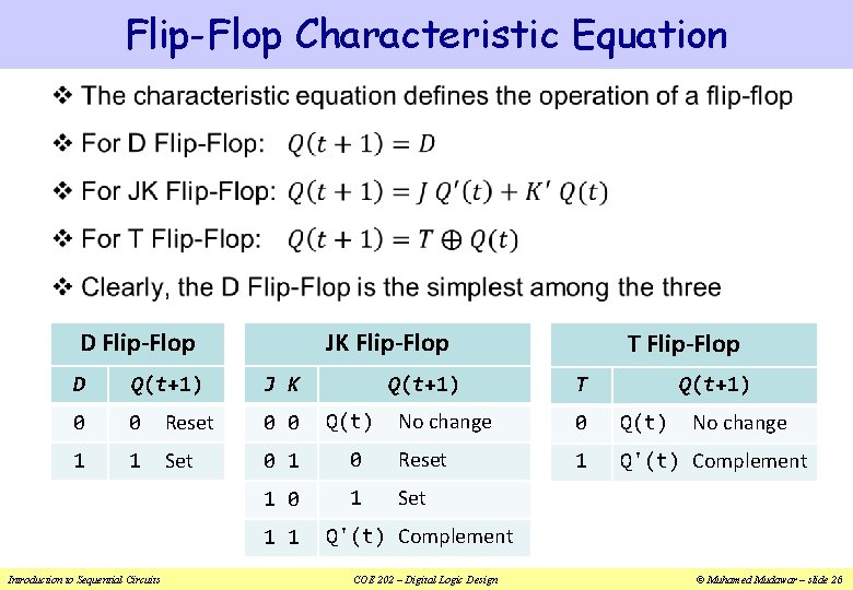
Flip-Flop Characteristic Equation v JK Flip-Flop D Flip-Flop J K Q(t+1) D Q(t+1) 0 0 Reset 0 0 Q(t) 1 1 Set 0 1 1 Introduction to Sequential Circuits T Flip-Flop T Q(t+1) No change 0 Q(t) 0 Reset 1 Q'(t) Complement 1 Set No change Q'(t) Complement COE 202 – Digital Logic Design © Muhamed Mudawar – slide 26

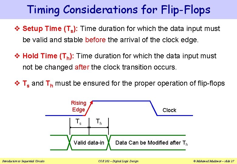
Timing Considerations for Flip-Flops v Setup Time (Ts): Time duration for which the data input must be valid and stable before the arrival of the clock edge. v Hold Time (Th): Time duration for which the data input must not be changed after the clock transition occurs. v Ts and Th must be ensured for the properation of flip-flops Rising Edge Ts Clock Th Valid data-in Introduction to Sequential Circuits Data Can be Modified after Th COE 202 – Digital Logic Design © Muhamed Mudawar – slide 27

Summary v In a sequential circuit there is internal memory ² Output is a function of current inputs and present state ² The stored memory value defines the present state ² Similarly, the next state depends on current inputs and present state v Two types of sequential circuits: ² Synchronous sequential circuits are clocked (easier to implement) ² Asynchronous sequential circuits are not clocked v Two types of Memory elements: Latches and Flip-Flops v Latches are level-sensitive, flip-flops are edge-triggered v Flip-flops are better memory elements for synchronous circuits v A flip-flop is described using a characteristic table and equation Introduction to Sequential Circuits COE 202 – Digital Logic Design © Muhamed Mudawar – slide 28