Sequential Logic z Sequential Circuits y Simple circuits
![Shift Register Verilog module shift_reg (out, in, clk); output [4: 1] out; input in, Shift Register Verilog module shift_reg (out, in, clk); output [4: 1] out; input in,](https://slidetodoc.com/presentation_image/0d8ea45725fcd250c534e3d41f9c8790/image-32.jpg)
- Slides: 40

Sequential Logic z Sequential Circuits y Simple circuits with feedback y Latches y Edge-triggered flip-flops z Timing Methodologies y Cascading flip-flops for properation y Clock skew z Basic Registers y Shift registers y Counters CS 150 - Spring 2007 – Lec. #5 – Sequential Logic - 1

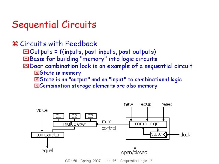
Sequential Circuits z Circuits with Feedback y Outputs = f(inputs, past outputs) y Basis for building "memory" into logic circuits y Door combination lock is an example of a sequential circuit x. State is memory x. State is an "output" and an "input" to combinational logic x. Combination storage elements are also memory new equal reset value C 1 C 2 multiplexer C 3 mux control comb. logic state comparator equal open/closed CS 150 - Spring 2007 – Lec. #5 – Sequential Logic - 2 clock

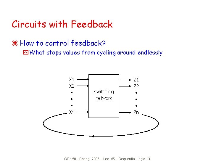
Circuits with Feedback z How to control feedback? y What stops values from cycling around endlessly X 1 X 2 • • • Xn switching network Z 1 Z 2 • • • Zn CS 150 - Spring 2007 – Lec. #5 – Sequential Logic - 3

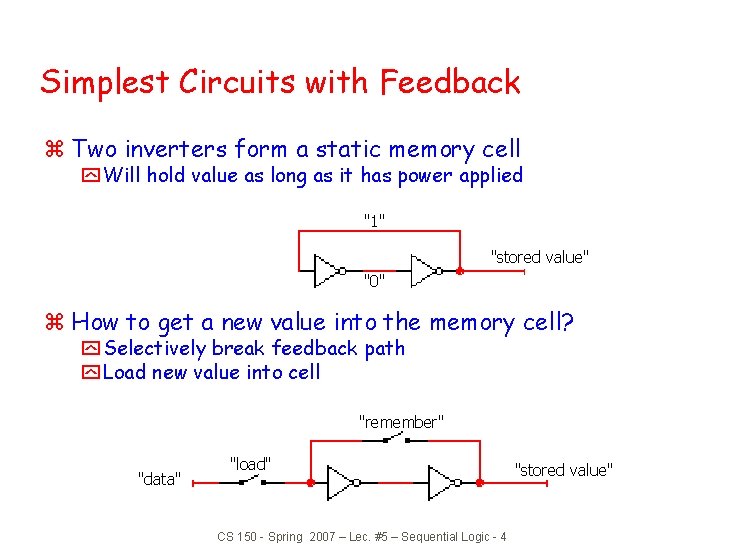
Simplest Circuits with Feedback z Two inverters form a static memory cell y Will hold value as long as it has power applied "1" "stored value" "0" z How to get a new value into the memory cell? y Selectively break feedback path y Load new value into cell "remember" "data" "load" CS 150 - Spring 2007 – Lec. #5 – Sequential Logic - 4 "stored value"

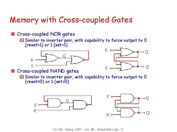
Memory with Cross-coupled Gates z Cross-coupled NOR gates y Similar to inverter pair, with capability to force output to 0 (reset=1) or 1 (set=1) R Q S Q' Q R S z Cross-coupled NAND gates y Similar to inverter pair, with capability to force output to 0 (reset=0) or 1 (set=0) S' R' Q S' R' CS 150 - Spring 2007 – Lec. #5 – Sequential Logic - 5 Q Q'

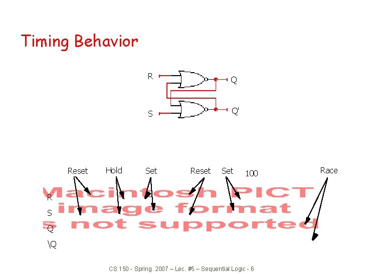
Timing Behavior Reset Hold R Q S Q' Set Reset Set 100 R S Q Q CS 150 - Spring 2007 – Lec. #5 – Sequential Logic - 6 Race

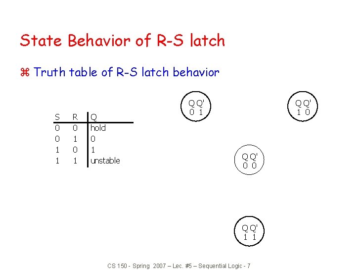
State Behavior of R-S latch z Truth table of R-S latch behavior S 0 0 1 1 R 0 1 Q hold 0 1 unstable Q Q' 0 1 Q Q' 1 0 Q Q' 0 0 Q Q' 1 1 CS 150 - Spring 2007 – Lec. #5 – Sequential Logic - 7

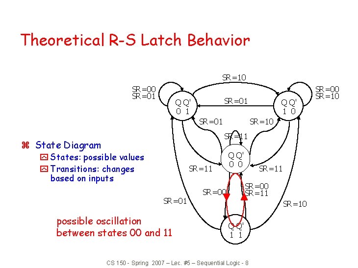
Theoretical R-S Latch Behavior SR=10 SR=01 Q Q' 0 1 SR=01 Q Q' 1 0 SR=11 z State Diagram y States: possible values y Transitions: changes based on inputs SR=11 SR=01 possible oscillation between states 00 and 11 Q Q' 0 0 SR=11 SR=00 SR=10 Q Q' 1 1 CS 150 - Spring 2007 – Lec. #5 – Sequential Logic - 8 SR=00 SR=10

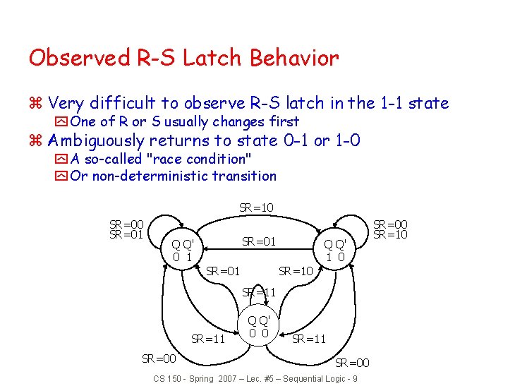
Observed R-S Latch Behavior z Very difficult to observe R-S latch in the 1 -1 state y One of R or S usually changes first z Ambiguously returns to state 0 -1 or 1 -0 y A so-called "race condition" y Or non-deterministic transition SR=10 SR=01 Q Q' 0 1 SR=01 Q Q' 1 0 SR=11 SR=00 Q Q' 0 0 SR=11 SR=00 CS 150 - Spring 2007 – Lec. #5 – Sequential Logic - 9 SR=00 SR=10

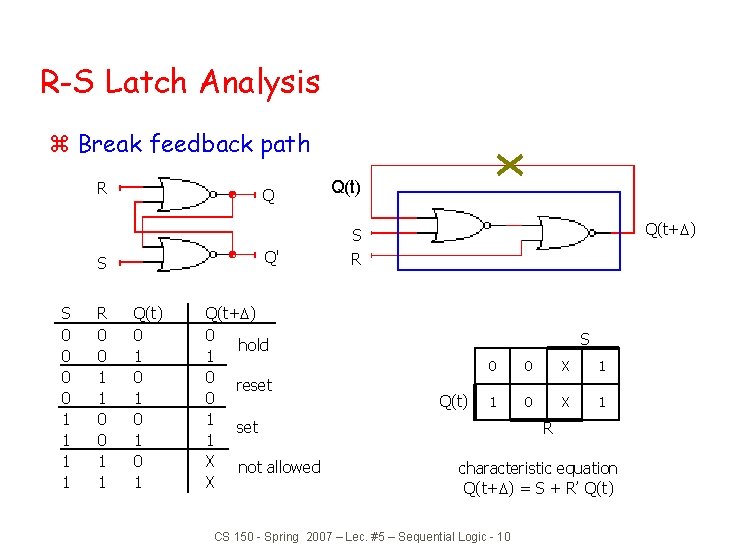
R-S Latch Analysis z Break feedback path R Q Q(t) Q(t+ ) S Q' S S 0 0 1 1 R 0 0 1 1 Q(t) 0 1 0 1 Q(t+ ) 0 hold 1 0 reset 0 1 set 1 X not allowed X R S Q(t) 0 0 X 1 1 0 X 1 R characteristic equation Q(t+ ) = S + R’ Q(t) CS 150 - Spring 2007 – Lec. #5 – Sequential Logic - 10

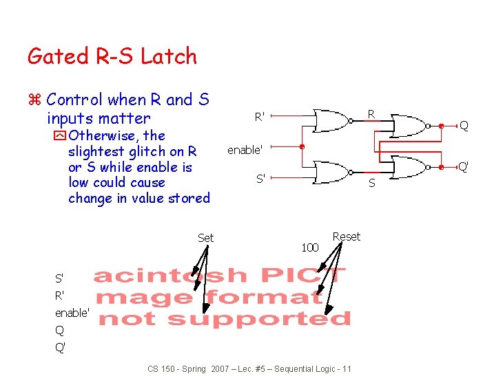
Gated R-S Latch z Control when R and S inputs matter y Otherwise, the slightest glitch on R or S while enable is low could cause change in value stored Set R R' Q enable' Q' S' S 100 Reset S' R' enable' Q Q' CS 150 - Spring 2007 – Lec. #5 – Sequential Logic - 11

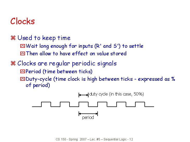
Clocks z Used to keep time y Wait long enough for inputs (R' and S') to settle y Then allow to have effect on value stored z Clocks are regular periodic signals y Period (time between ticks) y Duty-cycle (time clock is high between ticks - expressed as % of period) duty cycle (in this case, 50%) period CS 150 - Spring 2007 – Lec. #5 – Sequential Logic - 12

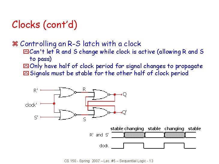
Clocks (cont’d) z Controlling an R-S latch with a clock y Can't let R and S change while clock is active (allowing R and S to pass) y Only have half of clock period for signal changes to propagate y Signals must be stable for the other half of clock period R' R Q clock' S' Q' S stable changing stable R' and S' clock CS 150 - Spring 2007 – Lec. #5 – Sequential Logic - 13

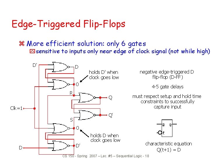
Edge-Triggered Flip-Flops z More efficient solution: only 6 gates y sensitive to inputs only near edge of clock signal (not while high) D’ D holds D' when clock goes low negative edge-triggered D flip-flop (D-FF) 0 R 4 -5 gate delays Q Clk=1 must respect setup and hold time constraints to successfully capture input Q’ S 0 holds D when clock goes low D D’ characteristic equation Q(t+1) = D CS 150 - Spring 2007 – Lec. #5 – Sequential Logic - 18

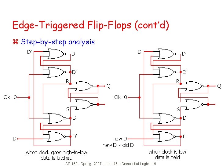
Edge-Triggered Flip-Flops (cont’d) z Step-by-step analysis D’ D’ D D D’ R Q Clk=0 S S D D Q D’ when clock goes high-to-low data is latched D D’ new D old D when clock is low data is held CS 150 - Spring 2007 – Lec. #5 – Sequential Logic - 19

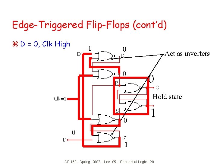
Edge-Triggered Flip-Flops (cont’d) z D = 0, Clk High D’ 1 0 D’ 0 R 0 Q Hold state Clk=1 S D 0 0 D Act as inverters D 1 D’ 1 CS 150 - Spring 2007 – Lec. #5 – Sequential Logic - 20

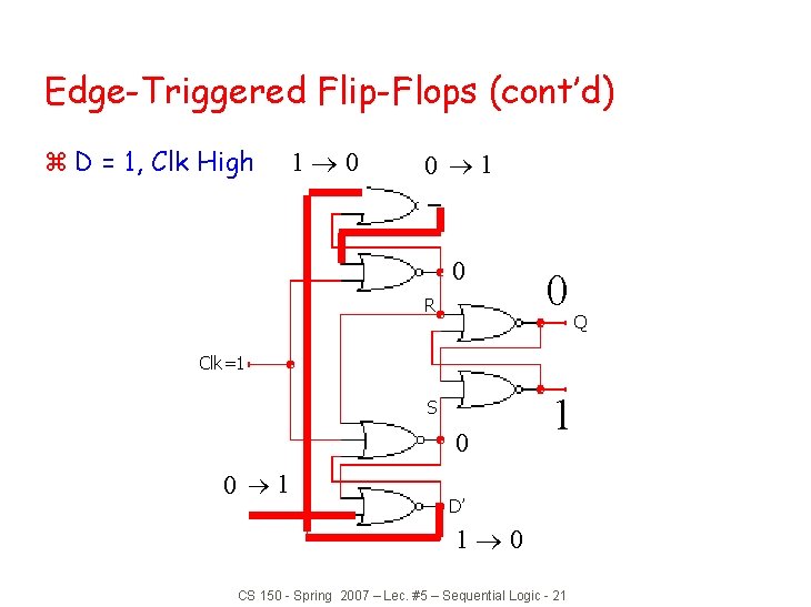
Edge-Triggered Flip-Flops (cont’d) z D = 1, Clk High 11 ® 0 0® 1 D’ D D’ 0 R 0 Clk=1 S D 0 0 ® 01 D 1 D’ 1® 0 CS 150 - Spring 2007 – Lec. #5 – Sequential Logic - 21 Q

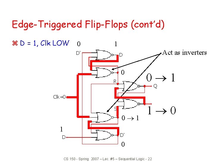
Edge-Triggered Flip-Flops (cont’d) z D = 1, Clk LOW 0 01 D’ Act as inverters D D’ 0 0® 1 R Q Clk=0 S D 0 1 0 D ® 1 1® 0 D’ 0 CS 150 - Spring 2007 – Lec. #5 – Sequential Logic - 22

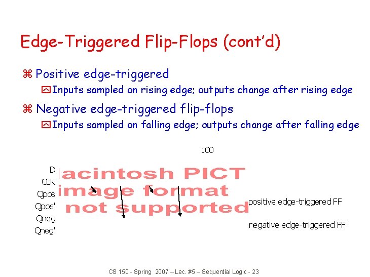
Edge-Triggered Flip-Flops (cont’d) z Positive edge-triggered y Inputs sampled on rising edge; outputs change after rising edge z Negative edge-triggered flip-flops y Inputs sampled on falling edge; outputs change after falling edge 100 D CLK Qpos' Qneg' positive edge-triggered FF negative edge-triggered FF CS 150 - Spring 2007 – Lec. #5 – Sequential Logic - 23

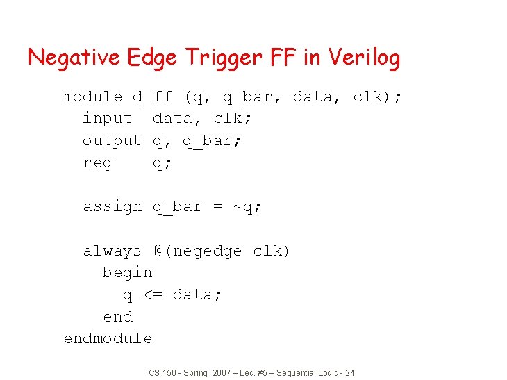
Negative Edge Trigger FF in Verilog module d_ff (q, q_bar, data, clk); input data, clk; output q, q_bar; reg q; assign q_bar = ~q; always @(negedge clk) begin q <= data; endmodule CS 150 - Spring 2007 – Lec. #5 – Sequential Logic - 24

Announcements z Cancel Lab Section Tu 11 -2 PM starting next week y Young assigned to Th 5 -8 PM lab y Allen assigned to W 5 -8 PM lab (3 TAs!) z Homework #2 Bug y Problem 7(b) revised and posted to the web z Starting Thursday, lecture meets in 159 Mulford CS 150 - Spring 2007 – Lec. #5 – Sequential Logic - 25

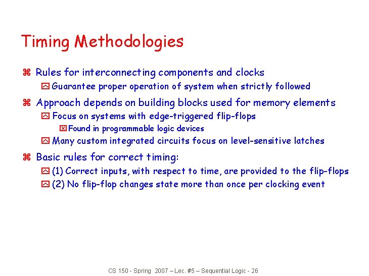
Timing Methodologies z Rules for interconnecting components and clocks y Guarantee properation of system when strictly followed z Approach depends on building blocks used for memory elements y Focus on systems with edge-triggered flip-flops x Found in programmable logic devices y Many custom integrated circuits focus on level-sensitive latches z Basic rules for correct timing: y (1) Correct inputs, with respect to time, are provided to the flip-flops y (2) No flip-flop changes state more than once per clocking event CS 150 - Spring 2007 – Lec. #5 – Sequential Logic - 26

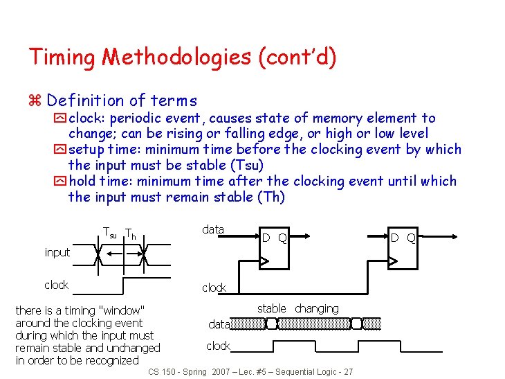
Timing Methodologies (cont’d) z Definition of terms y clock: periodic event, causes state of memory element to change; can be rising or falling edge, or high or low level y setup time: minimum time before the clocking event by which the input must be stable (Tsu) y hold time: minimum time after the clocking event until which the input must remain stable (Th) data Tsu Th D Q input clock there is a timing "window" around the clocking event during which the input must remain stable and unchanged in order to be recognized stable changing data clock CS 150 - Spring 2007 – Lec. #5 – Sequential Logic - 27 D Q

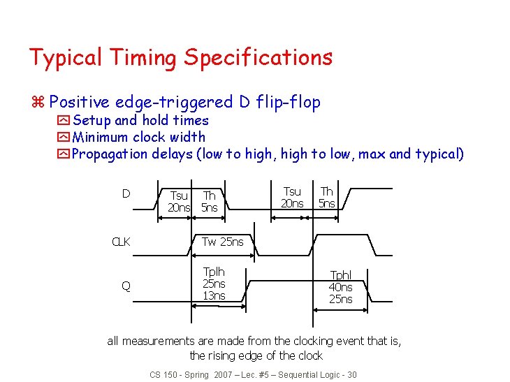
Typical Timing Specifications z Positive edge-triggered D flip-flop y Setup and hold times y Minimum clock width y Propagation delays (low to high, high to low, max and typical) D CLK Q Tsu Th 20 ns 5 ns Tsu 20 ns Th 5 ns Tw 25 ns Tplh 25 ns 13 ns Tphl 40 ns 25 ns all measurements are made from the clocking event that is, the rising edge of the clock CS 150 - Spring 2007 – Lec. #5 – Sequential Logic - 30

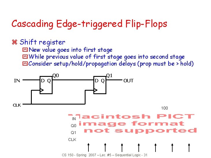
Cascading Edge-triggered Flip-Flops z Shift register y New value goes into first stage y While previous value of first stage goes into second stage y Consider setup/hold/propagation delays (prop must be > hold) IN D Q Q 0 D Q Q 1 OUT CLK 100 IN Q 0 Q 1 CLK CS 150 - Spring 2007 – Lec. #5 – Sequential Logic - 31

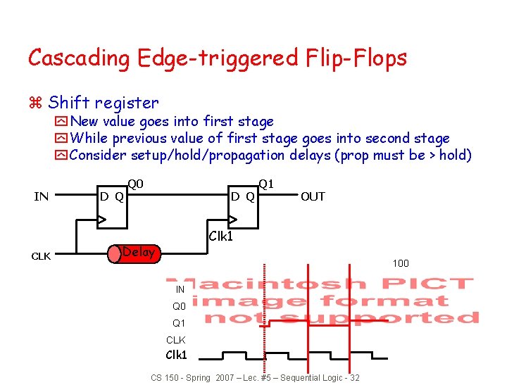
Cascading Edge-triggered Flip-Flops z Shift register y New value goes into first stage y While previous value of first stage goes into second stage y Consider setup/hold/propagation delays (prop must be > hold) IN CLK D Q Q 0 D Q Q 1 OUT Clk 1 Delay 100 IN Q 0 Q 1 CLK Clk 1 CS 150 - Spring 2007 – Lec. #5 – Sequential Logic - 32

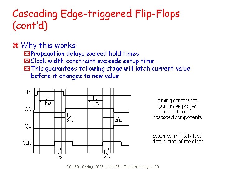
Cascading Edge-triggered Flip-Flops (cont’d) z Why this works y Propagation delays exceed hold times y Clock width constraint exceeds setup time y This guarantees following stage will latch current value before it changes to new value In Tsu 4 ns Q 0 Tp 3 ns timing constraints guarantee properation of cascaded components Q 1 assumes infinitely fast distribution of the clock CLK Th 2 ns CS 150 - Spring 2007 – Lec. #5 – Sequential Logic - 33

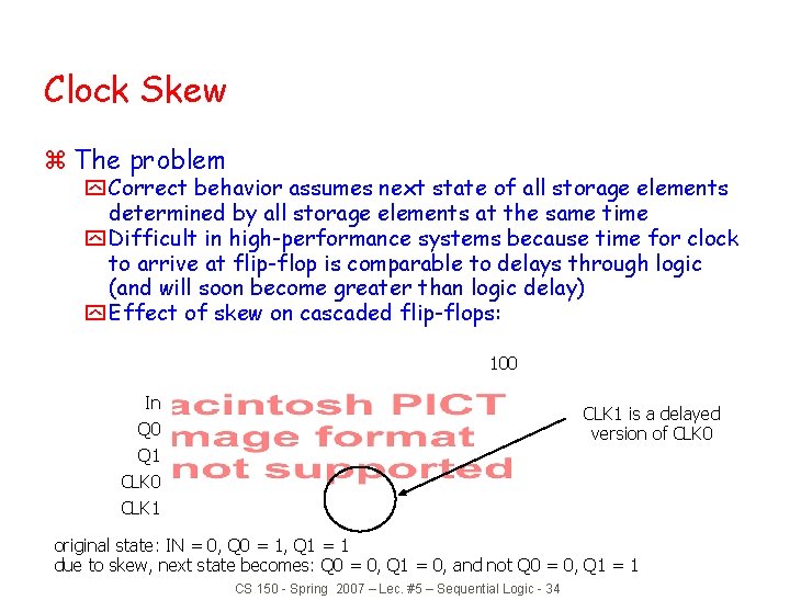
Clock Skew z The problem y Correct behavior assumes next state of all storage elements determined by all storage elements at the same time y Difficult in high-performance systems because time for clock to arrive at flip-flop is comparable to delays through logic (and will soon become greater than logic delay) y Effect of skew on cascaded flip-flops: 100 In Q 0 Q 1 CLK 0 CLK 1 is a delayed version of CLK 0 original state: IN = 0, Q 0 = 1, Q 1 = 1 due to skew, next state becomes: Q 0 = 0, Q 1 = 0, and not Q 0 = 0, Q 1 = 1 CS 150 - Spring 2007 – Lec. #5 – Sequential Logic - 34

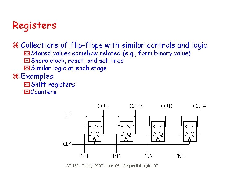
Registers z Collections of flip-flops with similar controls and logic y Stored values somehow related (e. g. , form binary value) y Share clock, reset, and set lines y Similar logic at each stage z Examples y Shift registers y Counters OUT 1 OUT 2 OUT 3 OUT 4 "0" R S R S D Q D Q CLK IN 1 IN 2 IN 3 CS 150 - Spring 2007 – Lec. #5 – Sequential Logic - 37 IN 4

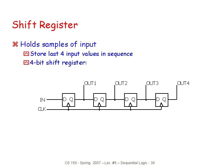
Shift Register z Holds samples of input y Store last 4 input values in sequence y 4 -bit shift register: OUT 1 IN D Q OUT 2 OUT 3 D Q CLK CS 150 - Spring 2007 – Lec. #5 – Sequential Logic - 38 D Q OUT 4

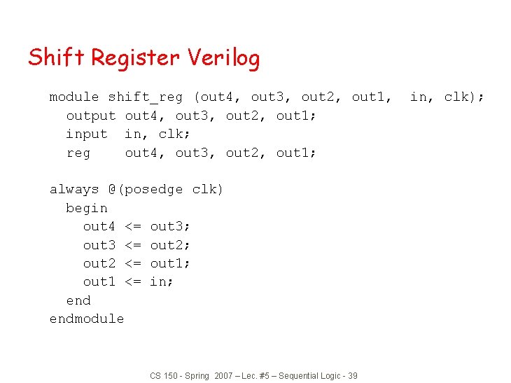
Shift Register Verilog module shift_reg (out 4, out 3, out 2, out 1, output out 4, out 3, out 2, out 1; input in, clk; reg out 4, out 3, out 2, out 1; always @(posedge clk) begin out 4 <= out 3; out 3 <= out 2; out 2 <= out 1; out 1 <= in; endmodule CS 150 - Spring 2007 – Lec. #5 – Sequential Logic - 39 in, clk);
![Shift Register Verilog module shiftreg out in clk output 4 1 out input in Shift Register Verilog module shift_reg (out, in, clk); output [4: 1] out; input in,](https://slidetodoc.com/presentation_image/0d8ea45725fcd250c534e3d41f9c8790/image-32.jpg)
Shift Register Verilog module shift_reg (out, in, clk); output [4: 1] out; input in, clk; reg [4: 1] out; always @(posedge clk) begin out <= {out[3: 1], in}; endmodule CS 150 - Spring 2007 – Lec. #5 – Sequential Logic - 40

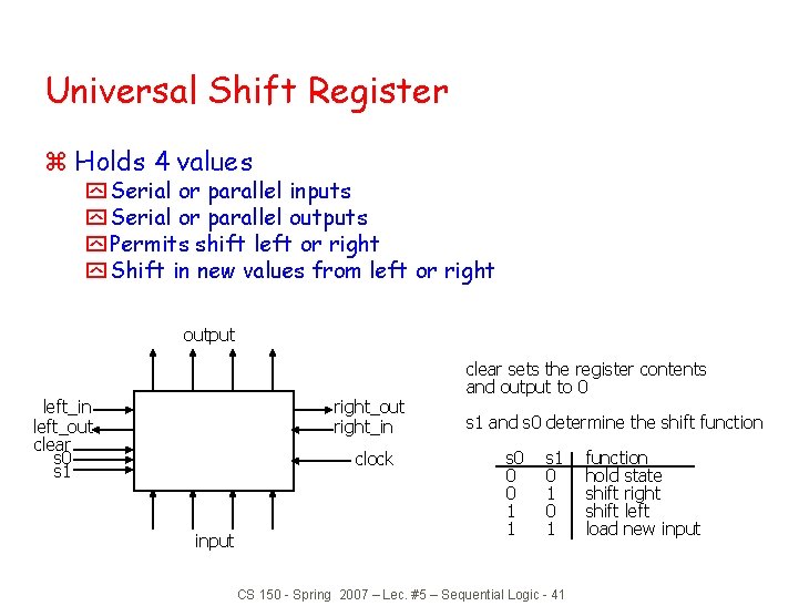
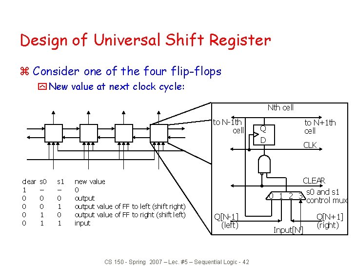
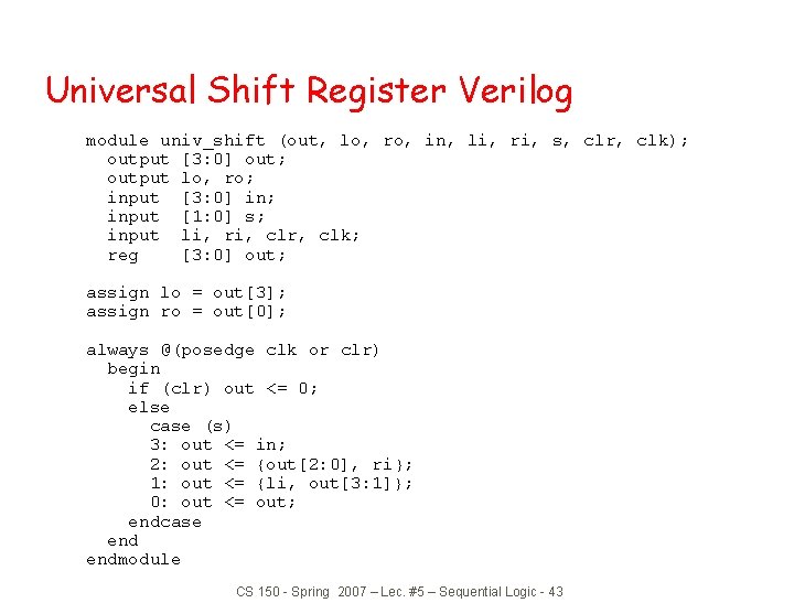
Universal Shift Register z Holds 4 values y Serial or parallel inputs y Serial or parallel outputs y Permits shift left or right y Shift in new values from left or right output left_in left_out clear s 0 s 1 right_out right_in clock input clear sets the register contents and output to 0 s 1 and s 0 determine the shift function s 0 0 0 1 1 s 1 0 1 CS 150 - Spring 2007 – Lec. #5 – Sequential Logic - 41 function hold state shift right shift left load new input

Design of Universal Shift Register z Consider one of the four flip-flops y New value at next clock cycle: Nth cell to N-1 th cell clear 1 0 0 s 0 – 0 0 1 1 s 1 – 0 1 new value 0 output value of FF to left (shift right) output value of FF to right (shift left) input to N+1 th cell Q D CLK CLEAR 0 1 2 3 s 0 and s 1 control mux Q[N-1] (left) CS 150 - Spring 2007 – Lec. #5 – Sequential Logic - 42 Input[N] Q[N+1] (right)

Universal Shift Register Verilog module univ_shift (out, lo, ro, in, li, ri, s, clr, clk); output [3: 0] out; output lo, ro; input [3: 0] in; input [1: 0] s; input li, ri, clr, clk; reg [3: 0] out; assign lo = out[3]; assign ro = out[0]; always @(posedge clk or clr) begin if (clr) out <= 0; else case (s) 3: out <= in; 2: out <= {out[2: 0], ri}; 1: out <= {li, out[3: 1]}; 0: out <= out; endcase endmodule CS 150 - Spring 2007 – Lec. #5 – Sequential Logic - 43

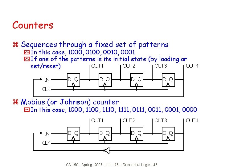
Counters z Sequences through a fixed set of patterns y In this case, 1000, 0100, 0010, 0001 y If one of the patterns is its initial state (by loading or OUT 1 OUT 2 OUT 3 OUT 4 set/reset) IN D Q D Q CLK z Mobius (or Johnson) counter y In this case, 1000, 1110, 1111, 0011, 0000 OUT 1 IN D Q OUT 2 OUT 3 D Q CLK CS 150 - Spring 2007 – Lec. #5 – Sequential Logic - 46 D Q OUT 4

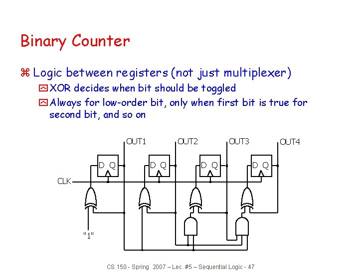
Binary Counter z Logic between registers (not just multiplexer) y XOR decides when bit should be toggled y Always for low-order bit, only when first bit is true for second bit, and so on OUT 1 D Q OUT 2 D Q OUT 3 D Q OUT 4 D Q CLK "1" CS 150 - Spring 2007 – Lec. #5 – Sequential Logic - 47

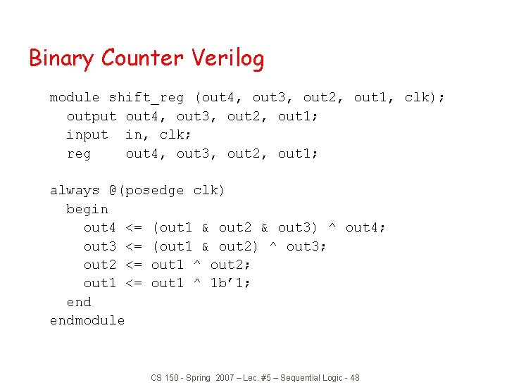
Binary Counter Verilog module shift_reg (out 4, out 3, out 2, out 1, clk); output out 4, out 3, out 2, out 1; input in, clk; reg out 4, out 3, out 2, out 1; always @(posedge clk) begin out 4 <= (out 1 & out 2 & out 3) ^ out 4; out 3 <= (out 1 & out 2) ^ out 3; out 2 <= out 1 ^ out 2; out 1 <= out 1 ^ 1 b’ 1; endmodule CS 150 - Spring 2007 – Lec. #5 – Sequential Logic - 48

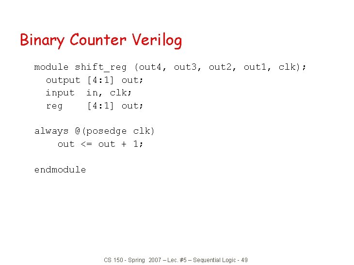
Binary Counter Verilog module shift_reg (out 4, out 3, out 2, out 1, clk); output [4: 1] out; input in, clk; reg [4: 1] out; always @(posedge clk) out <= out + 1; endmodule CS 150 - Spring 2007 – Lec. #5 – Sequential Logic - 49

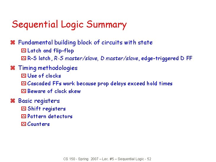
Sequential Logic Summary z Fundamental building block of circuits with state y Latch and flip-flop y R-S latch, R-S master/slave, D master/slave, edge-triggered D FF z Timing methodologies y Use of clocks y Cascaded FFs work because prop delays exceed hold times y Beware of clock skew z Basic registers y Shift registers y Pattern detectors y Counters CS 150 - Spring 2007 – Lec. #5 – Sequential Logic - 52