impractical things endure and retain their vitality for


 –socker ball Cage diameter - 0. 71 nm Optical")
 Carbyne – linear polymer chain of C atoms Young")


 - multi-scale material: cells -> spirals -> threads ->")


: Two steps to become a metal, First hint to")


 ARPES result:")


 J. P. Pouget et al. (1976) T>Tc – \"Diffuse")


")


2 PF 6 at 10 K in its SP")
2 X TCO TSP Thermal behavior of a S=1/2 Heisenberg chain")


4 Br 0. 3 H 2 O, blue bronze K 0. 3")

: metallic 2 electrons in a period transition")


 to experimental I-V curve (Ogawa, Miyano, S. B.")

- Slides: 59
“impractical things endure and retain their vitality for thousands of years, whereas necessary, practical things survive only briefly” Kasimir Malevich, manifesto of Suprematism Serguei Brazovskii CNRS & University Paris-Sud, Orsay, France Physics of cooperative electronic states in low-dimensional systems.
Lecture 1. Low dimensional electronic systems: organic crystals, chain- and layered compounds, interfaces, conducting polymers. Symmetry broken ground states: charge- spin- and bond density waves; Wigner crystal; charge ordering; electronic ferroelectricity; Mott, Peierls and excitonic insulators. Lecture 2. Excitations and carriers in correlated electronic systems: excitons, polarons, solitons, phasons. Lecture 3. Electronic ferroelectricity: from realities of organic conductors to perspectives of conjugated polymers. The related physics of solitons and domain walls. Lecture 4. Theory elements for correlated electronic systems in one and two dimensions. Lecture 5. Dynamical phase transitions in cooperative electronic systems induced by fast optical pumping or voltage pulses. Lecture 6. Story of field-induced rising of the superconductivity or distraction of the insulating state. Transformations of collective electronic states under the electric field or the current.
« In the beginning was the Word, … and without him was not anything made that was made » Physical Review 1964 & Scientific American 1965 W. A. Little , Stanford University POSSIBILITY OF A SYNTHESIZING AN ORGANIC SUPERCONDUCTOR. SUPERCONDUCTIVITY AT ROOM TEMPERATURE. It has not yet been achieved, but … it is possible to synthesize organic materials that … conduct electricity without resistance. Little drawing: conjugated polymer the polyene backbone with ligands R Superconductivity: Tc ~ ħωph exp(-1/λ) λ –coupling of electrons to vibrations with a frequency ωph~1/ M 1/2
New directions of material science initiated by the quest for HTSC: Inorganic world of d-electrons Ø Inorganic chains/planes like MX 3/MX 2 (M=Nb, Ta, Ti, Mo; X=S, Se, Te), Pt chain compounds, surface structures of adsorbed atoms The carbon world of pi-conjugated systems: Ø Organic conducting crystals Ø Molecular crystals with a charge transfer Ø Conjugated polymers Ø Graphite (intercolated) Ø Fullerenes (pen&Sun born), nano-tubes, graphene New states or their new realizations found in search for HTSC: conductors, superconductors, magnetics, ferroelectrics, charge ordered states, charge/spin density waves and their special versions in high magnetic fields, optically and electronically active polymers
Ready or promising for applications: Polymers for Light Emitting or Harvesting Organic Ferroelectrics As. F 6 Sb. F 6 Re. O 4 PF 6 New targets: Optical, Voltage, and STM switching in layered electronic crystals (Ta. S 2) Ljubljana-Slovenia, POSTECH, U. of Tokyo
Synthetic metals first contributors Inorganic chain Quasi 1 D – 2 D Charge and Spin density waves T. Sambongi, R. Comes, P. Monceau Conducting polymers Quasi 1 D A. J. Heeger, A. Mac. Diarmid H. Shirakawa, Y. W. Park, R. Friend Nanotubes big bang since 1993 Sumio Iijima, D. S. Bethune Organic Crystals Superconductivity D. Jérome, K. Bechgaard. (quasi 1 D) E. Yagubskii et al, T. Ishiguro, H. Saito, K. Murata et al (quasi-2 D) Fullerenes 1985 Smalley, Curl & Kroto
All Dimensionalities from Carbon • • • 0 D quantum dots – C 60 1 D quantum wires – carbon nanotubes 1 D polymeric chains 2 D layer - graphene 2 D layered material - graphite 3 D wide gap semicond. - diamond 7
Zero dimensional: Fullerene (C 60) –socker ball Cage diameter - 0. 71 nm Optical gap – 1. 9 V Crystalline undoped Fullerene fcc structure 8
One dimensional: Carbon nanotubes (CNT) Carbyne – linear polymer chain of C atoms Young modulus Diamond 1. 22 103 Gpa CNT 103 GPa Carbyne 5 104 GPa (40 times of diamond) Multi-wall 1991 Single-wall 1993 CNT can be a very good conductor, thin (1 nm) and resistant 1 nm 9
Two dimensional - graphene Basic block – benzene ring 10
Layered = quasi-2 D graphite: Pristine semi-metal; Reversible intercalation: electrode in Lithium-ion bataries Intercolated conductor, up to superconductivity as C 6 S 3 D form: the diamond 11
Q. Where such versiality comes from? A. Hybridization of the orbitals. Q. Why do we need the hybridization? A. It diminishes the kinetic energy (ΔxΔp~� ) Q. What does it mean the hybridization? A. See next slides. 12
Carbon: Hybridized Orbitals There are four valence electrons. In the ground state valence is 2 (rem. CO). But electron can easy come from 2 s 2 to 2 p 2, now the valence is 4 (rem. CO 2). 2 p 2 2 s 2 1 s 2 The 2 s and 2 p wave functions can mix forming hybridized orbitals. 13
and bonds • Two side-to-side 2 p orbitals form a bond. • Two co-axial 2 p orbitals form the bond. 14
Three possible types of mixing I. SP hybridization Carbyne – linear polymer 15
II. SP 2 hybridization Graphite SP 2 16
III. SP 3 hybridization Diamond 17
Saturated polymers – traditional plastics SP 3 H H H C C H Polyethylene (CH 2)x – saturated polymer with all saturated bonds, all electrons form the chain sceleton C H H Conjugated polymers: linear chains, phenyl based, etc SP 2 18
Heeger, Mac. Diarmid and Shirakawa Nobel Prize in chemistry 2000 « for the discovery and development of electrically conducting polymers » . Inside these noodles: poly-crystals of trans-(CH)x Made conducting under a heavy doping (Y. W. Park)
Helicoidal polyacethelene (K. Akagi, Kyoto) - multi-scale material: cells -> spirals -> threads -> crystalline fibers -> polymer chains -> -electrons -> Peierls-dimerization -> solitons -> confinement
Substituted polyacetylenes - Today’s great variety: chemistry is centered in Kyoto, Hong Kong, Beijing, Semiconductor, excitons, light emission, even Lasing ! 22
Unique conjugated polymes: polyacetylene Dream: the metal Reality: narrow gap insulator H H C C C H H C C H Peierls effect - one dimentional chain of equidistant atoms is unstable with respect to the dimerisation: Spontaneus symmetry braking results in the dielectric state, the gap is open E E Wexp(- -k. F F -k. F 23
Cyclobutane C 4 H 4 4 carbon atoms – 4 π-electrons Instability Jahn-Teller --> Peierls square --> rectangle Wave functions: Half filled doubly degenerate level 2, 3 Ψ 1=cos 0 • n=cnst Ψ 2=cos(πn/2) gain electronic energy -2 D loose deformation energy Similar story in doped Fullerenes Ψ 3=sin(πn/2) Ψ 4=cos πn=(-1)n 24
Isolated benzene ring H C H CH C H Degenerate level is completely filled – no gain from reducing the hexagon symmetry. We only loose the deformation energy N=8 – again the instability, like for N=4: what is next, and at large N ? 25
Peierls model - deformable lattice Main interactions : electron – phonon coupling (electron-electron repulsions are small) Ground state: W = Wel + Wlat W - 0 0 symmetry -
Doped polyacetylene (Y. W. Park): Two steps to become a metal, First hint to existence of solitons conductivity s and magnetic susceptibility χ The major puzzle: spins appear at much higher doping than the metallic conductivity: the whole interval of conduction by spinless – unlike electrons – particles. That and many other propertiese showing up in NMR, ESR, optics have brought the solitons to the sight of experiments 27
Organic crystalline conductors in Japan. Highest current activity in the world. Wide geography: Sapporo, Tohoku, Tokyo, Okayama, Okazaki, Osaka, Kyoto, + Tokyo area alone (and incomplete !): NMR methods in Gakushuin (T. Takahashi) and Tokyo (K. Kanoda) Univ. , Phase diagram experiment and theory (U. of Tokyo – S. Kagoshima, RIKEN – H. Seo) Ferroelectricity (U. Tokyo and RIKEN – Y. Tokura gr. , Kashiwa – H. Okamoto) Unique properties in high magnetic fields – T. Osada, ISSP, Kashiwa Leading edge ultrafast optics – H. Okamoto - Kashiwa, S. Iwai - Tohoku Applied R&D: R. Kato at RIKEN, Yamomoto @ Okazaki, Y. Furukawa at Waseda U. , + much more
The organic conductor TTF-TCNQ k. F F. Zwick et al, PRL (1998) ARPES result: conventional Quasi-1 D material with two open Fermi surfaces originated by two stacks. But other data: TTF at least is the strongest correlated conductor of the whole family.
STM on TTF-TCNQ, Z. -Z. Wang, France TTF+ TCNQ- at T = 63 K – no modulation CDW at 35. 6 K
S. Kagoshima et al. (1976) J. P. Pouget et al. (1976) T>Tc – "Diffuse X-ray scattering" measures local structural correlation without the long range order, T<Tc – bright Bragg spots will appear only below Tc. Lines are in the inter-chain direction: no dependence on K - no correlation among chains. 2 Kf appear at lower T but condense into true Braggs. 4 Kf lines exist since the RT but never condense, 4 Kf CDW = Wigner crystal ever coexists with both metallic and CDW phases.
Charge Transfer Change at High Pressure D. Jerome 1: 3 commensurability locking and its consequences. Collective nature of on-chain transport versus single-particle nature of inter-chain transport On-chain conductivity drops at the 3: 1 lock-in Inter-chain conductivity does not feel the lock-in
Message from/to another world: incommensurate CDWs. Key word - sliding vs pinning. Collective nature of the on-chain conduction in TTF-TCNQ is seen from the nonlinear I-V which are setup below Tc for the 2 Kf CDW
Schematic illustration of liquid and crystal states of charged colloidal dispersion. particle charge of typically 100 e to 1000 e. As the particle concentration increases, the fluid changes into a body-centered cubic crystal and eventually a face-centered cubic crystal Microscopic realizations: Electrons trapped near the liquid He surface, Charge ordering in organic crystals
Q. Can we have the electronic crystal with one electron per unit cell? A. Yes: there are the Wigner Crystals in dilute regime of heterojunction Charge ordering in the dense regime of organic metals Fermi liquid : electron possess a momentum p~p. F , totally delocalized. Wigner crystal: periodic arrangement of almost localized electrons. Need Coulomb repulsion ~e 2/r to dominate over the kinetic energy ~ћ 2/mr 2, Hence r>RB, electron density n<C/RBd Odds against: a strongly quantum crystal – very light electrons rather than heavy atoms - strong zero-point fluctuations around the local positions - easy melting - small C~10 -2
In D=1, Wigner crystallization is allowed even at high density - upon the metallic background – provided e 2/ћv. F>1 It is clearly observed as the “ 4 KF anomaly” (Pouget et al, Kagoshima) Wigner crystal period (one electron per cell) is ½ of that for the CDW, hence the wave number is doubled.
Coulomb Interaction to Cause 4 k. F CDW 2 electrons in a period 2 k. F CDW Coulomb, on-site or long-range 2 /4 k. F CDW The electrons have a strong correlation in their motion because of the repulsive Coulomb interaction. 4 k. F CDW is the introduction to physics of strongly correlated electrons. How common is the charge ordering – Wigner Crystal? Can it be unlocked from the underlying lattice ? -An important issue in today's science of nano-wires.
The world of -electrons: conducting organic crystals. Interplay of common structural instabilities (Peierls insulator) with effects of strong Coulomb interactions (Mott insulator) and nevertheless the superconductivity. (TMTSF)2 PF 6 -(BEDT-TTF)2 Cu[N(CN)2]Br
The world of organic conductors is dominated by e-e repulsion with lattice deformations upon them conterion = dopant X Molecule TMTTF or TMTSF (TMTCF)2 X , C=T, Se ; X=Cl. O 4, BF 4, PF 6, SCN, etc Origin of conducting Fermi-sea: Complete charge transfer between the chain X and the molecular stack; one fermion per two molecules, ¼ filled band – prone to a commensurability effects 42
The ever richest phase diagram of electronic phases. H CO – Charge Ordering + Ferroelectricity AFM – Anti-Ferro. Magnetism SDW – Spin Density Wave SP – Spin-Peierls SC – Superconductivity H axes – field-induced density waves, quantum Hall, oscillating cascades
Low T states on top of the Mott insulator. 1. Spin exchange Jnm. Sn. Sm with J~t 2/U antiferromagnetic state 2. Lattice modulation of J – non-magnetic (singlet) spin-Peierls state AF 2 k. F SDW SP Spin-Peierls r=1 (1 electron per site) Mott-Hubbard localization case of Cu. Ge. O 3 2 k. F bond « CDW » (BOW) r=1/2 (1 electron per dimer) Case of (TMTTF)2 X
X-ray diffuse scattering pattern from (TMTTF)2 PF 6 at 10 K in its SP ground state: weak (1/2, ? ) superlattice spots inside the circles.
Spin susceptibility measurements: (TMTTF)2 X TCO TSP Thermal behavior of a S=1/2 Heisenberg chain J~400 K (Dumm et al PRB 62, 6510 (2000)) no effect at TCO: spin – charge decoupling
Materials on the verge of the Mott transition P ~ 200 bar P ~ 20 kbar anomalous metal T (K) (V 1 -x. Crx)2 O 3 param. insulator param. metal param. insulator AFM insulator Mc. Wham et al. , PRB 7, 1920 (’ 73) Limelette et al. , Science 302, 89 (‘ 03) Georges et al. , J. Phys. 114, 165 (’ 04) (P 0, T 0) TMI metal -(ET)2 Cu[N(CN)2]Cl TN AFM insulator T* superconductor Kino, Fukuyama, JPSJ 65, 2158 (’ 96) Kanoda, Hyperfine Int. 104, 235 (’ 97) Lefebvre et al. , PRL 85, 5420 (’ 00) Limelette et al. , PRL 91, 016401 (‘ 03) Fournier et al. , PRL 90, 127002 (‘ 03) Kagawa et al. , Nature 436, 534 (’ 05)
New intra-molecular charge transfer: Kobayashi family et al. Internal spill-over between overlapping bands originated by two weakly split molecular orbitals. Undoped Four-Layered Two-Gap High-Tc Superconductor. Ba 2 Ca 3 Cu 4 O 8 F 2 Shen group, PRL 07 “Undoped cuprate a 60 K superconductor, apical fluorine, inner and outer Cu. O 2 layers, Fermi surface has large n- and p-doped sheets with the superconducting gap on the n sheet twice that on the p sheet. ” n, p~15%
Phtalocyanine – a borderline of worlds of and d electrons. Its stacks can be both conducting because of -electrons of the ring, and magnetically active because of the transition metal core. These crystals show a metal – insulator transition due to formation of an electronic crystal – a CDW. Its breakdown due to the spin polarization in a high magnetic field gives rise to periodic lattices of solitons.
New attention to ill-conducting organic crystals: Ferromagnetism and Ferroelectricity Studied by various approaches: Electric - Y. Tokura Optics - S. Koshihara , H. Okamoto NMR - K. Kanoda
Inorganic world 1. pi-elctrons – semiconductors, oxygen, chalcogenides 2. d-electrons – transition metals
P-electrons The array of Indium chains at Si 111 surface. Ground state: 2 -fold commensurate CDW, Peierls gap 160 me. V, Tc~120 K. Han Woong Yeom, IBS @ Pos. Tech Conducting and superconducting inorganic polymer (SN)x
K 2 Pt(CN)4 Br 0. 3 H 2 O, blue bronze K 0. 3 Mo. O 3 MX 3 chain conductors: Nb. Se 3, Ta. S 3, etc Tanda lab @ Hokkido
Incommensurate, 3 D ordered Charge Density Waves - CDW ARPES gives electrons’ spectral density, hence E(k) with the gap Δ formed by the CDW Scanning Tunneling Microscopy STM shows the CDW modulation in atomic displacements and the electronic density. Brun, Wang, Monceau, SB CDW wave fronts chains
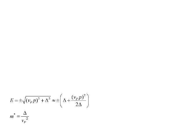
Peierls Instability and Charge Density Waves (CDW): metallic 2 electrons in a period transition in 1 -D insulating The wave length is not related to the original cell size possibility for the incommensurate CDW - ICDW Energy profile as function of the complex order parameter
Collective motion of electronic crystals: Incommensurate CDWs, SDWs, Wigner crystals: • • Frohlich conduction by the collective sliding. Topological defects: solitons, dislocations (electronic vortices). Current conversion among normal and condensed electrons. Phase slips in nano-junctions.
Differential resistance, universal conductance, spectrum of the generated periodic signal
Single model fits of theoretical v(f) to experimental I-V curve (Ogawa, Miyano, S. B. ) a review: S. B. and T. Nattermann Advances in Physics, 53 (2004)