Fundamentals of Optoelectronic Materials and Devices HsingYu Tuan
 Department of Chemical Engineering,")


 Bus electrode (2) for current collection")
 develops between the terminals")
 -when output current approaches")
 η and FF in this")


")


 sphalerite structure I-III-VI group Abbreviated")


(S, Se)2 (CIGS) device structure Schematic picture Current collection grid HR-Zn. O/n+-Zn. O")


")


 (PVD) Methods include: thermal oxidation, chemical vapor deposition, evaporation,")
 Si (solid) +O 2 (gas) Si. O 2 (solid) -Growth")


 into the")


 - Combination of transistors, diodes, capacitors in a chip - Ultra")
 ISO ≥ 0. 1 µm ≥ 0.")


- Slides: 74
Fundamentals of Optoelectronic Materials and Devices 光電材料與元件基礎 Hsing-Yu Tuan (段興宇) Department of Chemical Engineering, National Tsing. Hua University
Degenerated semiconductor -the semiconductor that was excessively doped with donors or acceptors (10 19 -1020 cm-3) called degenerate semiconductor -such a semiconductor exhibits properties that are more metal-like -degenerate doping: the Fermi level EFP in the p-side is in the valence band(VB) and the EFn in the n-side is in the conduction band (CB) -a laser diode consists of “degenerately” doped p+ side with “degenerated” doped n+ side (p+n+ junction)
Structure: degenerately doped direct bandgap semiconductor pn junction After applying large forward bias V LED -laser diode structure: degenerately doped direct bandgap semiconductor pn junction -depletion region (active region) is very narrow -population inversion occurs when applying a voltage larger e. V > Eg: the applied V diminishes the built-in potential to zero and electrons flow into the SCL -an incoming photon with energy Ec-Ev doesn’t excite an electron but stimulated by falling electrons
Comparison of laser’s and LED’s light power versus current
A PN junction photovoltaic device -incoming photon generate EHPs and separated by the build-in field Eo, drifts them apart -generated electrons and hole can diffuse and drift in neural region and SCL, respectively -
A PN junction photovoltaic device -The movement of minority carriers is critical for the amount of generated current -Without Eo it is not possible to drift apart the photogenerated EHPs accumulate excess electrons on the n-side and excess holes on the p-side
A PN junction photovoltaic device 0. 2 μm 200 -500 μm : life time Electron diffusion length -Silicon’s electron diffusion length is longer than the hole diffusion length -we make a device with very narrow n region and longer p region -n side: 0. 2 μm or less ; p-side: 200 -500 μm Reason: (1) the electron diffusion length in Si Is longer than the dole diffusion length Only electrons within the Le to the depletion (2) At long wavelengths, around 1 -1. 2 μm, the Layer can contribute to the photovoltaic effect absorption coefficient α of Si is small and the absorption depth (1/ α) is typically greater than 100 μm.
Photogenerated carriers within the solar cell At Photocurrent Iph = e. Go. A(ln + W+Le) Go = photogeneration rate
Device structure of a Si solar cell (1) Bus electrode (2) for current collection Finger electrodes 0. 2 μm n 200 μm p (3) surface texturization Incident light In order to capture more light andlight to allow more photons into the device - finger electrodes were made to allow pass through the device - a thin antireflection coating on the surface reduces light reflection and allow more lighte to enter the device -surface texturization to for multiple light reflection and increase light path
Voc and Jsc metal conductor Short circuit Open-circuit voltage (Voc) develops between the terminals of the device because the electron reaches the neutral n and p, respectively. -An external load (metal) is connected To the cell, and is a short circuit called short circuit current – the maximum photocurrent
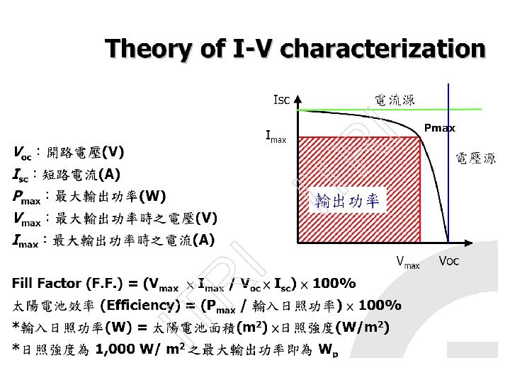
IV curve of a solar cell Voc (open circuit voltage) -when output current approaches zero, the voltage develops between two terminals ideally Voc~Eg at 0 K and inverse proportional to temperature Jsc (short-circuit current) -like the device connect the device with metal circuit, close to photogenerated current FF (fill factor): We want FF close to 1
Solar cell efficiency : an example J(m. A/cm 2) η and FF in this device ? 10 9 8 Jsc 7 (0. 55, 5. 9716) 6 5 η=PMP /Pin x 100%=FF*Voc. Jsc/ Pin x 100% (輸出電功率/入射光功率) P in =100 m. W/cm 2 PMP=VMP*JMP=0. 55*5. 9716=3. 28 m. W/cm 2 η =3. 28/100*100%=3. 28% JMP 4 3 2 1 0 0 0. 2 0. 4 VMP 0. 6 Voc 0. 8 1 Voc=0. 72 V Jsc=7. 1464 m. A/cm 2 FF=VMP*JMP/Voc*Jsc V(V) =3. 28/(0. 72*7. 14)=0. 63 Voc: 開路電壓 (open circuit voltage), 當輸出電流趨近於零,相 對太陽電池兩電極端點沒有連接所得到的電壓 Jsc: 短路電流(short circuit current) 如將照光的pn二極體兩端的金屬電極用金屬線連接, 造成短路, 此短路電流等於光電流
Theoretical efficiency limit
Various losses of solar energy of a Si solar cell during processing Silicon band gap is 1. 1 e. V, and the device loses all photon energy less than 1. 1 e. V Only 43. 6% remaining! - Excessive photon energy loss -Crystal surfaces and interfaces Contain a high concentration of Recombination centers Antireflection coating is not perfect Voc is inverse proportional to temperature, so not equals to Eg device fabrication resistance The highest efficient of a real photovoltaic device that uses a single crystal of Si Is about 24. 7% (澳洲新南威爾斯 大學)
Next step of crystalline Si solar cell
Various solar cells crystalline single crystalline polycrystalline silicon thin film amorphous solar cells compound organic single crystalline III-V(Ga. As) poly crystalline thin film CIGS dye sensitized polymer Cd. Te
Thin film solar cell: use Si as an example - required thickness of thin film solar cell is around 0. 5 μm, 1/500 of that of wafer based solar cell - material cost is very low
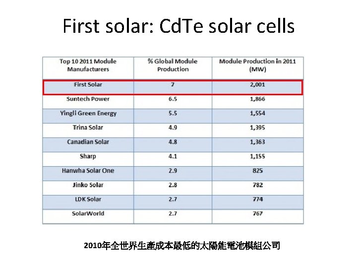
Photovoltaic materials and their cell ηcomparison High Cost Thin film solar cell Materials s-Si or poly a-Si Si Cd. Te CIGS manufacturin g process Crystal growth PECVD Sublimation Evaporation /selenizatio n Cell efficiency 21% 13% 16% 19. 9% Potential for production cost <$1. 00/Watt Doubtful Fair Good Very good Flexible modules No Yes No (rigid packing) Yes Stability Very good Intrinsic degradation Contact degradation No known degradation Remarks Shortage of raw Si wafer manufactruin g is xpensive -poor materials utilization Borderline efficienci after decades Need nonvaccum process for low lost production
Advantages of thin film solar cells 1. low raw materials are required for fabrication 2. light transmission is better 3. more competitive price (Cd. Te, US$1 per watt ; First Solar, stock price is US$180 ) 4. frameless design 5. Ideal for BIPV( building integrated photovoltaic)
(very short)
p-n junction and p-i-n junction
Amorphous Si solar cell : illustration 圖 6. 7 -a-Si’s absorption coefficient at visible light is one order of magnitude than c-Si , so only 10 -30 nm is needed to capture most photon in the visible region -thickness of p and n type around 10 -30 nm, thickness of i layer is less than 500 nm
CVD
II-VI compound solar cell: Cd. Te Abbreviated periodic table I II III B Al Cu Zn Ga Ag Cd In IV C Si Ge Sn V N P As Sb VI O S Se Te II-VI group as light harvesting materials band gap of Cd. Te : 1. 5 e. V
Device structure of Cd. Te solar cell P-type: Cd. Te n-type: Cd. S
I-III-VI 2 compound solar cells: Cu. In. Ga. Se(S) sphalerite structure I-III-VI group Abbreviated periodic table I II III B Al Cu Zn Ga Ag Cd In IV C Si Ge Sn V N P As Sb VI O S Se Te MI MII VI
Band gap and optical absorption of CIGS CISe 2: 1. 0 e. V CIGS: 1. 0 -1. 6 e. V CIS: 1. 3 -1. 5 e. V Muller, semiconductor for solar cells, 1993 Efficiency = FFVoc. Isc Pin -CIGS’s band gap is in the range of 1. 1 to 1. 5 ev
CIGS cell efficiency roadmap November, 2008 , Record Makes Thin-Film Solar Cell Competitive with Silicon Efficiency US National Renewable Energy Laboratory (NREL) CIGS solar cell reaches 20. 0% efficiency conversion
Cu(In, Ga)(S, Se)2 (CIGS) device structure Schematic picture Current collection grid HR-Zn. O/n+-Zn. O (0. 5µm) n-type. Cd. S (0. 05 µm) P-type Cu(In. Ga)Se 2 (2µm) Mo (0. 5 µm) Soda lime glass total device thickness less than 5 µm (Crystalline Si module~200 µm)
Vacuum-based techniques for CIGS film deposition Heater and substrate CIGS film deposition method: Multistage coevaporation process in a vacuum chamber Evaporation sources Drawbacks: -difficult to achieve controlled-stoichiometry over large device areas -manufacturing equipment is “very” expensive (> NT 0. 1 billion) -the deposition process is time-consuming -Highest efficiency (lab scale: 18~20%) -low materials utilization (30 -50%) -Usually UHV/MBE -low throughput -Cost prohibitive (but <cryst-Si)
Non-Vacuum Processing -Synthesize colloidal nanocrystals with controlled CIGS stoichiometry and deposit layer -Roll-to-roll manufractruing process 33
ISET’s non-vacuum process Substrate Efficiency Air Mass Soda lime Glass 13. 6% AM 1. 5 Molybdenum Foil 13. 0% AM 1. 5 Titanium foil 9. 5% AM 1. 5 Polyimide film 10. 4% AM 1. 5 Stainless Stell 9. 6% AM 1. 5 34 Kapur V. K. thin solid film, 2003
Nanosolar。破產, 2013年 7月
Process Silicon Vacuum. Wafer cells based thin film Si wafer High processing vacuum depositon Robust Fragile Process Yield Materials 30% Utilization Throughput 1 Roll-printed thin film Roll-to-roll printing Robust 30 -60% Over 97% 2 -5 10 -25
Comparison of three thin film solar cell Semiconductor Taiwan 2008
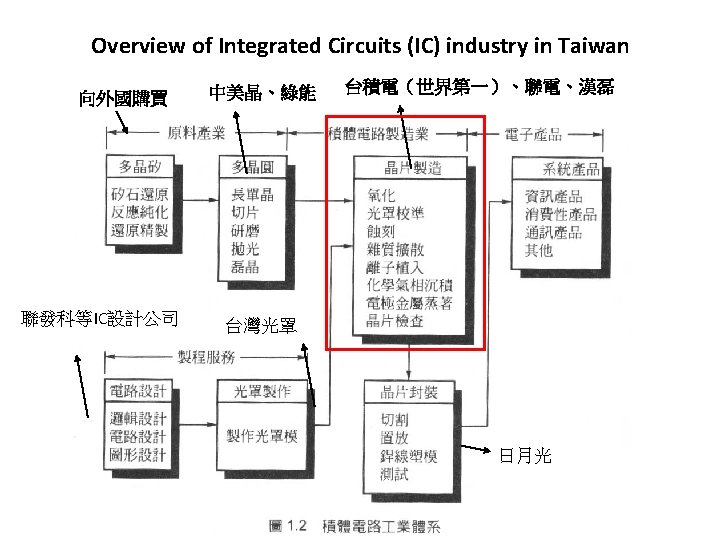
PV industry in Taiwan
PV industry in Taiwan
Market distribution in 2009
Today’s lecture references • Hitchman, M. L. and K. F. Jensen, “Chemical Vapor Deposition – principles and applications, ” ed. , Academic Press, San Diego, USA, 1993 • Zant, P. V. , “Microchip Fabrication, ” Mc. Graw. Hill, New York, 4 th ed. , 2000 • 林明獻, “矽晶圓半導體材料技術, ” 全華科技 圖書, 台北, 2007
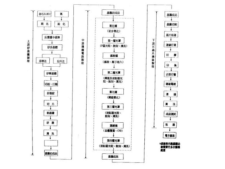
Si, Si, why Silicon? ? ? Silicon has smallest carrier mobility compared with Ge and Ga. As. Drawback of Ge -Ge’s device easily to leak at high temp. -Ge. O 2 is water soluble -melting point of Ge is only 937 C Drawback of Ga. As -hard to get high quality and large size wafer -need additional procedures to form dielectic materials Advantage of Si -Cheap raw materials, e. g. , rock, sand, second most abundant element on earth, appear as Si. O 2 - High melting point: 1415 C - stable silicon oxide (Si. O 2) as dielectric materials
Pizza vs microchip fabrication
RCA clean for silicon wafer surface Contamination includes organics, metals, and silicon oxide Organic clean: remove insoluble organic contaminants -solution: H 2 O 2: NH 4 OH with 5: 1: 1 Oxide Strip: remove thin silicon dioxide layer -solution: H 2 O: HF with 50: 1 Ionic Clean: remove ionic and heavy metal ionics contaminants -solution: H 2 O 2: HCl with 6: 1: 1 Like a baby
MOS transistor Passivation layer n metal layer P n Oxide layer -A MOS (Metal-oxide-semiconductor) transistor consists of different metal, oxide, and semiconductor layers. Intel's 65 nm n. MOS transistor
Four wafer-fabrication operations Grown Si. O 2 Layering -Add metal, insulator, semiconductor thin layers onto the wafer surface Patterning -form pattern by removing selected portions of added surface layers Doping -incorporate dopants into a wafer deposited layers hole island diffusion Ion implantation Heat treatment -remove contaminates, repair crystal structure of treated wafers annealing
Layering Grown Si. O 2 Passivation layer metal layer deposited layers n P n Various layering methods were developed to layer a thin film on a wafer Materials -Metal, oxide, and semiconductor Oxide layer
Layering materials and methods (CVD) (PVD) Methods include: thermal oxidation, chemical vapor deposition, evaporation, electroplating, and sputtering Ref. : Zant p 77
Thermal oxidation mechanism (layering) Si (solid) +O 2 (gas) Si. O 2 (solid) -Growth of Si. O 2 between 900 -1200 C -Control thickness of Si. O 2 layer depending on applications including surface passivation , doping barrier and device dielectric Silicon dioxide growth states initial linear parabolic -Si. O 2 growth stage *Linear growth oxygen atoms combine readily with the silicon atoms X=B/A*t *Parabolic growth oxygen needs to diffuse into the wafer react with Si (diffusion limited reaction X=(Bt)1/2 X=oxide thickness B=parabolic rate constant B/A=linear rate constant t = oxidation time Zant P 164
Patterning Passivation layer n metal layer P n Oxide layer hole island -Create the desired shapes in the exact dimensions required by the circuit design -Locate them in their proper location on the wafer surface and in relation to the other parts -the most critical step of the four basic operations, typically need 20 -40 individual patterning steps
Patterning = photolithography+etching Photo mask resist etching projection remove -Put a photoresist (here is negative resist) by spinning coating on the surface of oxide layer -Put a photomask on the top of wafer and expose the layer to the light -Negative resist undergoes polymerization when exposed to light -Development of unexposed photoresist -Etch exposed oxide layer -Remove the photoresist again development
photomask and photoresist Photoresist polarity Negative Clear field dark field Mask-reticle polarities Photoresist polarity -negative: polymerize when exposing to light -positive: not polymerize when exposing to light Positive hole island hole An example: Clear field result negative photoresist hole
Coating of photoresisit spread spin even faster Uniform thin film
Ten steps patterning process 1. Surface preparation – clean and dry wafer surface 2. Photoresist apply – spin coat a thin layer of photoresist on surface 3. Softbake - partial evaporation of photoresist solvents by heating 4. Alignment and exposure – Precise alignment of mask, exposure of photoresist 5. Development – Removal of unpolymerized resist 6. Hard bake – Additional evaporation of solvents 7. Develop inspect – inspect surface and check alignment and defects 8. Etch – Removal of top layer of wafer 9. Photoresist – remove photoresist layer from wafer 10. Final inspection – Surface inspection
Doping • Incorporate specific amounts of electrically active dopants (p-type or n-type) into the wafer surface • Formation of P-N junction • Doping techniques - thermal diffusion - ion implantation
Formation of P-N junction by doping P-type wafer made before -Junction- the location where the number of N-type and P-type dopants are equal -PN junction is very important for making field effect transistor (FET), Light emitting diode (LED), solar cell etc….
Doping by thermal diffusion Diffusion : -the movement of one material through another due to concentration gradient -continue until the concentration is under equilibrium Thermal diffusion : -deposition and drive-in oxidation
Thermal diffusion with Deposition vancancy movement Diffusion rate is controlled by 1. diffusivity of particular dopant 2. maximum solid solubility Interstitial movement Deposition steps 1. Preclean and etch – etched in HF to remove oxide formed on the surface 2. Deposition – loading cycle, actual doping cycle, exit cycle, all under nitrogen 3. Deglaze – diluted HF to remove thin oxide layer formed in 2 4. Evaluation – test the electrical properties
Thermal diffusion – Drive-in Oxidation Redistribution of the dopant in the wafer -heat to drive the dopant atoms deeper and wider into the wafer Growth of a new oxide on the exposed silicon surface -perform the oxidation on the surface -operate as the oxidation process
Challenge of doping via thermal diffusion Challenge -lateral diffusion -ultra thin junction -poor doping control -surface contamination interference -dislocation generation, due to high temperature operation Future MOS transistor needs two requirements -Low dopant concentration control -Ultra thin junction
Ion implantation A physical process Like a cannon shoot a ball to penetrate the wall and go the inside of the wall Advantages -No side diffusion, operate at room temperature -good control of the dopants location -majority of doping steps for advanced circuits
Ion implantation system E- BF 3 B+ BF 2+. . etc -Ionization chamber : a electron created from a filament collide with the dopant source mass analyzing/ion selection by magnetic field -acceleration tube : accelerate the ion to a high velocity -neutral beam trap : collect netralized ions Challenge: lattice damage, damage cluster, and vacancy-interstitial
Heat treatment Goals: • to heal the wafer damage due to ion implantation: anneal the wafer at 1000 C to recover the crystal structure • To alloy metal with Si to metalsilide as electrical contact at about 450 C • To soft bake or hard bake the wafers with photoresisit layers • Deposition
Silicon gate MOS transistor process steps: combination of four basic operations layering Pattering, layering, , heat treatment , doping patterning, layering passivation layer n P metal layer n Oxide layer
Packaging http: //www. siliconimaging. com Procedures -Die separation -lead bonding -chip/package connection -enclosure -Glod wire bonding
Integrated circuits (ICs) - Combination of transistors, diodes, capacitors in a chip - Ultra large scale integration (ULSI) >1, 000 components per chips - Morre’s law: the number of transistors on a chip were doubling every 18 months - Intel four core Itanium CPU- Tukwila has over 2 billion transistors on a chip Courtesy of wiki
Cleanroom Class maximum particles/ft³(0. 027 m 3) ISO ≥ 0. 1 µm ≥ 0. 2 µm ≥ 0. 3 µm ≥ 0. 5 µm ≥ 5 µm equivalent 1 35 7 3 1 ISO 3 10 350 75 30 10 ISO 4 750 300 100 ISO 5 100 1, 000 7 ISO 6 10, 000 70 ISO 7 100, 000 700 ISO 8 How clean? Ex: The land area of Taiwan: 35960 km 2 190 km so there is only one particle larger than 0. 3 m -Most of IC devices are made in class 1 clean room Courtesy of wiki
Clean cloth
Work environment