Fundamentals of Optoelectronic Materials and Devices HsingYu Tuan
 Department of Chemical Engineering,")


 -We build a optical cavity to trap the wavelength")


")


 Theoretical maximum efficiency of a semiconductor S(λ) =# of")
 vs Eg (e. V) under AM 1. 5 real ηmax is only around")


 Bus electrode (2) for current collection")
 develops between the terminals")
 -when output current approaches")
 η and FF in this")


")


 sphalerite structure I-III-VI group Abbreviated")


(S, Se)2 (CIGS) device structure Schematic picture Current collection grid HR-Zn. O/n+-Zn. O")


- Slides: 70
Fundamentals of Optoelectronic Materials and Devices 光電材料與元件基礎 Hsing-Yu Tuan (段興宇) Department of Chemical Engineering, National Tsing. Hua University
Fabrication of laser diode using pn junction structures Laser: Light Amplification by Stimulated Emission of Radiation
Two keys for making a laser population inversion Optical cavity
Absorption, spontaneous, and stimulated emission Emission: an electron at a higher energy level transits down to an unoccupied energy level and it emits a photon Spontaneous emission: emitted photon from E 2 to E 1 in a random direction, which provided by the E 1 not already occupied by another electron Stimulated emission: 1. Emitted photon is in phase with incoming photon (the same direction, the same energy, the same polarization) 2. Incoming photons was magnified there are more atoms at E 2 than at E 1 (population inversion), so incoming photons were not absorbed by another atom at E 1 The key 1 of laser: population inversion
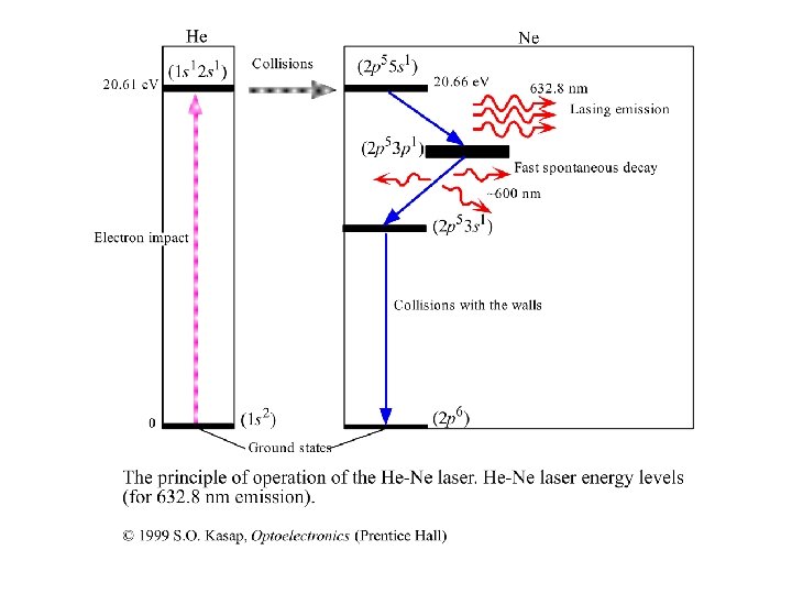
The way to achieve population inversion Note: -in normal case, only two energy levels can not achieve population inversion -external excitation first excite electron from E 1 to E 3 -the emission from E 2 to E 1 is called lasing emission -LASER: Light Amplification by Stimulated Emission of Radiation - an example: Cr+3 ion in a crystal of alumina Al 2 O 3 (saphire)
Er+3 doped glas fiber : an example
Make Stimulated emission rate larger Spontaneous emission Stimulated emission R 21 - downward transition rate from E 2 to E 1 R 21 = A 21 N 2+B 21 N 2 (hv) Spontaneous emission Stimulated emission which requires Photons to drive it stimulated spontaneous We need a large photon concentration with the wavelength we want! - Need an optical cavity -photon energy density per unit frequency -the number of photons per unit volume with an energy hv=(E 2 -E 1)
A optical cavity (optical resonator) -We build a optical cavity to trap the wavelength we want -only standing waves with certain wavelength can be maintained within the optical cavity m: mode number (an interger) Wavelength satisfy the left equation is called A cavity mode
Laser diodes: utilization of PN junction • Compared to other lasers (sapphire, CO 2, He. Ne, dye), semiconductor laser diodes are compact in size, electricity effective, efficient, long life, cheap, and versatile in color from UV to IR. • Applications – CD, VCD, DVD players, CDROM, laser printer, laser pointer, bar code scanner, etc.
Degenerated semiconductor -the semiconductor that was excessively doped with donors or acceptors (10 19 -1020 cm-3) called degenerate semiconductor -such a semiconductor exhibits properties that are more metal-like -degenerate doping: the Fermi level EFP in the p-side is in the valence band(VB) and the EFn in the n-side is in the conduction band (CB) -a laser diode consists of “degenerately” doped p+ side with “degenerated” doped n+ side (p+n+ junction)
Structure: degenerately doped direct bandgap semiconductor pn junction After applying large forward bias V LED -laser diode structure: degenerately doped direct bandgap semiconductor pn junction -depletion region (active region) is very narrow -population inversion occurs when applying a voltage larger e. V > Eg: the applied V diminishes the built-in potential to zero and electrons flow into the SCL -an incoming photon with energy Ec-Ev doesn’t excite an electron but stimulated by falling electrons
Density of States and optical Gain in the active layer -the active region has an optical gain since an incoming photon is more likely to cause stimulated emission than being absorbed -the pumping mechanism caused by forward diode current is called injection pumping -the pumping energy is supplied by the external battery
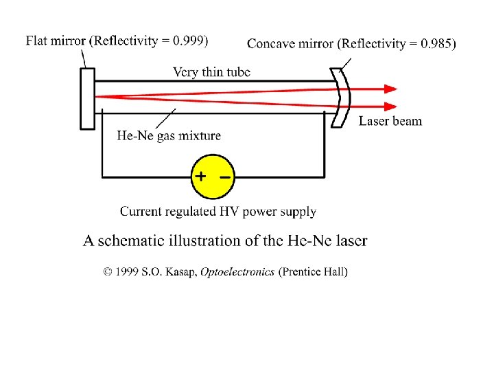
Build an optical resonator in a laser diode an optical resonator n: refractive index -an optical cavity (resonator)) is required to implement a laser oscillator to build up the intensity of stimulated emissions. -the ends of the crystal are cleaved to be flat and optically polished to provide reflection and form an optical resonator -this process can build up the intensity of the radiation in the cavity
Output power vs. diode current of a laser diode Threshold current -lasing radiation is only obtained when the optical gain in the medium can overcome the photon losses from the cavity, which requires the diode current I to exceed a threshold value Ith -below Ith: spontaneous emission; above Ith: stimulated emission
Comparison of laser’s and LED’s light power versus current
Heterostructure laser diode + + + -a heterostructured laser diode can significantly reduce threshold current (Ith) -we confine the injected electrons and holes to a narrow region, so that less current is needed to make population inversion -carriers are confined in the p-Ga. As (active area) when the voltage is applied -ga. As layer is very thin, so the concentration of injected electrons can be increased quickly with moderate increases in forward current.
Schematic illustration of a double heterojunction laser diode
photovoltaic device (solar cell)
Solar cells Solar light in Electricity out
Generate electrons from materials by photons • Semiconductor, polymer or dyes excited state Conduction band or HOMO Valence band or LUMO Separation of the electron-hole pair electron Conduction band or HOMO pair Valence band or LUMO So, materials used for solar cell application need to have discrete energy gap for photogeneration of electron-hole pair
Elemental and Compound Semiconductors I II 29 Cu 47 Ag 30 Zn 48 Cd III 5 B 13 Al 31 Ga 49 In IV 6 C 14 Si 32 Ge 50 Sn V 7 N 15 P 33 As 51 Sb VI 8 O 16 S 34 Se 52 Te 24
Pick right materials - Good absorption coefficient to harvest light - Suitable band gap
Absorption of semiconductors Phonon emission o r absorption -We prefer direct semiconduct materials since they can absorb light more efficiently -Si and Ge’s absorption coefficient increase slowly with increased energy
Pick suitable Eg (e. V) Theoretical maximum efficiency of a semiconductor S(λ) =# of photons/area*time -bandgap of semiconductor should not be wide get higher S(λ) -Electrons in the valence band can absorb energy of Eg, 2 Eg, 3 Eg, but the excess energy can not be transformed to electric energy but transform to heat need higher Eg -very narrow band gap material can absorb most wavelength from sun, but transformed energy is small.
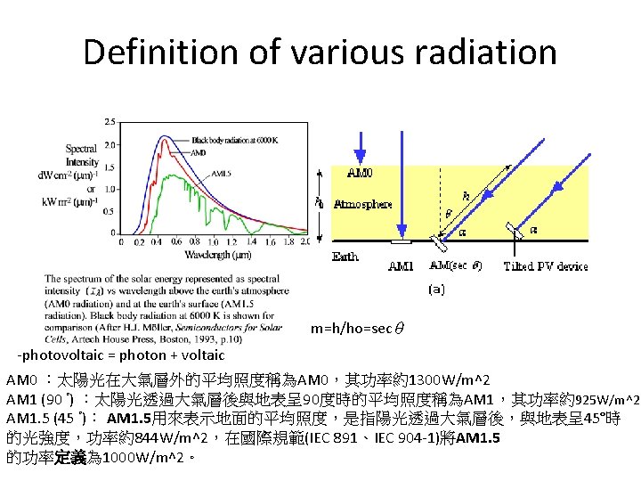
ηmax(%) vs Eg (e. V) under AM 1. 5 real ηmax is only around 30% due to loss of other facters Eg: 1. 0 – 1. 5 e. V is the best range
Absorption of semiconductor Phonon emission o r absorption -We prefer direct semiconduct materials since they can absorb light more efficiently -Si and Ge’s absorption coefficient increase slowly with increased energy
A PN junction photovoltaic device -incoming photon generate EHPs and separated by the build-in field Eo, drifts them apart -generated electrons and hole can diffuse and drift in neural region and SCL, respectively -
A PN junction photovoltaic device -The movement of minority carriers is critical for the amount of generated current -Without Eo it is not possible to drift apart the photogenerated EHPs accumulate excess electrons on the n-side and excess holes on the p-side
A PN junction photovoltaic device 0. 2 μm 200 -500 μm : life time Electron diffusion length -Silicon’s electron diffusion length is longer than the hole diffusion length -we make a device with very narrow n region and longer p region -n side: 0. 2 μm or less ; p-side: 200 -500 μm Reason: (1) the electron diffusion length in Si Is longer than the dole diffusion length Only electrons within the Le to the depletion (2) At long wavelengths, around 1 -1. 2 μm, the Layer can contribute to the photovoltaic effect absorption coefficient α of Si is small and the absorption depth (1/ α) is typically greater than 100 μm.
Photogenerated carriers within the solar cell At Photocurrent Iph = e. Go. A(ln + W+Le) Go = photogeneration rate
Device structure of a Si solar cell (1) Bus electrode (2) for current collection Finger electrodes 0. 2 μm n 200 μm p (3) surface texturization Incident light In order to capture more light and to allow more photons into the device - finger electrodes were made to allow light pass through the device - a thin antireflection coating on the surface reduces light reflection and allow more lighte to enter the device -surface texturization to for multiple light reflection and increase light path
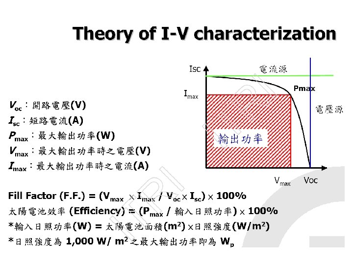
Voc and Jsc metal conductor Short circuit Open-circuit voltage (Voc) develops between the terminals of the device because the electron reaches the neutral n and p, respectively. -An external load (metal) is connected To the cell, and is a short circuit called short circuit current – the maximum photocurrent
IV curve of a solar cell Voc (open circuit voltage) -when output current approaches zero, the voltage develops between two terminals ideally Voc~Eg at 0 K and inverse proportional to temperature Jsc (short-circuit current) -like the device connect the device with metal circuit, close to photogenerated current FF (fill factor): We want FF close to 1
Solar cell efficiency : an example J(m. A/cm 2) η and FF in this device ? 10 9 8 Jsc 7 (0. 55, 5. 9716) 6 5 JMP 4 3 2 1 0 0 0. 2 0. 4 VMP 0. 6 Voc 0. 8 1 η=PMP /Pin x 100%=FF*Voc. Jsc/ Pin x 100% (輸出電功率/入射光功率) P in =100 m. W/cm 2 PMP=VMP*JMP=0. 55*5. 9716=3. 28 m. W/cm 2 η =3. 28/100*100%=3. 28% Voc=0. 72 V Jsc=7. 1464 m. A/cm 2 FF=VMP*JMP/Voc*Jsc V(V) =3. 28/(0. 72*7. 14)=0. 63 Voc: 開路電壓 (open circuit voltage), 當輸出電流趨近於零,相 對太陽電池兩電極端點沒有連接所得到的電壓 Jsc: 短路電流(short circuit current) 如將照光的pn二極體兩端的金屬電極用金屬線連接, 造成短路, 此短路電流等於光電流
Theoretical efficiency limit
Various losses of solar energy of a Si solar cell during processing Silicon band gap is 1. 1 e. V, and the device loses all photon energy less than 1. 1 e. V Only 43. 6% remaining! - Excessive photon energy loss -Crystal surfaces and interfaces Contain a high concentration of Recombination centers Antireflection coating is not perfect Voc is inverse proportional to temperature, so not equals to Eg device fabrication resistance The highest efficient of a real photovoltaic device that uses a single crystal of Si Is about 24. 7% (澳洲新南威爾斯 大學)
Next step of crystalline Si solar cell
Various solar cells crystalline single crystalline polycrystalline silicon thin film amorphous solar cells compound organic single crystalline III-V(Ga. As) poly crystalline thin film CIGS dye sensitized polymer Cd. Te
Thin film solar cell: use Si as an example - required thickness of thin film solar cell is around 0. 5 μm, 1/500 of that of wafer based solar cell - material cost is very low
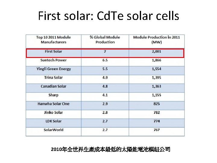
Photovoltaic materials and their cell ηcomparison High Cost Thin film solar cell Materials s-Si or poly a-Si Si Cd. Te CIGS manufacturin g process Crystal growth PECVD Sublimation Evaporation /selenizatio n Cell efficiency 21% 13% 16% 19. 9% Potential for production cost <$1. 00/Watt Doubtful Fair Good Very good Flexible modules No Yes No (rigid packing) Yes Stability Very good Intrinsic degradation Contact degradation No known degradation Remarks Shortage of raw Si wafer manufactruin g is xpensive -poor materials utilization Borderline efficienci after decades Need nonvaccum process for low lost production
Advantages of thin film solar cells 1. low raw materials are required for fabrication 2. light transmission is better 3. more competitive price (Cd. Te, US$1 per watt ; First Solar, stock price is US$180 ) 4. frameless design 5. Ideal for BIPV( building integrated photovoltaic)
(very short)
p-n junction and p-i-n junction
Amorphous Si solar cell : illustration 圖 6. 7 -a-Si’s absorption coefficient at visible light is one order of magnitude than c-Si , so only 10 -30 nm is needed to capture most photon in the visible region -thickness of p and n type around 10 -30 nm, thickness of i layer is less than 500 nm
CVD
II-VI compound solar cell: Cd. Te Abbreviated periodic table I II IV V VI B C N O Al Si P S Cu Zn Ga Ge As Se Ag Cd In Sn Sb Te II-VI group as light harvesting materials band gap of Cd. Te : 1. 5 e. V
Device structure of Cd. Te solar cell P-type: Cd. Te n-type: Cd. S
I-III-VI 2 compound solar cells: Cu. In. Ga. Se(S) sphalerite structure I-III-VI group Abbreviated periodic table I II IV V VI B C N O Al Si P S Cu Zn Ga Ge As Se Ag Cd In Sn Sb Te MI MII VI
Band gap and optical absorption of CIGS CISe 2: 1. 0 e. V CIGS: 1. 0 -1. 6 e. V CIS: 1. 3 -1. 5 e. V Muller, semiconductor for solar cells, 1993 Efficiency = FFVoc. Isc Pin -CIGS’s band gap is in the range of 1. 1 to 1. 5 ev
CIGS cell efficiency roadmap November, 2008 , Record Makes Thin-Film Solar Cell Competitive with Silicon Efficiency US National Renewable Energy Laboratory (NREL) CIGS solar cell reaches 20. 0% efficiency conversion
Cu(In, Ga)(S, Se)2 (CIGS) device structure Schematic picture Current collection grid HR-Zn. O/n+-Zn. O (0. 5µm) n-type. Cd. S (0. 05 µm) P-type Cu(In. Ga)Se 2 (2µm) Mo (0. 5 µm) Soda lime glass total device thickness less than 5 µm (Crystalline Si module~200 µm)
Vacuum-based techniques for CIGS film deposition Heater and substrate CIGS film deposition method: Multistage coevaporation process in a vacuum chamber Evaporation sources Drawbacks: -difficult to achieve controlled-stoichiometry over large device areas -manufacturing equipment is “very” expensive (> NT 0. 1 billion) -the deposition process is time-consuming -Highest efficiency (lab scale: 18~20%) -low materials utilization (30 -50%) -Usually UHV/MBE -low throughput -Cost prohibitive (but <cryst-Si)
Non-Vacuum Processing -Synthesize colloidal nanocrystals with controlled CIGS stoichiometry and deposit layer -Roll-to-roll manufractruing process 60
ISET’s non-vacuum process Substrate Efficiency Air Mass Soda lime Glass 13. 6% AM 1. 5 Molybdenum Foil 13. 0% AM 1. 5 Titanium foil 9. 5% AM 1. 5 Polyimide film 10. 4% AM 1. 5 Stainless Stell 9. 6% AM 1. 5 61 Kapur V. K. thin solid film, 2003
Nanosolar。破產, 2013年 7月
Process Silicon Vacuum. Wafer cells based thin film Si wafer High processing vacuum depositon Robust Fragile Process Yield Materials 30% Utilization Throughput 1 Roll-printed thin film Roll-to-roll printing Robust 30 -60% Over 97% 2 -5 10 -25
Comparison of three thin film solar cell Semiconductor Taiwan 2008
PV industry in Taiwan
PV industry in Taiwan
Market distribution in 2009