Fundamentals of Optoelectronic Materials and Devices HsingYu Tuan



- Slides: 62
Fundamentals of Optoelectronic Materials and Devices 光電材料與元件基礎 Hsing-Yu Tuan (段興宇) Department of Chemical Engineering, National Tsing. Hua University
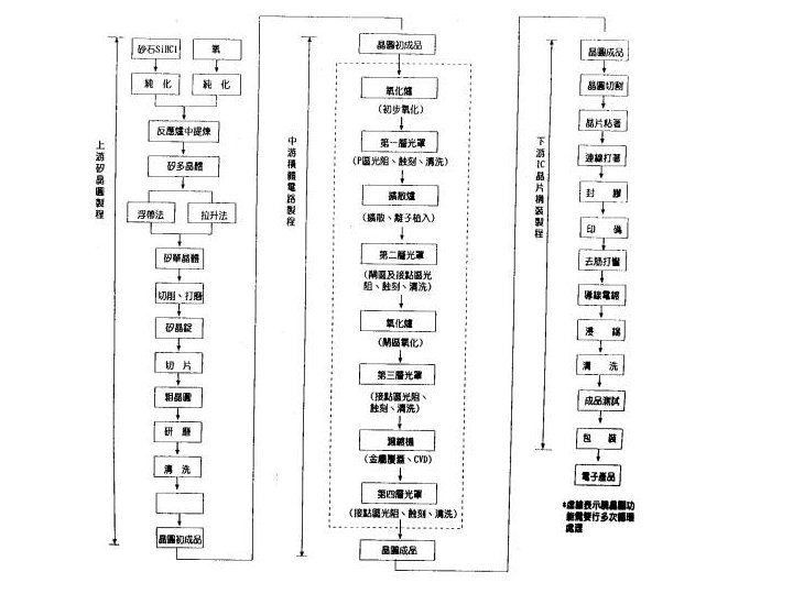
Today’s lecture references • Hitchman, M. L. and K. F. Jensen, “Chemical Vapor Deposition – principles and applications, ” ed. , Academic Press, San Diego, USA, 1993 • Zant, P. V. , “Microchip Fabrication, ” Mc. Graw. Hill, New York, 4 th ed. , 2000 • 林明獻, “矽晶圓半導體材料技術, ” 全華科技 圖書, 台北, 2007
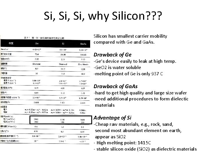
Si, Si, why Silicon? ? ? Silicon has smallest carrier mobility compared with Ge and Ga. As. Drawback of Ge -Ge’s device easily to leak at high temp. -Ge. O 2 is water soluble -melting point of Ge is only 937 C Drawback of Ga. As -hard to get high quality and large size wafer -need additional procedures to form dielectic materials Advantage of Si -Cheap raw materials, e. g. , rock, sand, second most abundant element on earth, appear as Si. O 2 - High melting point: 1415 C - stable silicon oxide (Si. O 2) as dielectric materials
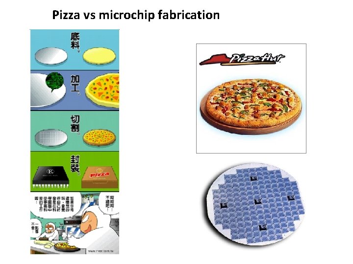
Pizza vs microchip fabrication
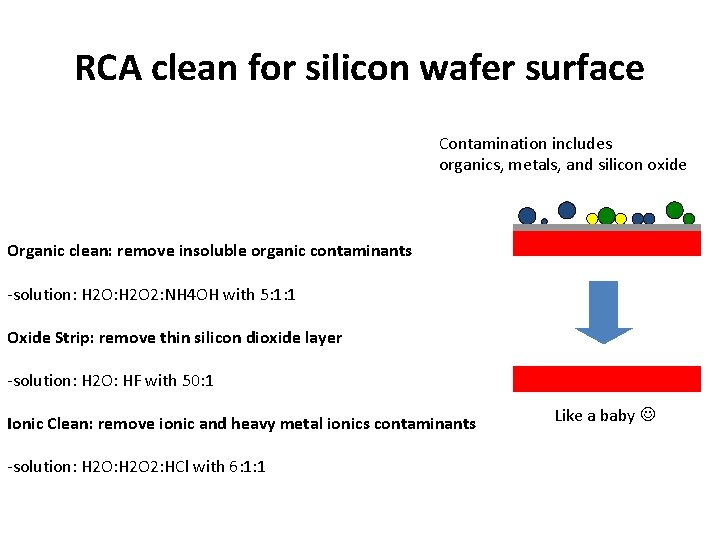
RCA clean for silicon wafer surface Contamination includes organics, metals, and silicon oxide Organic clean: remove insoluble organic contaminants -solution: H 2 O 2: NH 4 OH with 5: 1: 1 Oxide Strip: remove thin silicon dioxide layer -solution: H 2 O: HF with 50: 1 Ionic Clean: remove ionic and heavy metal ionics contaminants -solution: H 2 O 2: HCl with 6: 1: 1 Like a baby
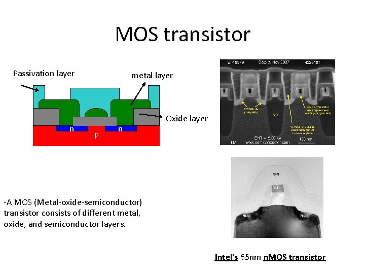
MOS transistor Passivation layer n metal layer P n Oxide layer -A MOS (Metal-oxide-semiconductor) transistor consists of different metal, oxide, and semiconductor layers. Intel's 65 nm n. MOS transistor
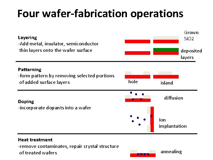
Four wafer-fabrication operations Grown Si. O 2 Layering -Add metal, insulator, semiconductor thin layers onto the wafer surface Patterning -form pattern by removing selected portions of added surface layers Doping -incorporate dopants into a wafer deposited layers hole island diffusion Ion implantation Heat treatment -remove contaminates, repair crystal structure of treated wafers annealing
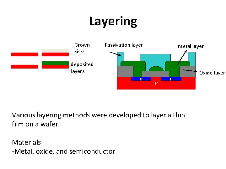
Layering Grown Si. O 2 Passivation layer metal layer deposited layers n P n Various layering methods were developed to layer a thin film on a wafer Materials -Metal, oxide, and semiconductor Oxide layer
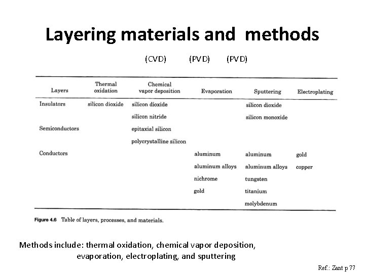
Layering materials and methods (CVD) (PVD) Methods include: thermal oxidation, chemical vapor deposition, evaporation, electroplating, and sputtering Ref. : Zant p 77
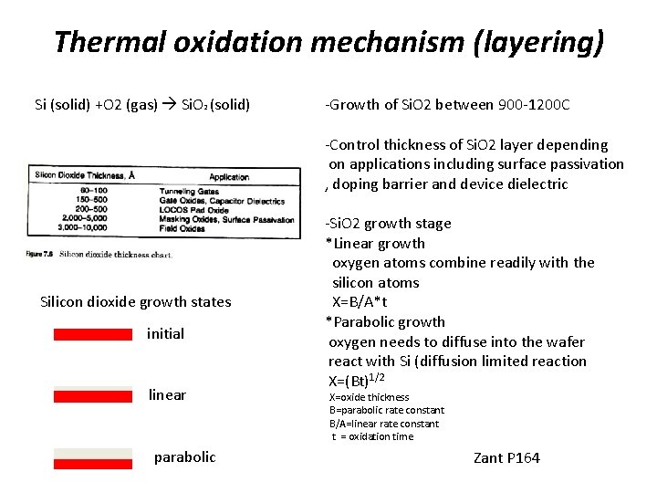
Thermal oxidation mechanism (layering) Si (solid) +O 2 (gas) Si. O 2 (solid) -Growth of Si. O 2 between 900 -1200 C -Control thickness of Si. O 2 layer depending on applications including surface passivation , doping barrier and device dielectric Silicon dioxide growth states initial linear parabolic -Si. O 2 growth stage *Linear growth oxygen atoms combine readily with the silicon atoms X=B/A*t *Parabolic growth oxygen needs to diffuse into the wafer react with Si (diffusion limited reaction X=(Bt)1/2 X=oxide thickness B=parabolic rate constant B/A=linear rate constant t = oxidation time Zant P 164
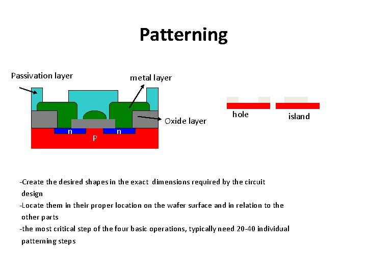
Patterning Passivation layer n metal layer P n Oxide layer hole island -Create the desired shapes in the exact dimensions required by the circuit design -Locate them in their proper location on the wafer surface and in relation to the other parts -the most critical step of the four basic operations, typically need 20 -40 individual patterning steps
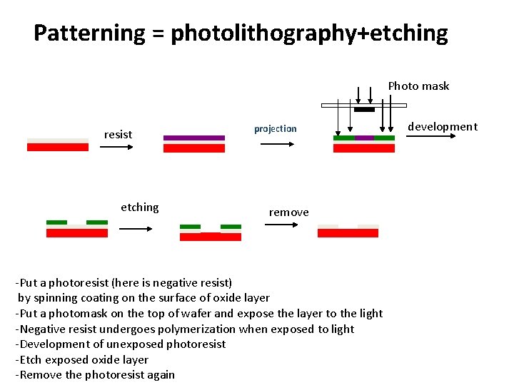
Patterning = photolithography+etching Photo mask resist etching projection remove -Put a photoresist (here is negative resist) by spinning coating on the surface of oxide layer -Put a photomask on the top of wafer and expose the layer to the light -Negative resist undergoes polymerization when exposed to light -Development of unexposed photoresist -Etch exposed oxide layer -Remove the photoresist again development
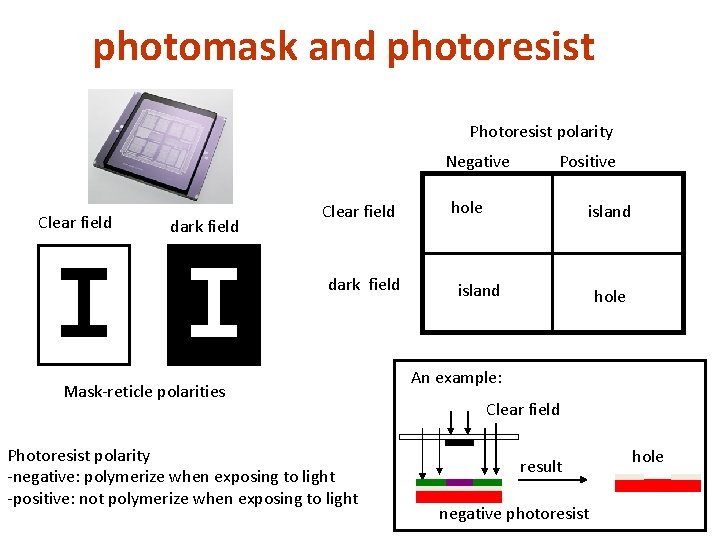
photomask and photoresist Photoresist polarity Negative Clear field dark field Mask-reticle polarities Photoresist polarity -negative: polymerize when exposing to light -positive: not polymerize when exposing to light Positive hole island hole An example: Clear field result negative photoresist hole
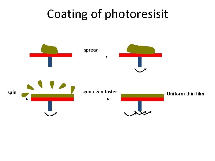
Coating of photoresisit spread spin even faster Uniform thin film
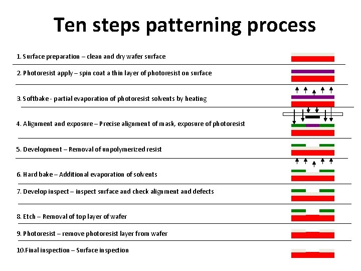
Ten steps patterning process 1. Surface preparation – clean and dry wafer surface 2. Photoresist apply – spin coat a thin layer of photoresist on surface 3. Softbake - partial evaporation of photoresist solvents by heating 4. Alignment and exposure – Precise alignment of mask, exposure of photoresist 5. Development – Removal of unpolymerized resist 6. Hard bake – Additional evaporation of solvents 7. Develop inspect – inspect surface and check alignment and defects 8. Etch – Removal of top layer of wafer 9. Photoresist – remove photoresist layer from wafer 10. Final inspection – Surface inspection
Doping • Incorporate specific amounts of electrically active dopants (p-type or n-type) into the wafer surface • Formation of P-N junction • Doping techniques - thermal diffusion - ion implantation
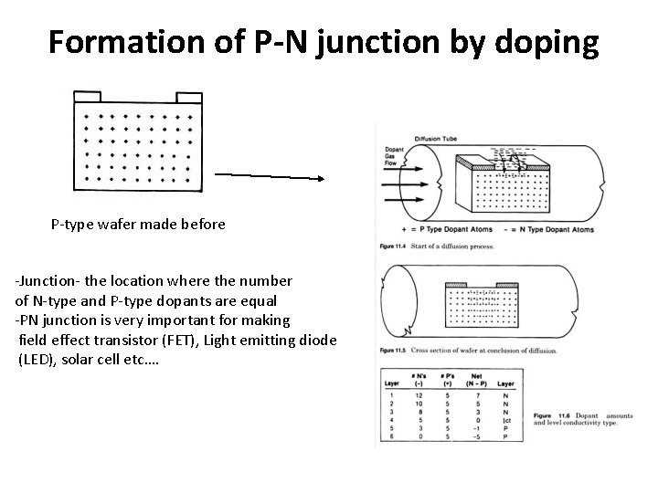
Formation of P-N junction by doping P-type wafer made before -Junction- the location where the number of N-type and P-type dopants are equal -PN junction is very important for making field effect transistor (FET), Light emitting diode (LED), solar cell etc….
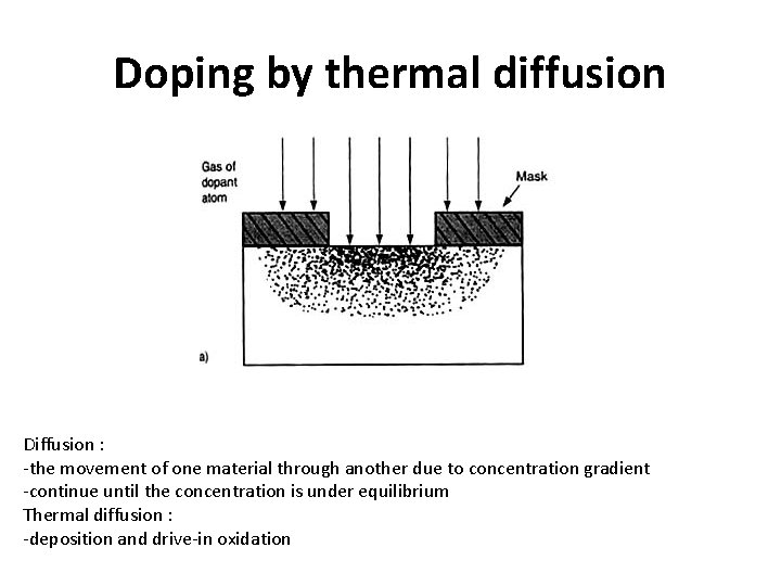
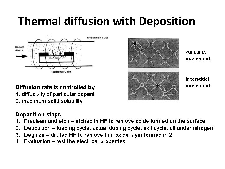
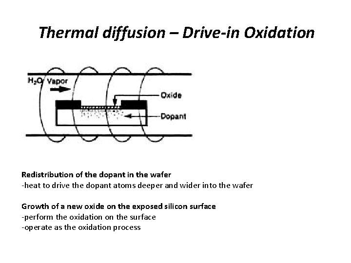
Doping by thermal diffusion Diffusion : -the movement of one material through another due to concentration gradient -continue until the concentration is under equilibrium Thermal diffusion : -deposition and drive-in oxidation
Thermal diffusion with Deposition vancancy movement Diffusion rate is controlled by 1. diffusivity of particular dopant 2. maximum solid solubility Interstitial movement Deposition steps 1. Preclean and etch – etched in HF to remove oxide formed on the surface 2. Deposition – loading cycle, actual doping cycle, exit cycle, all under nitrogen 3. Deglaze – diluted HF to remove thin oxide layer formed in 2 4. Evaluation – test the electrical properties
Thermal diffusion – Drive-in Oxidation Redistribution of the dopant in the wafer -heat to drive the dopant atoms deeper and wider into the wafer Growth of a new oxide on the exposed silicon surface -perform the oxidation on the surface -operate as the oxidation process
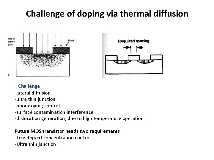
Challenge of doping via thermal diffusion Challenge -lateral diffusion -ultra thin junction -poor doping control -surface contamination interference -dislocation generation, due to high temperature operation Future MOS transistor needs two requirements -Low dopant concentration control -Ultra thin junction
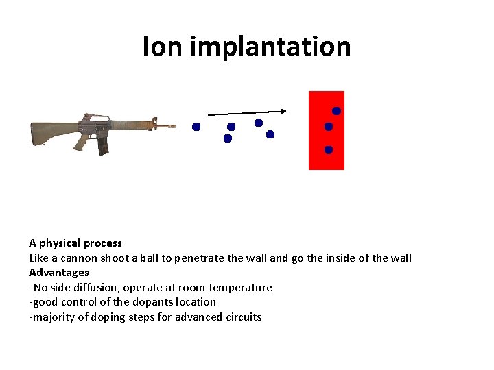
Ion implantation A physical process Like a cannon shoot a ball to penetrate the wall and go the inside of the wall Advantages -No side diffusion, operate at room temperature -good control of the dopants location -majority of doping steps for advanced circuits
Ion implantation system E- BF 3 B+ BF 2+. . etc -Ionization chamber : a electron created from a filament collide with the dopant source mass analyzing/ion selection by magnetic field -acceleration tube : accelerate the ion to a high velocity -neutral beam trap : collect netralized ions Challenge: lattice damage, damage cluster, and vacancy-interstitial
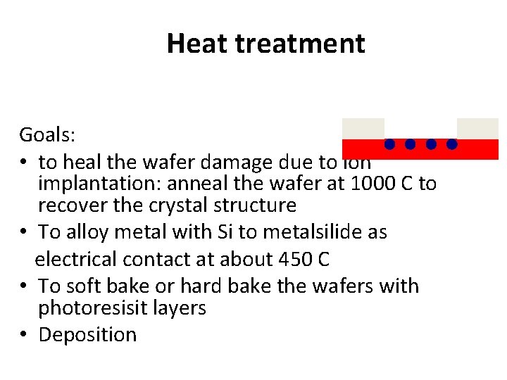
Heat treatment Goals: • to heal the wafer damage due to ion implantation: anneal the wafer at 1000 C to recover the crystal structure • To alloy metal with Si to metalsilide as electrical contact at about 450 C • To soft bake or hard bake the wafers with photoresisit layers • Deposition
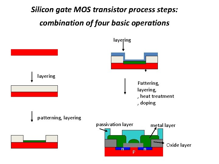
Silicon gate MOS transistor process steps: combination of four basic operations layering Pattering, layering, , heat treatment , doping patterning, layering passivation layer n P metal layer n Oxide layer
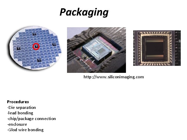
Packaging http: //www. siliconimaging. com Procedures -Die separation -lead bonding -chip/package connection -enclosure -Glod wire bonding
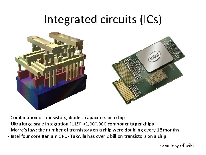
Integrated circuits (ICs) - Combination of transistors, diodes, capacitors in a chip - Ultra large scale integration (ULSI) >1, 000 components per chips - Morre’s law: the number of transistors on a chip were doubling every 18 months - Intel four core Itanium CPU- Tukwila has over 2 billion transistors on a chip Courtesy of wiki
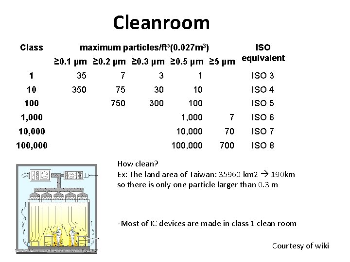
Cleanroom Class maximum particles/ft³(0. 027 m 3) ISO ≥ 0. 1 µm ≥ 0. 2 µm ≥ 0. 3 µm ≥ 0. 5 µm ≥ 5 µm equivalent 1 35 7 3 1 ISO 3 10 350 75 30 10 ISO 4 100 750 300 100 ISO 5 1, 000 7 ISO 6 10, 000 70 ISO 7 100, 000 700 ISO 8 How clean? Ex: The land area of Taiwan: 35960 km 2 190 km so there is only one particle larger than 0. 3 m -Most of IC devices are made in class 1 clean room Courtesy of wiki
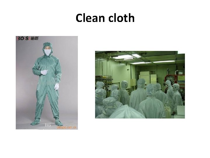
Clean cloth
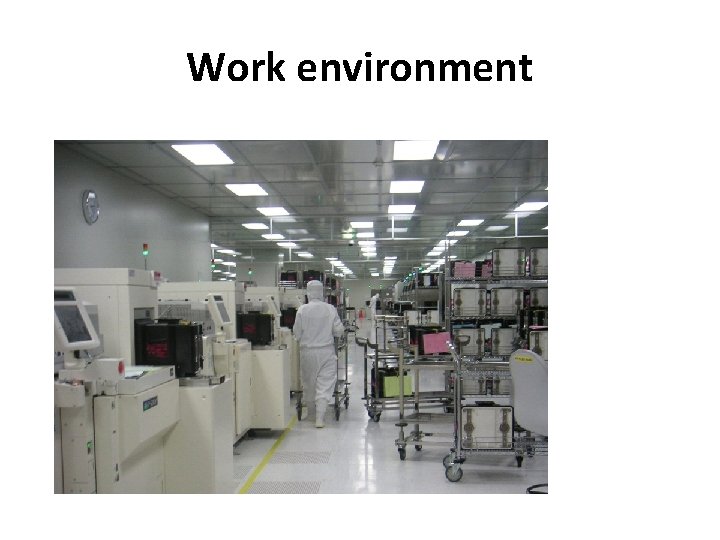
Work environment
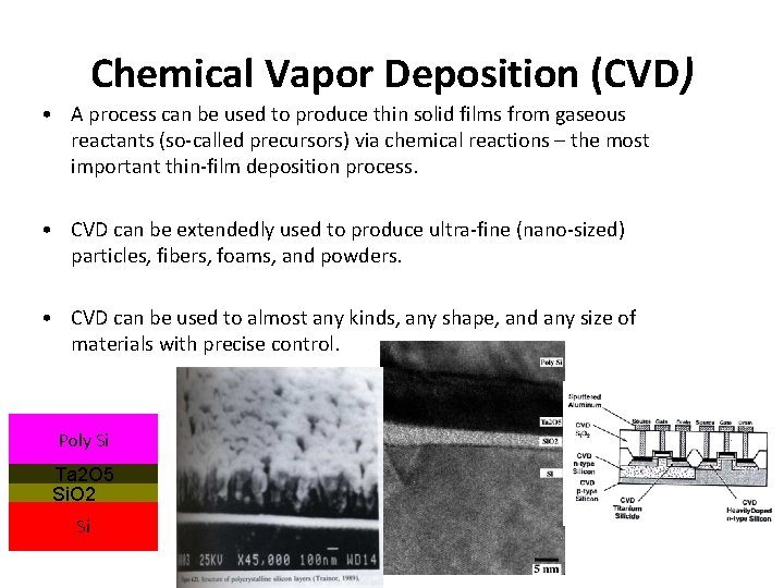
Chemical Vapor Deposition (CVD) • A process can be used to produce thin solid films from gaseous reactants (so-called precursors) via chemical reactions – the most important thin-film deposition process. • CVD can be extendedly used to produce ultra-fine (nano-sized) particles, fibers, foams, and powders. • CVD can be used to almost any kinds, any shape, and any size of materials with precise control. Poly Si Ta 2 O 5 Si. O 2 Si
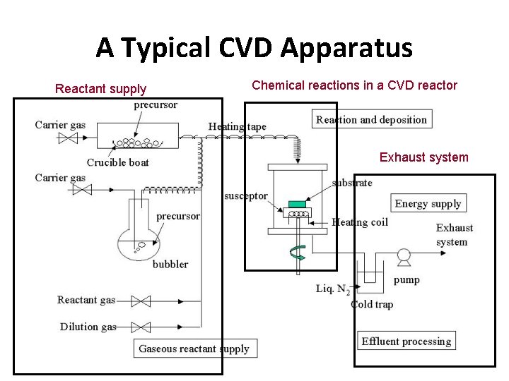
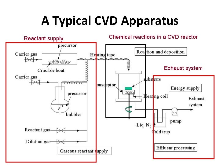
A Typical CVD Apparatus Reactant supply Chemical reactions in a CVD reactor Exhaust system
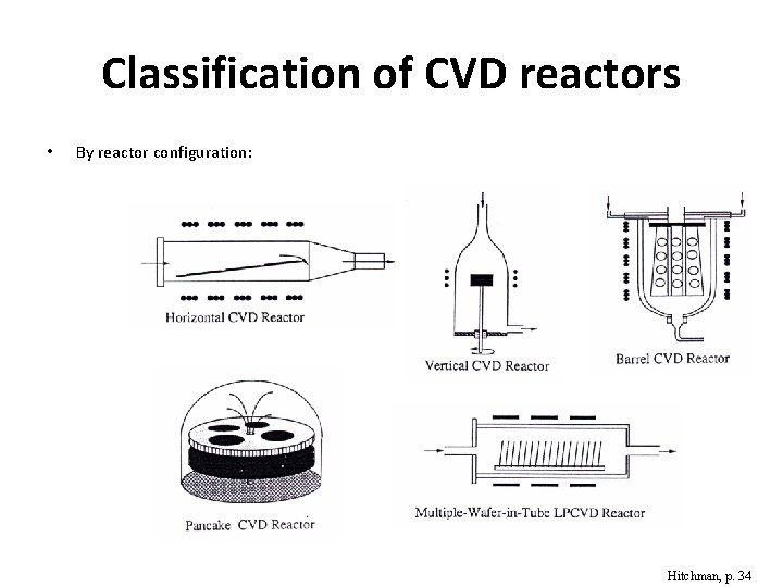
Classification of CVD reactors • By reactor configuration: Hitchman, p. 34
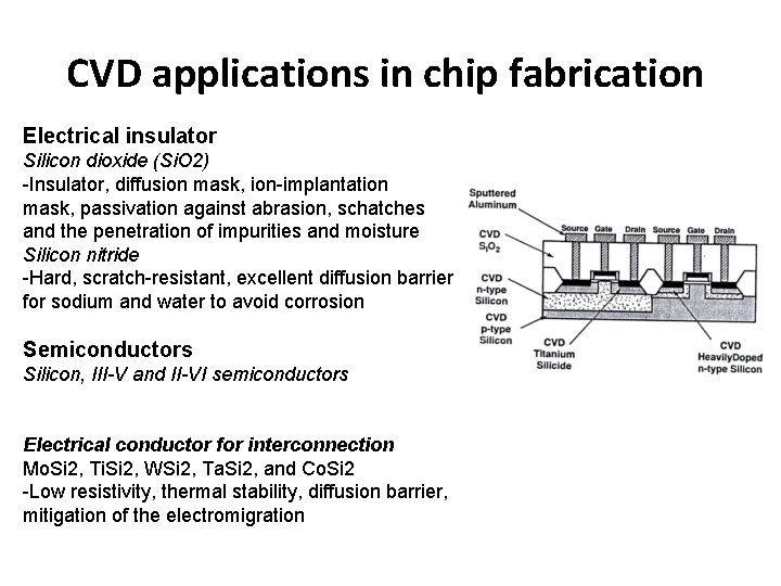
CVD applications in chip fabrication Electrical insulator Silicon dioxide (Si. O 2) -Insulator, diffusion mask, ion-implantation mask, passivation against abrasion, schatches and the penetration of impurities and moisture Silicon nitride -Hard, scratch-resistant, excellent diffusion barrier for sodium and water to avoid corrosion Semiconductors Silicon, III-V and II-VI semiconductors Electrical conductor for interconnection Mo. Si 2, Ti. Si 2, WSi 2, Ta. Si 2, and Co. Si 2 -Low resistivity, thermal stability, diffusion barrier, mitigation of the electromigration
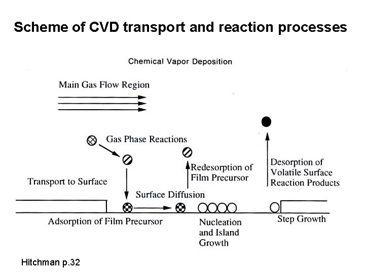
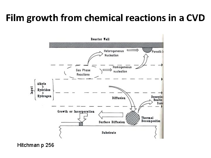
Scheme of CVD transport and reaction processes Hitchman p. 32
Film growth from chemical reactions in a CVD Hitchman p 256
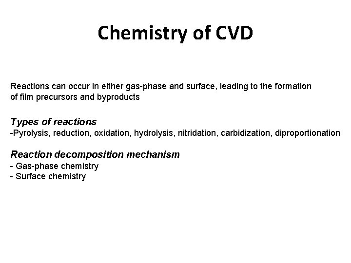
Chemistry of CVD Reactions can occur in either gas-phase and surface, leading to the formation of film precursors and byproducts Types of reactions -Pyrolysis, reduction, oxidation, hydrolysis, nitridation, carbidization, diproportionation Reaction decomposition mechanism - Gas-phase chemistry - Surface chemistry
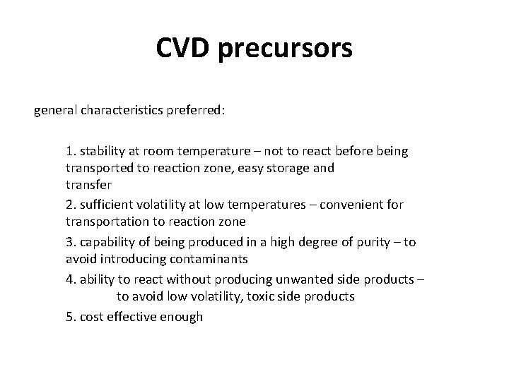
CVD precursors general characteristics preferred: 1. stability at room temperature – not to react before being transported to reaction zone, easy storage and transfer 2. sufficient volatility at low temperatures – convenient for transportation to reaction zone 3. capability of being produced in a high degree of purity – to avoid introducing contaminants 4. ability to react without producing unwanted side products – to avoid low volatility, toxic side products 5. cost effective enough
Common CVD precursors halides: {F, Cl, Br, I} + more electropositive elements {Al. Br 3, Al. Cl 3, BF 3, CCl 4, CF 4, Cr. Cl 2, Si. Cl 4, Ti. Cl 4, WF 6, Zr. Br 4, Zr. Cl 4…} metal-organics: (reactive, volatile, moisture sensitive, low decomposition temperatures, not restricted to metals) M {in IIa, IIb, IIIa, IVa, VIa} + one or more carbon (oxygen) atoms of an organic hydrocarbon groups (alkyls: -CH 3, C 2 H 5, …; aryls: -C 6 H 5, …; acetylacetonates: -OC 5 H 8 O-, …) (CH 3)3 Al, (C 2 H 5)2 B, (CH 3)2 Cd, (C 6 H 5)2 Be, Ca(C 5 H 8 O 2)2 … metal carbonyls: -(CO)- + transition metals with partially filled d-shell 3 d : Sc, Ti, V, Cr, Mn, Fe, Co, Ni 4 d : Y, Zr, Nb, Mo, Tc, Ru, Rh, Pd, Ag 5 d : Hf, Ta, W, Re, Os, Ir, Pt, Au mononuclear, M(CO)x : Cr(CO)6, Fe(CO)5, Ni(CO)4, W(CO)6 dinuclear, M 2(CO)x : Mn 2(CO)12, Fe 2(CO)9, Co 2(CO)8 polynuclear : Fe 3(CO)12, Co 4(CO)12 metal carbonyl complexes: Mn(CO)Cl, Co. NO(CO)3 hydrides: H 2 + {IIIa, IVa, VIa} As. H 3, B 2 H 6, Si. H 4, NH 3, …
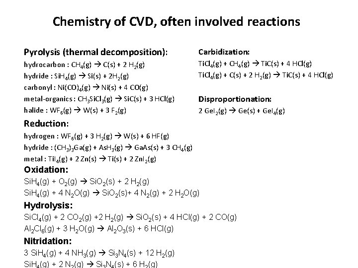
Chemistry of CVD, often involved reactions Pyrolysis (thermal decomposition): Carbidization: hydrocarbon : CH 4(g) C(s) + 2 H 2(g) hydride : Si. H 4(g) Si(s) + 2 H 2(g) carbonyl : Ni(CO)4(g) Ni(s) + 4 CO(g) metal-organics : CH 3 Si. Cl 3(g) Si. C(s) + 3 HCl(g) halide : WF 6(g) W(s) + 3 F 2(g) Ti. Cl 4(g) + CH 4(g) Ti. C(s) + 4 HCl(g) Ti. Cl 4(g) + C(s) + 2 H 2(g) Ti. C(s) + 4 HCl(g) Disproportionation: 2 Ge. I 2(g) Ge(s) + Ge. I 4(g) Reduction: hydrogen : WF 6(g) + 3 H 2(g) W(s) + 6 HF(g) hydride : (CH 3)3 Ga(g) + As. H 3(g) Ga. As(s) + 3 CH 4(g) metal : Ti. I 4(g) + 2 Zn(s) Ti(s) + 2 Zn. I 2(g) Oxidation: Si. H 4(g) + O 2(g) Si. O 2(s) + 2 H 2(g) Si. H 4(g) + 4 N 2 O(g) Si. O 2(s)+ 4 N 2(g) + 2 H 2 O(g) Hydrolysis: Si. Cl 4(g) + 2 CO 2(g) +2 H 2(g) Si. O 2(s) + 4 HCl(g) + 2 CO(g) Al 2 Cl 6(g) + 3 H 2 O(g) Al 2 O 3(s) + 6 HCl(g) Nitridation: 3 Si. H 4(g) + 4 NH 3(g) Si 3 N 4(s) + 12 H 2(g) Si. H (g) + 2 N (g) Si N (s) + 6 H (g)
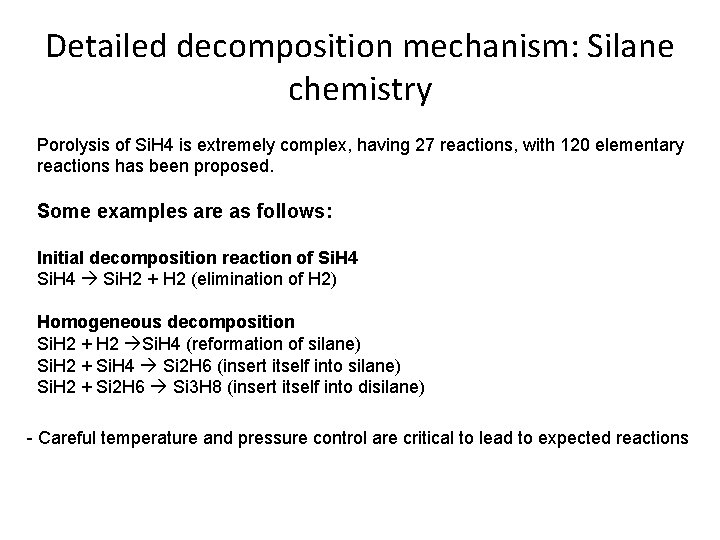
Detailed decomposition mechanism: Silane chemistry Porolysis of Si. H 4 is extremely complex, having 27 reactions, with 120 elementary reactions has been proposed. Some examples are as follows: Initial decomposition reaction of Si. H 4 Si. H 2 + H 2 (elimination of H 2) Homogeneous decomposition Si. H 2 + H 2 Si. H 4 (reformation of silane) Si. H 2 + Si. H 4 Si 2 H 6 (insert itself into silane) Si. H 2 + Si 2 H 6 Si 3 H 8 (insert itself into disilane) - Careful temperature and pressure control are critical to lead to expected reactions
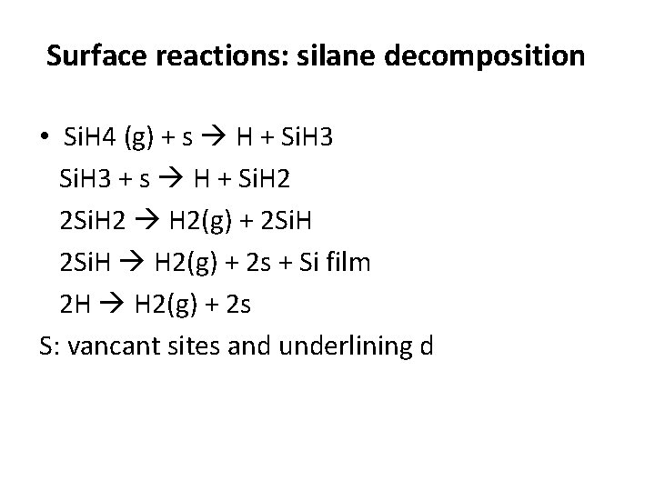
Surface reactions: silane decomposition • Si. H 4 (g) + s H + Si. H 3 + s H + Si. H 2 2 Si. H 2(g) + 2 Si. H H 2(g) + 2 s + Si film 2 H H 2(g) + 2 s S: vancant sites and underlining d
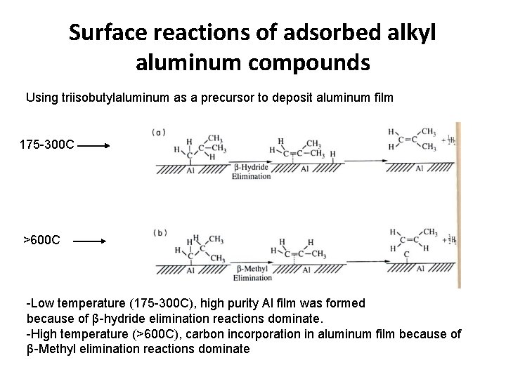
Surface reactions of adsorbed alkyl aluminum compounds Using triisobutylaluminum as a precursor to deposit aluminum film 175 -300 C >600 C -Low temperature (175 -300 C), high purity Al film was formed because of β-hydride elimination reactions dominate. -High temperature (>600 C), carbon incorporation in aluminum film because of β-Methyl elimination reactions dominate
An example: In-situ phosphorus-doped polycrystalline Si Precursors: Si. H 4+PH 3/N 2 Overall process: Si. H 4+x. PH 3/N 2 Si. Px + x. N 2 + (1. 5 x+2)H 2 Growth reactions k 4’ Si. H 4(a) Si(s) +2 H 2(a) k 3’ Si 2 H 6(a) 2 Si(s) + 3 H 2(a) k 2’ Si. H 2(a) Si(s) + H 2(a) Gas-phase reactions: k. R Si. H 4(g) Si. H 2(g) + H 2 (g) k. R k. D Si. H 4(g) + Si. H 2(g) Si 2 H 6(g) KD Adsorption equilibria ka. S Si. H 4(g) Si. H 4(a) kd. S ka. R Si. H 2(g) Si. H 2(a) kd. R ka. D Si 2 H 6(g) Si 2 H 6(a) ka. Pkd. D PH 3(g) PH 3(a) ka. Hkd. P H 2(g) H 2(a) Hietchman p 201 kd. H
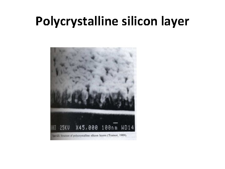
Polycrystalline silicon layer
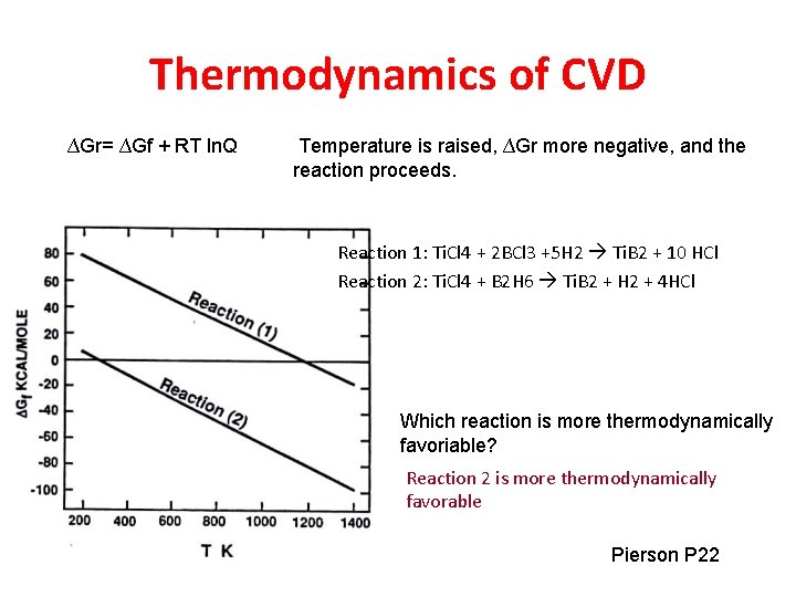
Thermodynamics of CVD ∆Gr= ∆Gf + RT ln. Q Temperature is raised, ∆Gr more negative, and the reaction proceeds. Reaction 1: Ti. Cl 4 + 2 BCl 3 +5 H 2 Ti. B 2 + 10 HCl Reaction 2: Ti. Cl 4 + B 2 H 6 Ti. B 2 + H 2 + 4 HCl Which reaction is more thermodynamically favoriable? Reaction 2 is more thermodynamically favorable Pierson P 22
Kinetics and Mass transport mechanism • Deposition sequence • Boundary layer • Rate determining steps
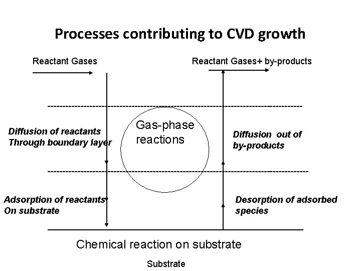
Processes contributing to CVD growth Reactant Gases Reactant Gases+ by-products ------------------------------------------Diffusion of reactants Through boundary layer Gas-phase reactions Diffusion out of by-products -------------------------------------------Adsorption of reactants On substrate Desorption of adsorbed species __________________________ Chemical reaction on substrate Substrate
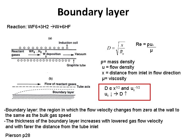
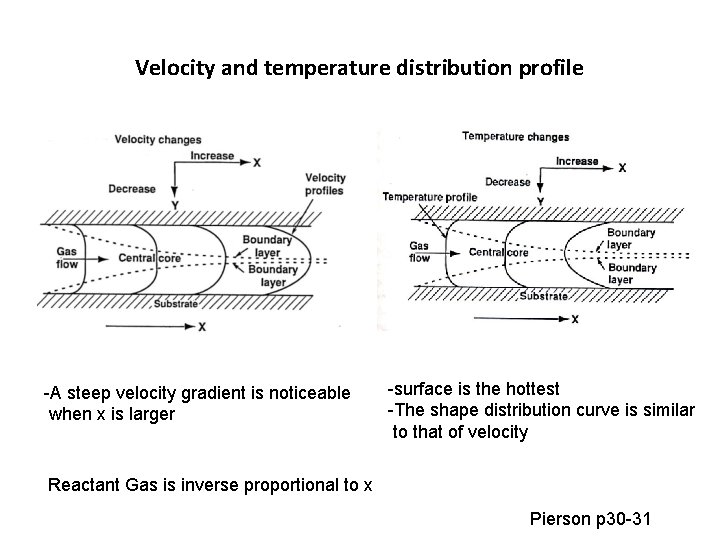
Boundary layer Reaction: WF 6+3 H 2 W+6 HF Re = ρux μ ρ= mass density u = flow density x = distance from inlet in flow direction μ= viscosity x D D α x 1/2 and ux-1/2 ux ↓ D -Boundary layer: the region in which the flow velocity changes from zero at the wall to the same as the bulk gas speed -The thickness of the boundary layer increases with lowered gas flow velocity and with farer the distance from the tube inlet Pierson p 28
Velocity and temperature distribution profile -A steep velocity gradient is noticeable when x is larger -surface is the hottest -The shape distribution curve is similar to that of velocity Reactant Gas is inverse proportional to x Pierson p 30 -31
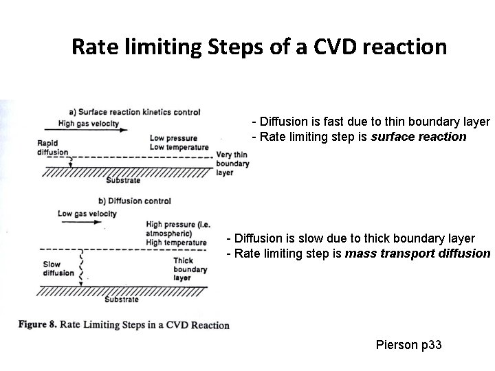
Rate limiting Steps of a CVD reaction - Diffusion is fast due to thin boundary layer - Rate limiting step is surface reaction - Diffusion is slow due to thick boundary layer - Rate limiting step is mass transport diffusion Pierson p 33
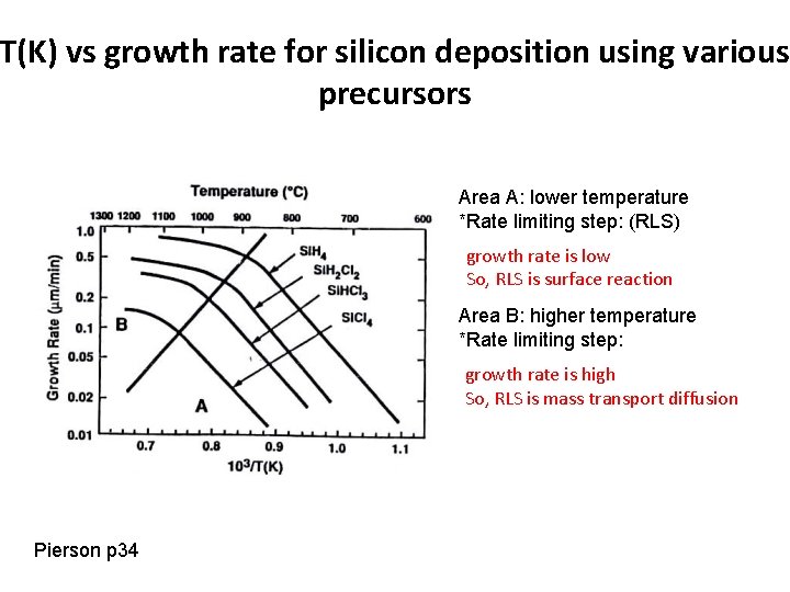
T(K) vs growth rate for silicon deposition using various precursors Area A: lower temperature *Rate limiting step: (RLS) growth rate is low So, RLS is surface reaction Area B: higher temperature *Rate limiting step: growth rate is high So, RLS is mass transport diffusion Pierson p 34
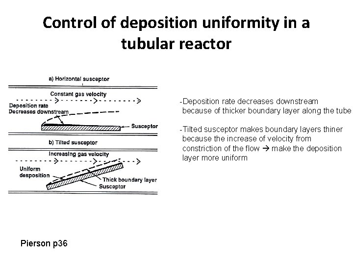
Control of deposition uniformity in a tubular reactor -Deposition rate decreases downstream because of thicker boundary layer along the tube -Tilted susceptor makes boundary layers thiner because the increase of velocity from constriction of the flow make the deposition layer more uniform Pierson p 36
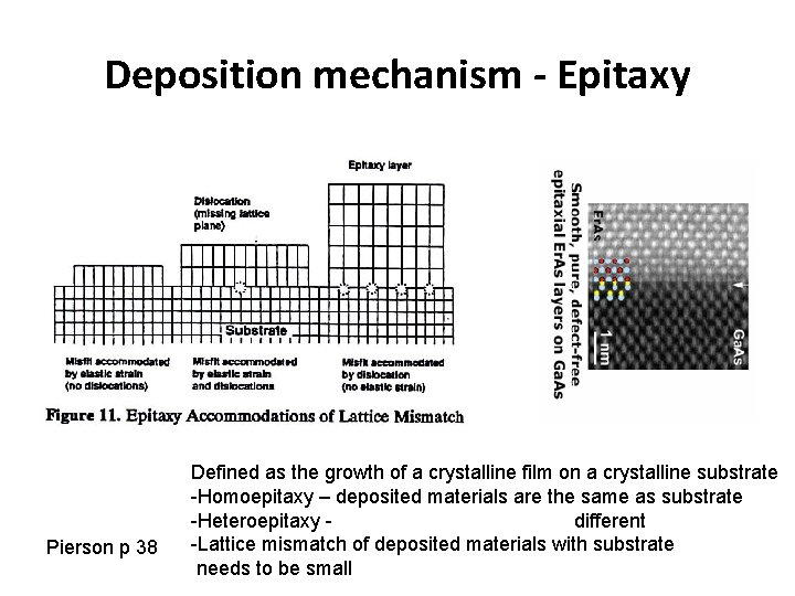
Deposition mechanism - Epitaxy Pierson p 38 Defined as the growth of a crystalline film on a crystalline substrate -Homoepitaxy – deposited materials are the same as substrate -Heteroepitaxy - different -Lattice mismatch of deposited materials with substrate needs to be small
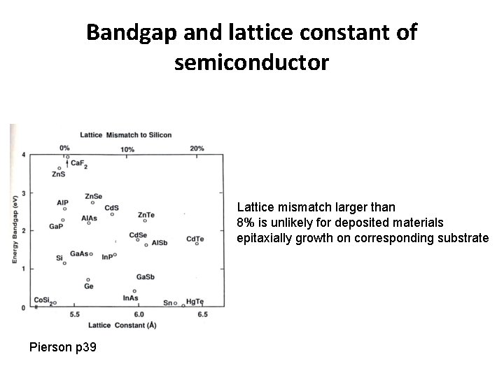
Bandgap and lattice constant of semiconductor -Lattice mismatch larger than 8% is unlikely for deposited materials epitaxially growth on corresponding substrate Pierson p 39
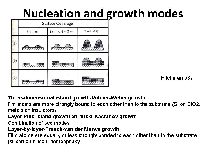
Nucleation and growth modes Hitchman p 37 Three-dimensional island growth-Volmer-Weber growth film atoms are more strongly bound to each other than to the substrate (Si on Si. O 2, metals on insulators) Layer-Plus-island growth-Stranski-Kastanov growth Combination of two modes Layer-by-layer-Franck-van der Merwe growth Film atoms are equally or less strongly bonded to each other than to the substrate (silicon on silicon, homoepitaxy
A Typical CVD Apparatus Reactant supply Chemical reactions in a CVD reactor Exhaust system
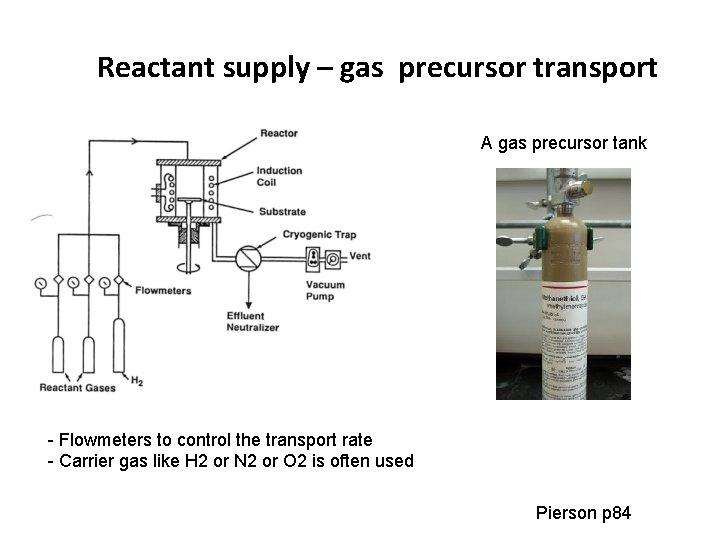
Reactant supply – gas precursor transport A gas precursor tank - Flowmeters to control the transport rate - Carrier gas like H 2 or N 2 or O 2 is often used Pierson p 84
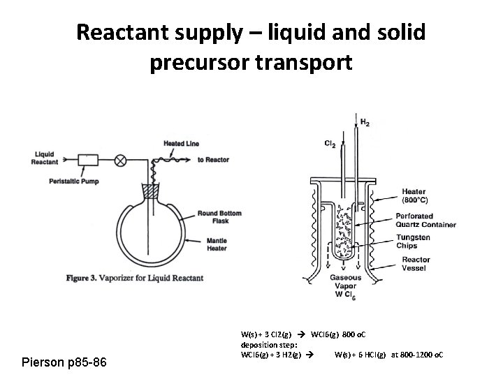
Reactant supply – liquid and solid precursor transport Pierson p 85 -86 W(s) + 3 Cl 2(g) WCl 6(g) 800 o. C deposition step: WCl 6(g) + 3 H 2(g) W(s) + 6 HCl(g) at 800 -1200 o. C
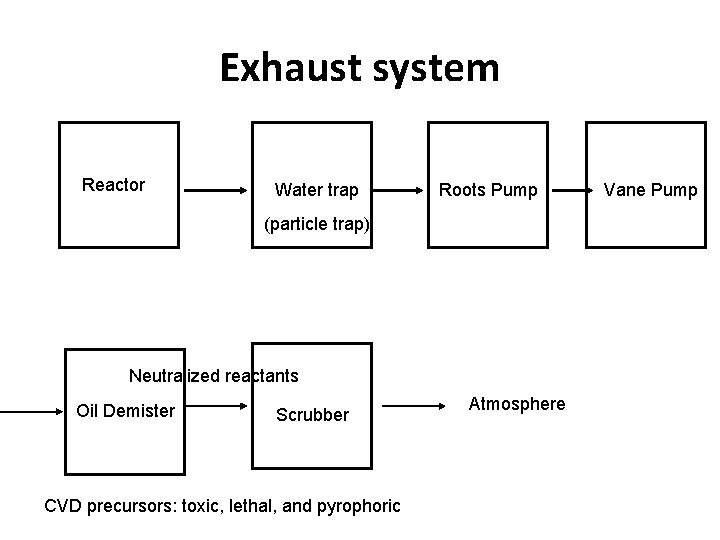
Exhaust system Reactor Water trap Roots Pump (particle trap) Neutralized reactants Oil Demister Scrubber CVD precursors: toxic, lethal, and pyrophoric Atmosphere Vane Pump