ELEC 5970 0016970 001Fall 2005 Special Topics in
- Slides: 43

ELEC 5970 -001/6970 -001(Fall 2005) Special Topics in Electrical Engineering Low-Power Design of Electronic Circuits Dynamic Power: Glitch Elimination Vishwani D. Agrawal James J. Danaher Professor Department of Electrical and Computer Engineering Auburn University http: //www. eng. auburn. edu/~vagrawal@eng. auburn. edu 9/20/05 ELEC 5970 -001/6970 -001 Lecture 8 1

Components of Power • Dynamic – Signal transitions • Logic activity • Glitches – Short-circuit • Static – Leakage 9/20/05 ELEC 5970 -001/6970 -001 Lecture 8 2

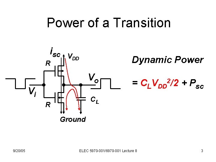
Power of a Transition isc R VDD Dynamic Power Vo Vi = CLVDD 2/2 + Psc CL R Ground 9/20/05 ELEC 5970 -001/6970 -001 Lecture 8 3

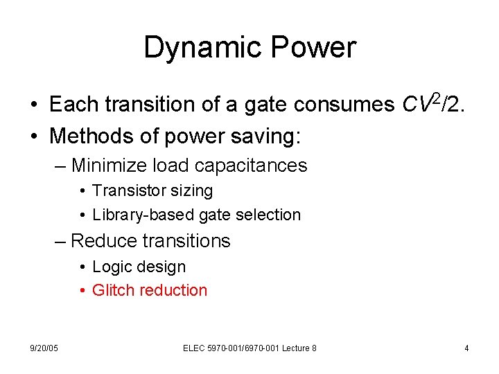
Dynamic Power • Each transition of a gate consumes CV 2/2. • Methods of power saving: – Minimize load capacitances • Transistor sizing • Library-based gate selection – Reduce transitions • Logic design • Glitch reduction 9/20/05 ELEC 5970 -001/6970 -001 Lecture 8 4

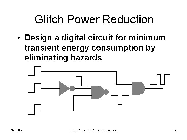
Glitch Power Reduction • Design a digital circuit for minimum transient energy consumption by eliminating hazards 9/20/05 ELEC 5970 -001/6970 -001 Lecture 8 5

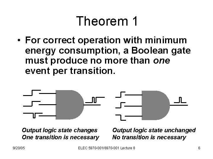
Theorem 1 • For correct operation with minimum energy consumption, a Boolean gate must produce no more than one event per transition. Output logic state changes One transition is necessary 9/20/05 Output logic state unchanged No transition is necessary ELEC 5970 -001/6970 -001 Lecture 8 6

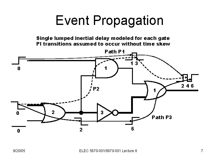
Event Propagation Single lumped inertial delay modeled for each gate PI transitions assumed to occur without time skew Path P 1 1 0 13 P 2 0 0 9/20/05 2 1 3 2 246 Path P 3 5 ELEC 5970 -001/6970 -001 Lecture 8 7

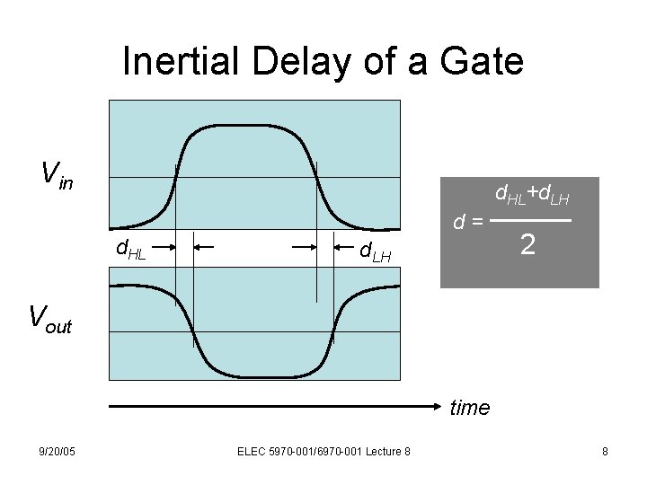
Inertial Delay of a Gate Vin d. HL+d. LH d. HL d = ──── 2 d. LH Vout time 9/20/05 ELEC 5970 -001/6970 -001 Lecture 8 8

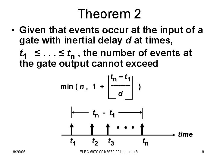
Theorem 2 • Given that events occur at the input of a gate with inertial delay d at times, t 1 ≤. . . ≤ tn , the number of events at the gate output cannot exceed tn – t 1 min ( n , 1 + -------d ) tn - t 1 9/20/05 t 2 t 3 ELEC 5970 -001/6970 -001 Lecture 8 tn time 9

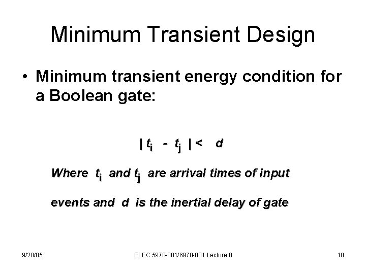
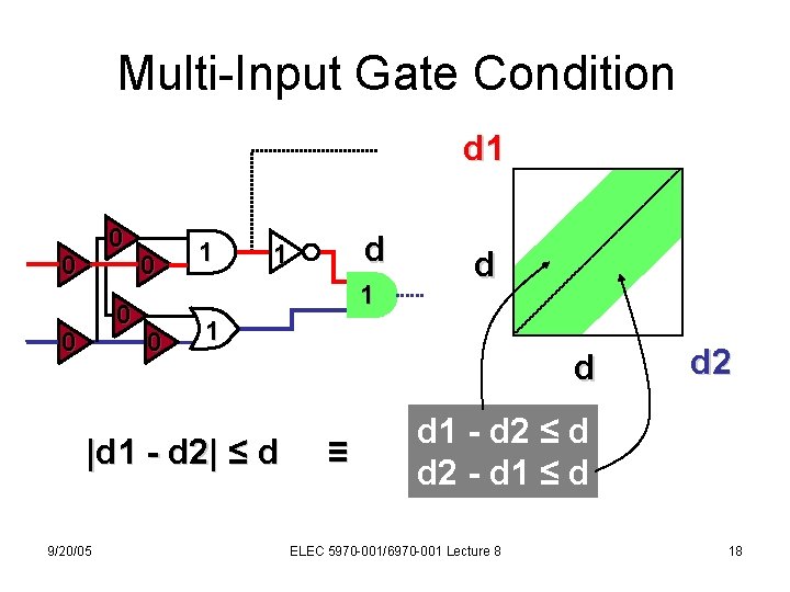
Minimum Transient Design • Minimum transient energy condition for a Boolean gate: | ti - tj | < d Where ti and tj are arrival times of input events and d is the inertial delay of gate 9/20/05 ELEC 5970 -001/6970 -001 Lecture 8 10

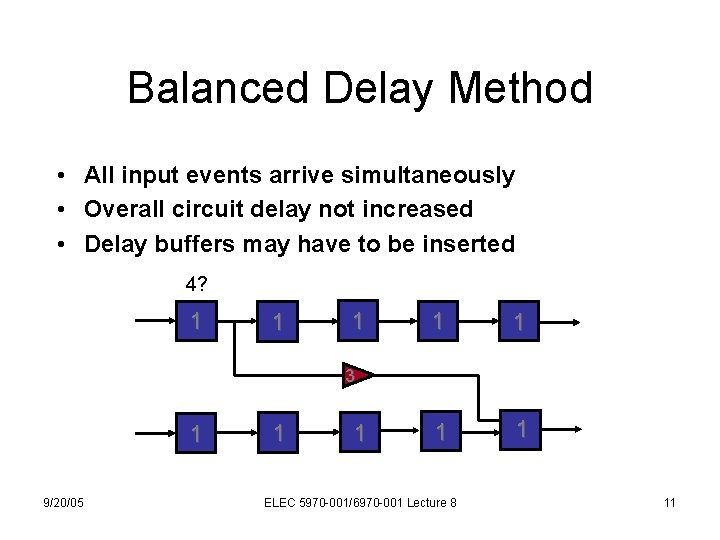
Balanced Delay Method • All input events arrive simultaneously • Overall circuit delay not increased • Delay buffers may have to be inserted 4? 1 1 1 1 3 1 9/20/05 1 1 ELEC 5970 -001/6970 -001 Lecture 8 11

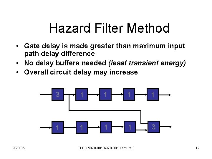
Hazard Filter Method • Gate delay is made greater than maximum input path delay difference • No delay buffers needed (least transient energy) • Overall circuit delay may increase 9/20/05 3 1 1 1 1 3 ELEC 5970 -001/6970 -001 Lecture 8 12

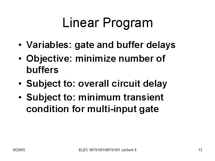
Linear Program • Variables: gate and buffer delays • Objective: minimize number of buffers • Subject to: overall circuit delay • Subject to: minimum transient condition for multi-input gate 9/20/05 ELEC 5970 -001/6970 -001 Lecture 8 13

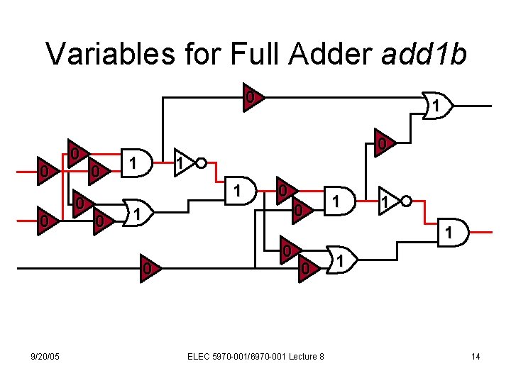
Variables for Full Adder add 1 b 0 0 0 0 1 1 1 0 9/20/05 1 0 0 1 1 1 0 ELEC 5970 -001/6970 -001 Lecture 8 1 14

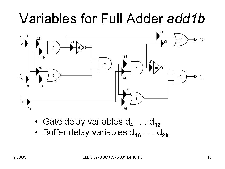
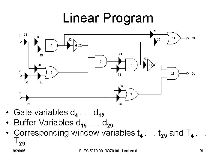
Variables for Full Adder add 1 b • Gate delay variables d 4. . . d 12 • Buffer delay variables d 15. . . d 29 9/20/05 ELEC 5970 -001/6970 -001 Lecture 8 15

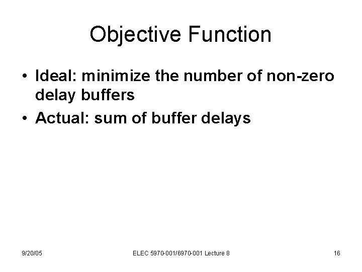
Objective Function • Ideal: minimize the number of non-zero delay buffers • Actual: sum of buffer delays 9/20/05 ELEC 5970 -001/6970 -001 Lecture 8 16

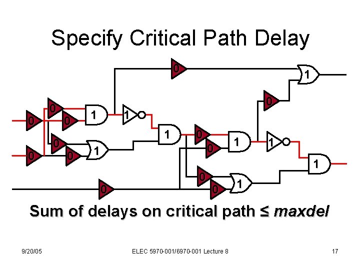
Specify Critical Path Delay 0 0 0 0 1 1 1 0 1 Sum of delays on critical path ≤ maxdel 9/20/05 ELEC 5970 -001/6970 -001 Lecture 8 17

Multi-Input Gate Condition d 1 0 0 0 1 1 |d 1 - d 2| ≤ d 9/20/05 d 1 d d ≡ d 2 d 1 - d 2 ≤ d d 2 - d 1 ≤ d ELEC 5970 -001/6970 -001 Lecture 8 18

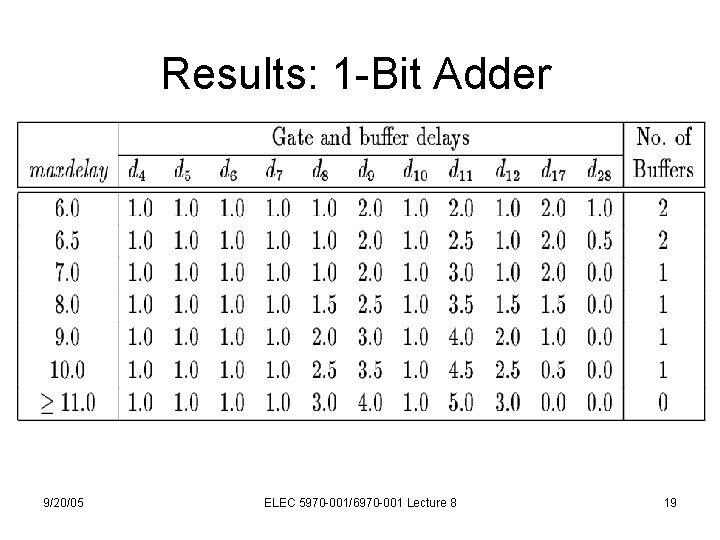
Results: 1 -Bit Adder 9/20/05 ELEC 5970 -001/6970 -001 Lecture 8 19

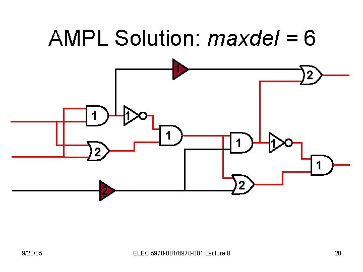
AMPL Solution: maxdel = 6 1 1 2 1 1 1 2 2 9/20/05 2 ELEC 5970 -001/6970 -001 Lecture 8 20

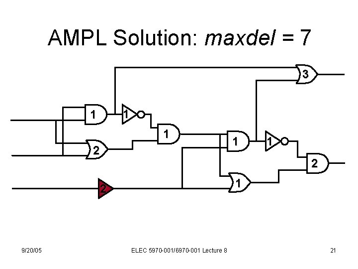
AMPL Solution: maxdel = 7 3 1 1 1 2 1 2 9/20/05 1 ELEC 5970 -001/6970 -001 Lecture 8 21

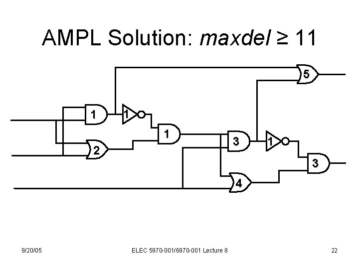
AMPL Solution: maxdel ≥ 11 5 1 1 1 2 3 1 3 4 9/20/05 ELEC 5970 -001/6970 -001 Lecture 8 22

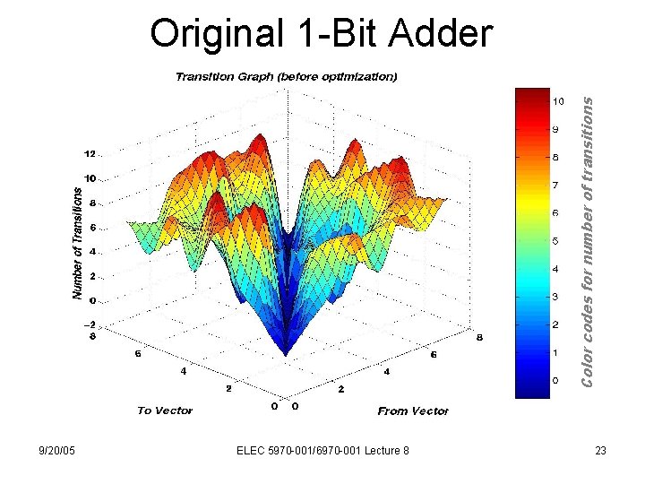
Color codes for number of transitions Original 1 -Bit Adder 9/20/05 ELEC 5970 -001/6970 -001 Lecture 8 23

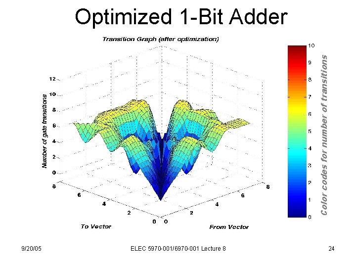
Color codes for number of transitions Optimized 1 -Bit Adder 9/20/05 ELEC 5970 -001/6970 -001 Lecture 8 24

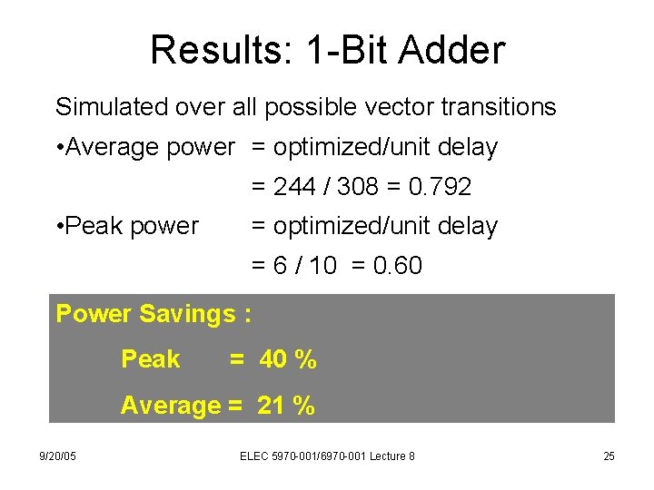
Results: 1 -Bit Adder Simulated over all possible vector transitions • Average power = optimized/unit delay = 244 / 308 = 0. 792 • Peak power = optimized/unit delay = 6 / 10 = 0. 60 Power Savings : Peak = 40 % Average = 21 % 9/20/05 ELEC 5970 -001/6970 -001 Lecture 8 25

References • E. Jacobs and M. Berkelaar, “Using Gate Sizing to Reduce Glitch Power, ” Proc. Pro. RISC/IEEE Workshop on Circuits, Systems and Signal Processing, Nov. 1996, pp. 183 -188; also Int. Workshop on Logic Synthesis, May 1997. • V. D. Agrawal, “Low-Power Design by Hazard Filtering, ” Proc. 10 th Int. Conf. VLSI Design, Jan. 1997, pp. 193 -197. • V. D. Agrawal, M. L. Bushnell, G. Parthasarathy, and R. Ramadoss, “Digital Circuit Design for Minimum Transient Energy and a Linear Programming Method, ” Proc. 12 th Int. Conf. VLSI Design, Jan. 1999, pp. 434 -439. • Last two papers are available at website http: //www. eng. auburn. edu/~vagrawal 9/20/05 ELEC 5970 -001/6970 -001 Lecture 8 26

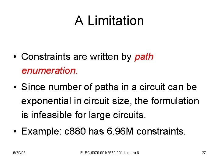
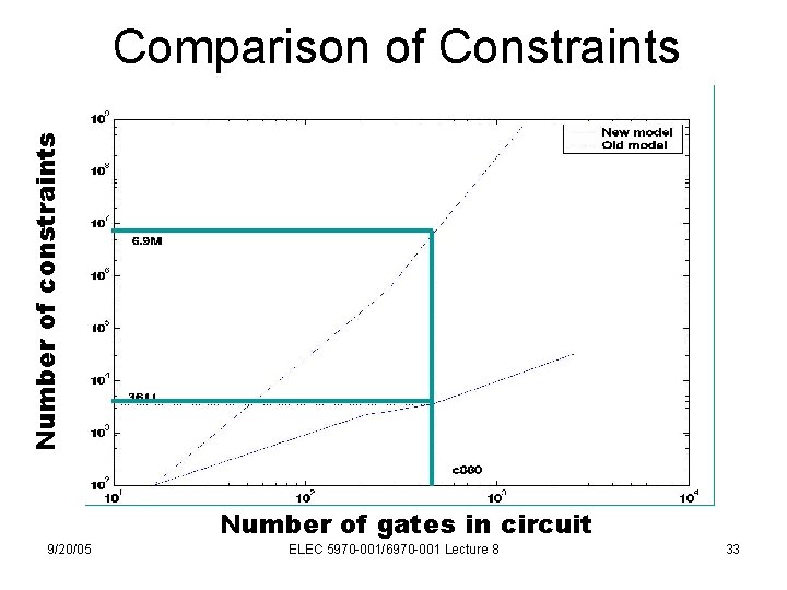
A Limitation • Constraints are written by path enumeration. • Since number of paths in a circuit can be exponential in circuit size, the formulation is infeasible for large circuits. • Example: c 880 has 6. 96 M constraints. 9/20/05 ELEC 5970 -001/6970 -001 Lecture 8 27

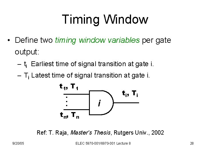
Timing Window • Define two timing window variables per gate output: – ti Earliest time of signal transition at gate i. – Ti Latest time of signal transition at gate i. t 1, T 1. . . i t i, T i t n , Tn Ref: T. Raja, Master’s Thesis, Rutgers Univ. , 2002 9/20/05 ELEC 5970 -001/6970 -001 Lecture 8 28

Linear Program • Gate variables d 4. . . d 12 • Buffer Variables d 15. . . d 29 • Corresponding window variables t 4. . . t 29 and T 4. . . T 29. 9/20/05 ELEC 5970 -001/6970 -001 Lecture 8 29

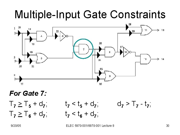
Multiple-Input Gate Constraints For Gate 7: T 7 > T 5 + d 7; T 7 > T 6 + d 7; 9/20/05 t 7 < t 5 + d 7; t 7 < t 6 + d 7; ELEC 5970 -001/6970 -001 Lecture 8 d 7 > T 7 - t 7; 30

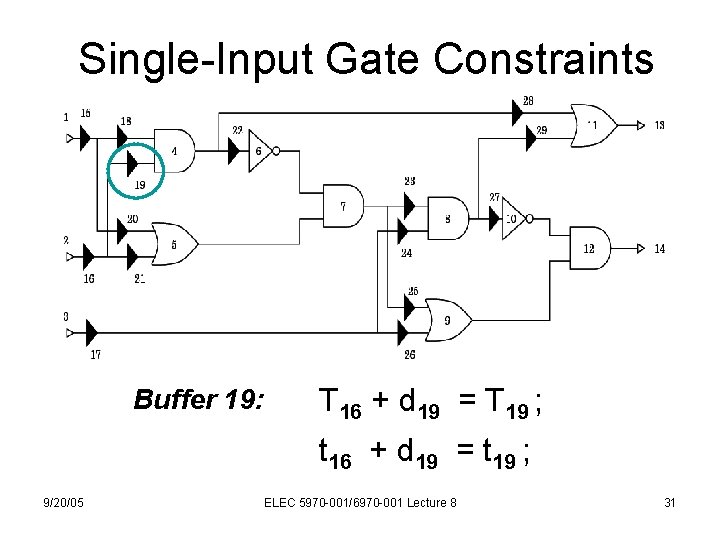
Single-Input Gate Constraints Buffer 19: T 16 + d 19 = T 19 ; t 16 + d 19 = t 19 ; 9/20/05 ELEC 5970 -001/6970 -001 Lecture 8 31

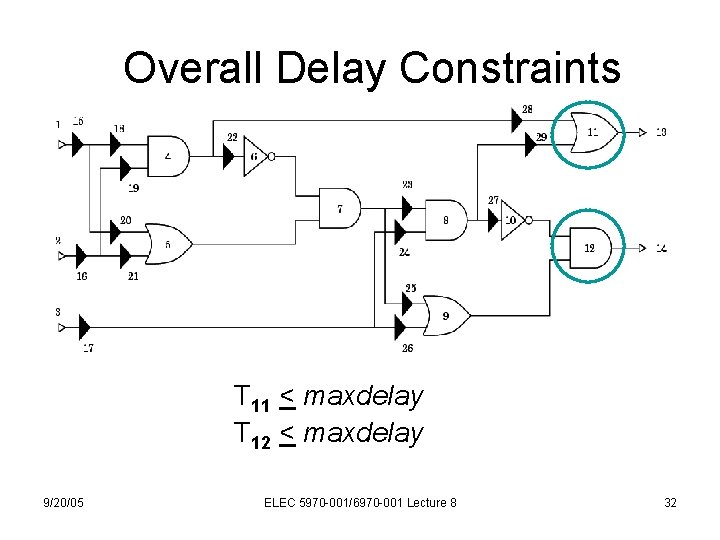
Overall Delay Constraints T 11 < maxdelay T 12 < maxdelay 9/20/05 ELEC 5970 -001/6970 -001 Lecture 8 32

Number of constraints Comparison of Constraints Number of gates in circuit 9/20/05 ELEC 5970 -001/6970 -001 Lecture 8 33

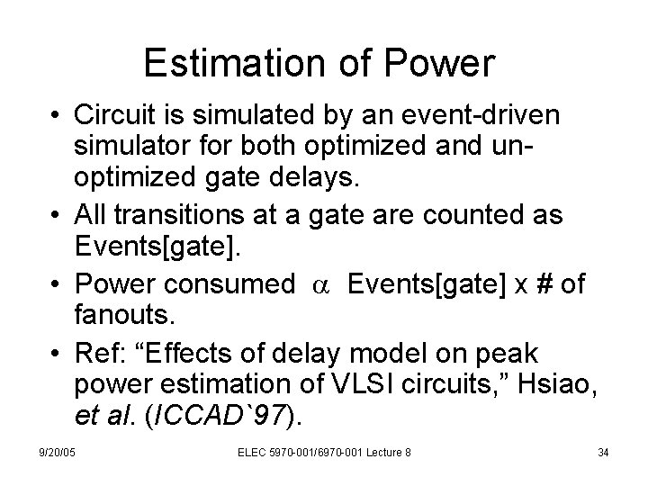
Estimation of Power • Circuit is simulated by an event-driven simulator for both optimized and unoptimized gate delays. • All transitions at a gate are counted as Events[gate]. • Power consumed Events[gate] x # of fanouts. • Ref: “Effects of delay model on peak power estimation of VLSI circuits, ” Hsiao, et al. (ICCAD`97). 9/20/05 ELEC 5970 -001/6970 -001 Lecture 8 34

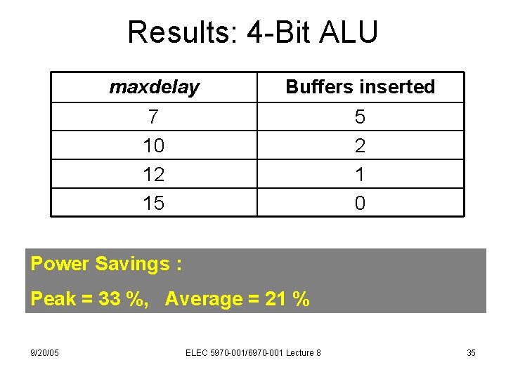
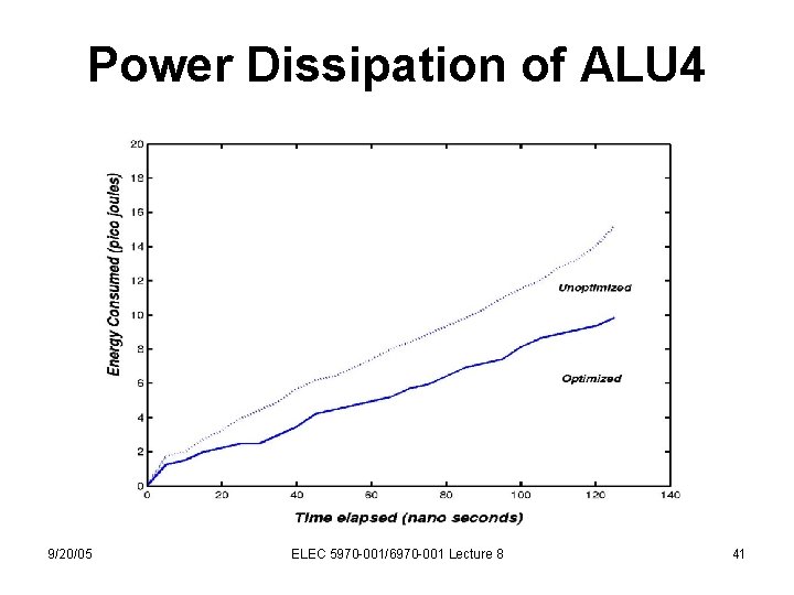
Results: 4 -Bit ALU maxdelay Buffers inserted 7 10 12 15 5 2 1 0 Power Savings : Peak = 33 %, Average = 21 % 9/20/05 ELEC 5970 -001/6970 -001 Lecture 8 35

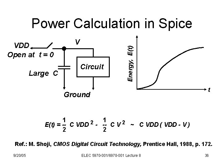
VDD Open at t = 0 Large C V Circuit Energy, E(t) Power Calculation in Spice Ground t 1 1 2 E(t) = -- C VDD - -- C V 2 ~ C VDD ( VDD - V ) 2 2 Ref. : M. Shoji, CMOS Digital Circuit Technology, Prentice Hall, 1988, p. 172. 9/20/05 ELEC 5970 -001/6970 -001 Lecture 8 36

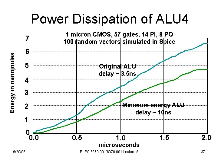
Power Dissipation of ALU 4 Energy in nanojoules 7 1 micron CMOS, 57 gates, 14 PI, 8 PO 100 random vectors simulated in Spice 6 5 Original ALU delay ~ 3. 5 ns 4 3 Minimum energy ALU delay ~ 10 ns 2 1 0 0. 5 1. 0 1. 5 2. 0 microseconds 9/20/05 ELEC 5970 -001/6970 -001 Lecture 8 37

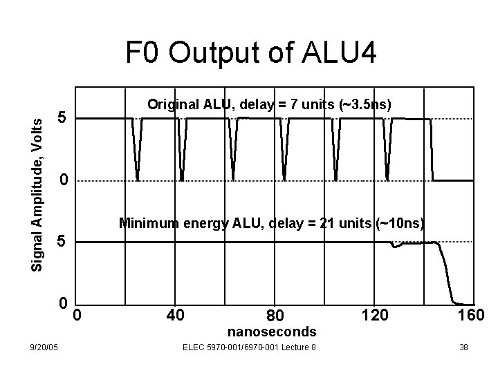
Signal Amplitude, Volts F 0 Output of ALU 4 Original ALU, delay = 7 units (~3. 5 ns) 5 0 Minimum energy ALU, delay = 21 units (~10 ns) 5 0 0 40 80 120 160 nanoseconds 9/20/05 ELEC 5970 -001/6970 -001 Lecture 8 38

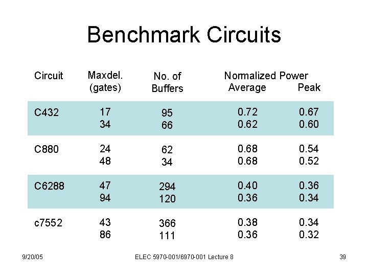
Benchmark Circuits Circuit Maxdel. (gates) No. of Buffers C 432 17 34 95 66 0. 72 0. 67 0. 60 C 880 24 48 62 34 0. 68 0. 54 0. 52 C 6288 47 94 294 120 0. 40 0. 36 0. 34 c 7552 43 86 366 111 0. 38 0. 36 0. 34 0. 32 9/20/05 Normalized Power Average Peak ELEC 5970 -001/6970 -001 Lecture 8 39

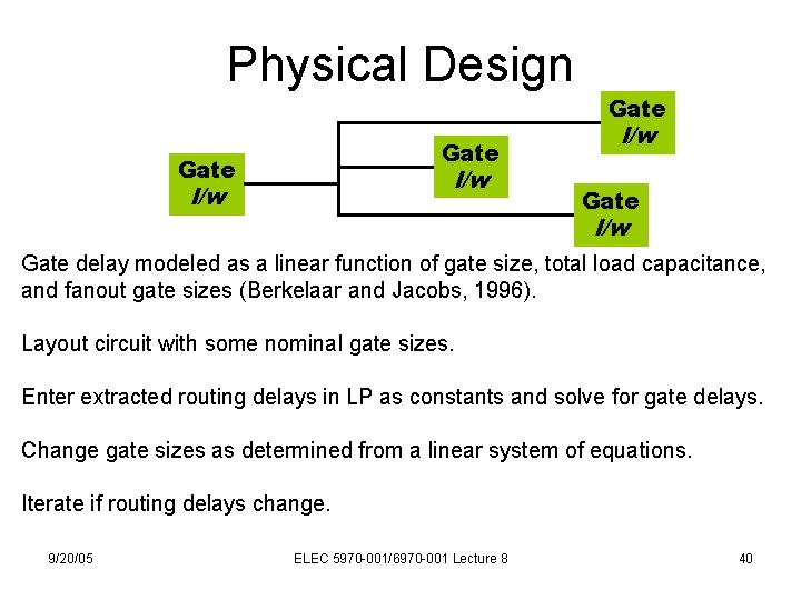
Physical Design Gate l/w l/w Gate delay modeled as a linear function of gate size, total load capacitance, and fanout gate sizes (Berkelaar and Jacobs, 1996). Layout circuit with some nominal gate sizes. Enter extracted routing delays in LP as constants and solve for gate delays. Change gate sizes as determined from a linear system of equations. Iterate if routing delays change. 9/20/05 ELEC 5970 -001/6970 -001 Lecture 8 40

Power Dissipation of ALU 4 9/20/05 ELEC 5970 -001/6970 -001 Lecture 8 41

References • R. Fourer, D. M. Gay and B. W. Kernighan, AMPL: A Modeling Language for Mathematical Programming, South San Francisco: The Scientific Press, 1993. • M. Berkelaar and E. Jacobs, “Using Gate Sizing to Reduce Glitch Power, ” Proc. Pro. RISC Workshop, Mierlo, The Netherlands, Nov. 1996, pp. 183 -188. • V. D. Agrawal, “Low Power Design by Hazard Filtering, ” Proc. 10 th Int’l Conf. VLSI Design, Jan. 1997, pp. 193 -197. • V. D. Agrawal, M. L. Bushnell, G. Parthasarathy and R. Ramadoss, “Digital Circuit Design for Minimum Transient Energy and Linear Programming Method, ” Proc. 12 th Int’l Conf. VLSI Design, Jan. 1999, pp. 434 -439. • M. Hsiao, E. M. Rudnick and J. H. Patel, “Effects of Delay Model in Peak Power Estimation of VLSI Circuits, ” Proc. ICCAD, Nov. 1997, pp. 45 -51. • T. Raja, A Reduced Constraint Set Linear Program for Low Power Design of Digital Circuits, Master’s Thesis, Rutgers Univ. , New Jersey, 2002. 9/20/05 ELEC 5970 -001/6970 -001 Lecture 8 42

Conclusion • Glitch-free design through LP: constraint-set is linear in the size of the circuit. • LP solution: – Eliminates glitches at all gate outputs, – Holds I/O delay within specification, and – Combines path-balancing and hazard-filtering to minimize the number of delay buffers. • Linear constraint set LP produces results exactly identical to the LP requiring exponential constraint-set. • Results show peak power savings up to 68% and average power savings up to 64%. 9/20/05 ELEC 5970 -001/6970 -001 Lecture 8 43