ELEC 5970 0016970 001Fall 2005 Special Topics in
![i(t) = C dv(t)/dt = [V – v(t)] /R dv(t) V – v(t) ─── i(t) = C dv(t)/dt = [V – v(t)] /R dv(t) V – v(t) ───](https://slidetodoc.com/presentation_image_h2/f5bdca0c21e869fb1a613c76e3802697/image-6.jpg)
![v(t) = i(t) 8/23 -25/05 = -t V [1 – exp( ── )] RC v(t) = i(t) 8/23 -25/05 = -t V [1 – exp( ── )] RC](https://slidetodoc.com/presentation_image_h2/f5bdca0c21e869fb1a613c76e3802697/image-7.jpg)
![isc, Rise Time and Capacitance Isc(t) = 8/23 -25/05 -t VDD[1 - exp(─────)] vo(t) isc, Rise Time and Capacitance Isc(t) = 8/23 -25/05 -t VDD[1 - exp(─────)] vo(t)](https://slidetodoc.com/presentation_image_h2/f5bdca0c21e869fb1a613c76e3802697/image-20.jpg)
- Slides: 35

ELEC 5970 -001/6970 -001(Fall 2005) Special Topics in Electrical Engineering Low-Power Design of Electronic Circuits Power Consumption in a CMOS Circuit Vishwani D. Agrawal James J. Danaher Professor Department of Electrical and Computer Engineering Auburn University http: //www. eng. auburn. edu/~vagrawal@eng. auburn. edu 8/23 -25/05 ELEC 5970 -001/6970 -001 Lecture 2 1

Class Projects • • • Study of leakage dynamic power in nanometer devices Low leakage technologies Charge recovery and adiabatic switching circuits Simulation-based power estimation tool Transistor-sizing for low power Logic and flip-flop design for low power Low power clock distribution Low power arithmetic circuits Low power memory design Benchmarking of low power microprocessors Low power system design 8/23 -25/05 ELEC 5970 -001/6970 -001 Lecture 2 2

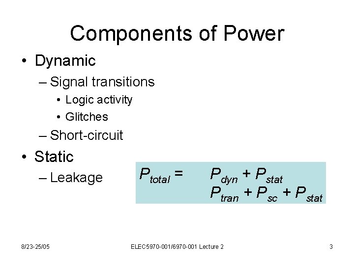
Components of Power • Dynamic – Signal transitions • Logic activity • Glitches – Short-circuit • Static – Leakage 8/23 -25/05 Ptotal = Pdyn + Pstat Ptran + Psc + Pstat ELEC 5970 -001/6970 -001 Lecture 2 3

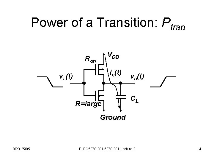
Power of a Transition: Ptran VDD Ron ic(t) vi (t) R=large vo(t) CL Ground 8/23 -25/05 ELEC 5970 -001/6970 -001 Lecture 2 4

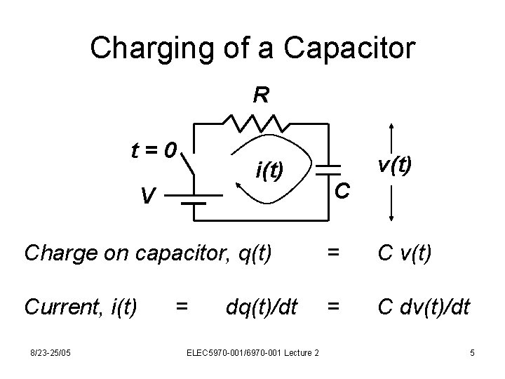
Charging of a Capacitor R t=0 i(t) V v(t) C Charge on capacitor, q(t) = C v(t) Current, i(t) = C dv(t)/dt 8/23 -25/05 = dq(t)/dt ELEC 5970 -001/6970 -001 Lecture 2 5
![it C dvtdt V vt R dvt V vt i(t) = C dv(t)/dt = [V – v(t)] /R dv(t) V – v(t) ───](https://slidetodoc.com/presentation_image_h2/f5bdca0c21e869fb1a613c76e3802697/image-6.jpg)
i(t) = C dv(t)/dt = [V – v(t)] /R dv(t) V – v(t) ─── = ───── dt RC dv(t) dt ∫ ───── = ∫───── V – v(t) RC -t ln [V – v(t)] = ── + A RC Initial condition, t = 0, v(t) = 0 → A = ln V -t v(t) = V [1 – exp(───)] RC 8/23 -25/05 ELEC 5970 -001/6970 -001 Lecture 2 6
![vt it 823 2505 t V 1 exp RC v(t) = i(t) 8/23 -25/05 = -t V [1 – exp( ── )] RC](https://slidetodoc.com/presentation_image_h2/f5bdca0c21e869fb1a613c76e3802697/image-7.jpg)
v(t) = i(t) 8/23 -25/05 = -t V [1 – exp( ── )] RC dv(t) C ─── dt = V -t ── exp( ── ) R RC ELEC 5970 -001/6970 -001 Lecture 2 7

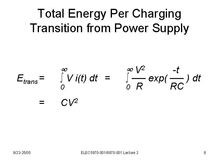
Total Energy Per Charging Transition from Power Supply Etrans = = 8/23 -25/05 ∞ ∫ V i(t) dt = 0 ∞ V 2 -t ∫ ── exp( ── ) dt 0 R RC CV 2 ELEC 5970 -001/6970 -001 Lecture 2 8

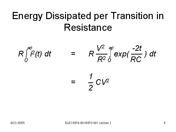
Energy Dissipated per Transition in Resistance ∞ 2 R ∫ i (t) dt 0 8/23 -25/05 = V 2 ∞ -2 t R ── ∫ exp( ── ) dt R 2 0 RC = 1 ─ CV 2 2 ELEC 5970 -001/6970 -001 Lecture 2 9

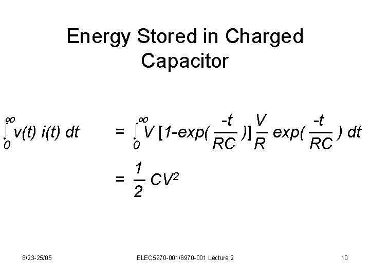
Energy Stored in Charged Capacitor ∞ ∫ v(t) i(t) dt 0 8/23 -25/05 ∞ -t V -t = ∫ V [1 -exp( ── )] ─ exp( ── ) dt 0 RC R RC 1 = ─ CV 2 2 ELEC 5970 -001/6970 -001 Lecture 2 10

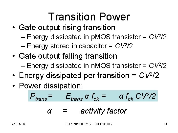
Transition Power • Gate output rising transition – Energy dissipated in p. MOS transistor = CV 2/2 – Energy stored in capacitor = CV 2/2 • Gate output falling transition – Energy dissipated in n. MOS transistor = CV 2/2 • Energy dissipated per transition = CV 2/2 • Power dissipation: Ptrans = Etrans α fck = α fck CV 2/2 α 8/23 -25/05 = activity factor ELEC 5970 -001/6970 -001 Lecture 2 11

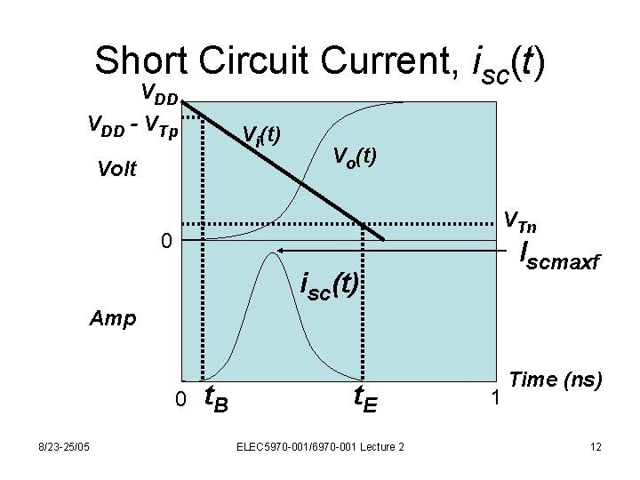
Short Circuit Current, isc(t) VDD - VTp Vi(t) Volt Vo(t) VTn 0 Iscmaxf isc(t) Amp 0 8/23 -25/05 t. B t. E ELEC 5970 -001/6970 -001 Lecture 2 1 Time (ns) 12

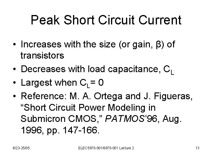
Peak Short Circuit Current • Increases with the size (or gain, β) of transistors • Decreases with load capacitance, CL • Largest when CL= 0 • Reference: M. A. Ortega and J. Figueras, “Short Circuit Power Modeling in Submicron CMOS, ” PATMOS’ 96, Aug. 1996, pp. 147 -166. 8/23 -25/05 ELEC 5970 -001/6970 -001 Lecture 2 13

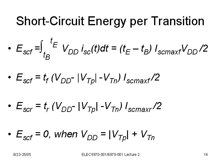
Short-Circuit Energy per Transition • Escf =∫ t. E t. B VDD isc(t)dt = (t. E – t. B) Iscmaxf. VDD /2 • Escf = tf (VDD- |VTp| -VTn) Iscmaxf /2 • Escr = tr (VDD- |VTp| -VTn) Iscmaxr /2 • Escf = 0, when VDD = |VTp| + VTn 8/23 -25/05 ELEC 5970 -001/6970 -001 Lecture 2 14

Short-Circuit Energy • Increases with rise and fall times of input • Decreases for larger output load capacitance • Decreases and eventually becomes zero when VDD is scaled down but the threshold voltages are not scaled down 8/23 -25/05 ELEC 5970 -001/6970 -001 Lecture 2 15

Short-Circuit Power Calculation • Assume equal rise and fall times • Model input-output capacitive coupling (Miller capacitance) • Use a spice model for transistors – T. Sakurai and A. Newton, “Alpha-power Law MOSFET model and Its Application to a CMOS Inverter, ” IEEE J. Solid State Circuits, vol. 25, April 1990, pp. 584 -594. 8/23 -25/05 ELEC 5970 -001/6970 -001 Lecture 2 16

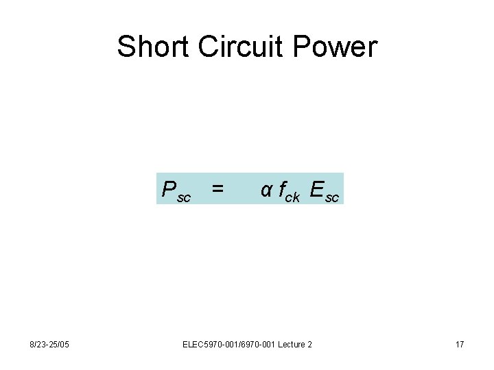
Short Circuit Power Psc = 8/23 -25/05 α fck Esc ELEC 5970 -001/6970 -001 Lecture 2 17

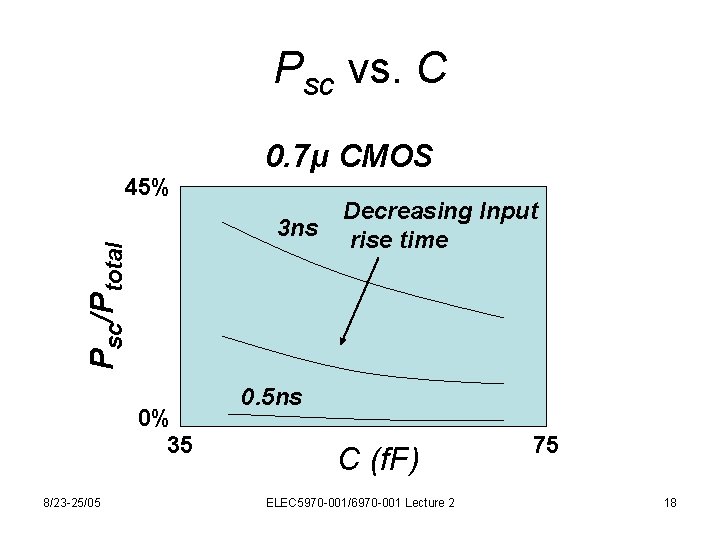
Psc vs. C 45% 0. 7μ CMOS Psc/Ptotal 3 ns 0% 35 8/23 -25/05 Decreasing Input rise time 0. 5 ns C (f. F) ELEC 5970 -001/6970 -001 Lecture 2 75 18

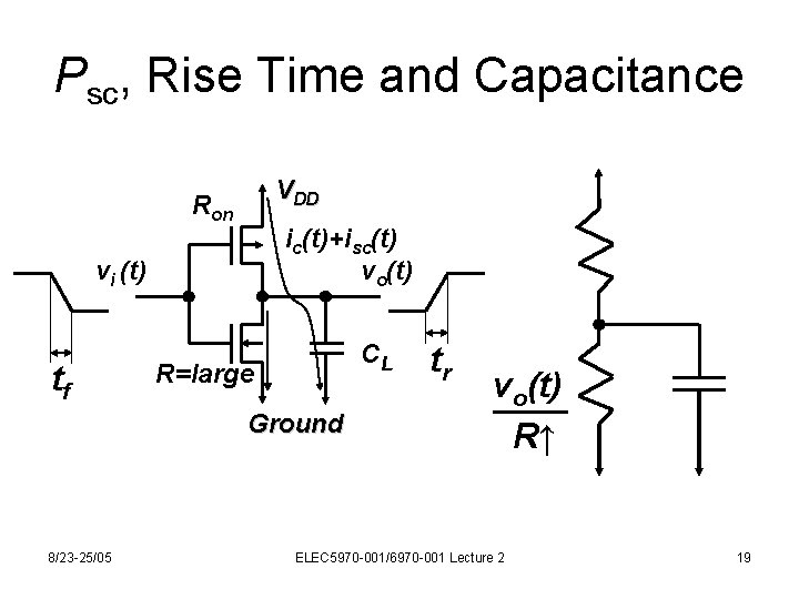
Psc, Rise Time and Capacitance VDD Ron ic(t)+isc(t) vo(t) vi (t) tf CL R=large Ground 8/23 -25/05 tr vo(t) ─── R↑ ELEC 5970 -001/6970 -001 Lecture 2 19
![isc Rise Time and Capacitance Isct 823 2505 t VDD1 exp vot isc, Rise Time and Capacitance Isc(t) = 8/23 -25/05 -t VDD[1 - exp(─────)] vo(t)](https://slidetodoc.com/presentation_image_h2/f5bdca0c21e869fb1a613c76e3802697/image-20.jpg)
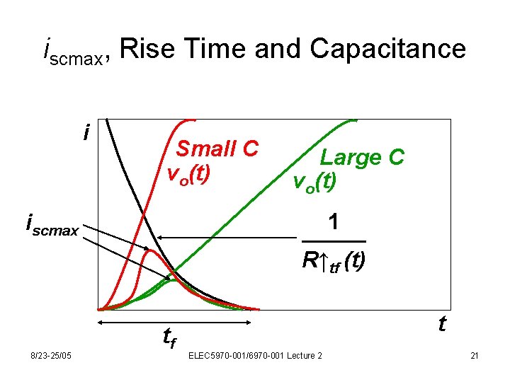
isc, Rise Time and Capacitance Isc(t) = 8/23 -25/05 -t VDD[1 - exp(─────)] vo(t) R↓tf (t)C ──── = ─────── R↑tf (t) ELEC 5970 -001/6970 -001 Lecture 2 20

iscmax, Rise Time and Capacitance i Small C vo(t) 1 ──── R↑tf (t) iscmax 8/23 -25/05 Large C vo(t) tf t ELEC 5970 -001/6970 -001 Lecture 2 21

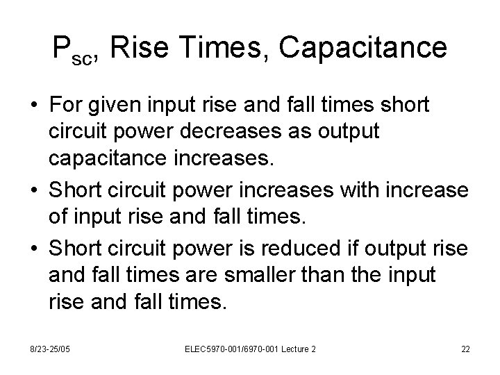
Psc, Rise Times, Capacitance • For given input rise and fall times short circuit power decreases as output capacitance increases. • Short circuit power increases with increase of input rise and fall times. • Short circuit power is reduced if output rise and fall times are smaller than the input rise and fall times. 8/23 -25/05 ELEC 5970 -001/6970 -001 Lecture 2 22

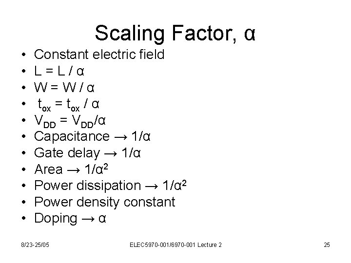
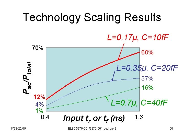
Technology Scaling • Scale down by factors of 2 and 4, i. e. , model 0. 7, 0. 35 and 0. 17 micron technologies • Constant electric field assumed • Capacitance scaled down by the technology scale down factor 8/23 -25/05 ELEC 5970 -001/6970 -001 Lecture 2 23

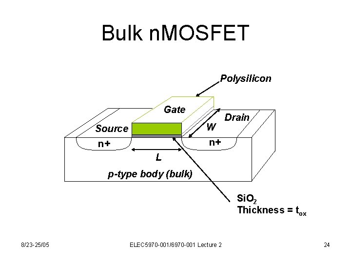
Bulk n. MOSFET Polysilicon Gate W Source Drain n+ n+ L p-type body (bulk) Si. O 2 Thickness = tox 8/23 -25/05 ELEC 5970 -001/6970 -001 Lecture 2 24

Scaling Factor, α • • • Constant electric field L=L/α W=W/α tox = tox / α VDD = VDD/α Capacitance → 1/α Gate delay → 1/α Area → 1/α 2 Power dissipation → 1/α 2 Power density constant Doping → α 8/23 -25/05 ELEC 5970 -001/6970 -001 Lecture 2 25

Technology Scaling Results L=0. 17μ, C=10 f. F Psc/Ptotal 70% 8/23 -25/05 60% L=0. 35μ, C=20 f. F 37% 16% 12% 4% 1% 0. 4 L=0. 7μ, C=40 f. F Input tr or tf (ns) ELEC 5970 -001/6970 -001 Lecture 2 1. 6 26

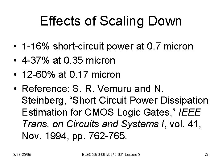
Effects of Scaling Down • • 1 -16% short-circuit power at 0. 7 micron 4 -37% at 0. 35 micron 12 -60% at 0. 17 micron Reference: S. R. Vemuru and N. Steinberg, “Short Circuit Power Dissipation Estimation for CMOS Logic Gates, ” IEEE Trans. on Circuits and Systems I, vol. 41, Nov. 1994, pp. 762 -765. 8/23 -25/05 ELEC 5970 -001/6970 -001 Lecture 2 27

Summary: Short-Circuit Power • Short-circuit power is consumed by each transition (increases with input transition time). • Reduction requires that gate output transition should not be faster than the input transition (faster gates can consume more short-circuit power). • Increasing the output load capacitance reduces short-circuit power. • Scaling down of supply voltage with respect to threshold voltages reduces short-circuit power. 8/23 -25/05 ELEC 5970 -001/6970 -001 Lecture 2 28

Components of Power • Dynamic – Signal transitions • Logic activity • Glitches – Short-circuit • Static – Leakage 8/23 -25/05 ELEC 5970 -001/6970 -001 Lecture 2 29

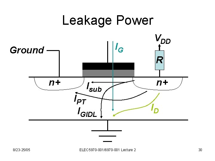
Leakage Power IG Ground R n+ Isub IPT IGIDL 8/23 -25/05 VDD ELEC 5970 -001/6970 -001 Lecture 2 n+ ID 30

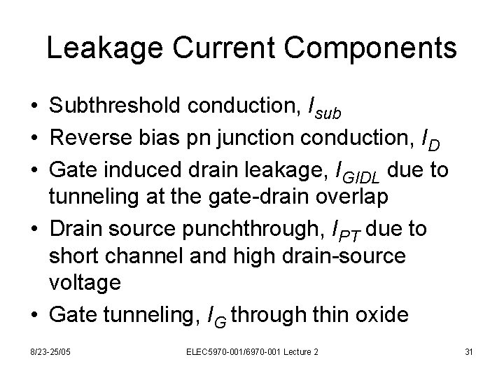
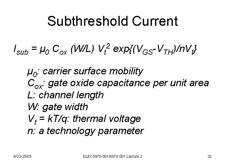
Leakage Current Components • Subthreshold conduction, Isub • Reverse bias pn junction conduction, ID • Gate induced drain leakage, IGIDL due to tunneling at the gate-drain overlap • Drain source punchthrough, IPT due to short channel and high drain-source voltage • Gate tunneling, IG through thin oxide 8/23 -25/05 ELEC 5970 -001/6970 -001 Lecture 2 31

Subthreshold Current Isub = μ 0 Cox (W/L) Vt 2 exp{(VGS-VTH)/n. Vt} μ 0: carrier surface mobility Cox: gate oxide capacitance per unit area L: channel length W: gate width Vt = k. T/q: thermal voltage n: a technology parameter 8/23 -25/05 ELEC 5970 -001/6970 -001 Lecture 2 32

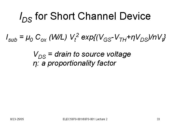
IDS for Short Channel Device Isub = μ 0 Cox (W/L) Vt 2 exp{(VGS-VTH+ηVDS)/n. Vt} VDS = drain to source voltage η: a proportionality factor 8/23 -25/05 ELEC 5970 -001/6970 -001 Lecture 2 33

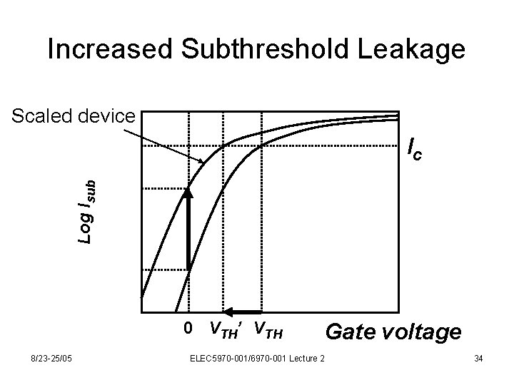
Increased Subthreshold Leakage Scaled device Log Isub Ic 0 VTH’ VTH 8/23 -25/05 Gate voltage ELEC 5970 -001/6970 -001 Lecture 2 34

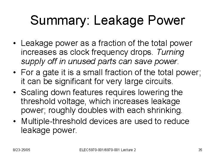
Summary: Leakage Power • Leakage power as a fraction of the total power increases as clock frequency drops. Turning supply off in unused parts can save power. • For a gate it is a small fraction of the total power; it can be significant for very large circuits. • Scaling down features requires lowering the threshold voltage, which increases leakage power; roughly doubles with each shrinking. • Multiple-threshold devices are used to reduce leakage power. 8/23 -25/05 ELEC 5970 -001/6970 -001 Lecture 2 35