ELEC 5970 0016970 001Fall 2005 Special Topics in
- Slides: 31

ELEC 5970 -001/6970 -001(Fall 2005) Special Topics in Electrical Engineering Low-Power Design of Electronic Circuits Dynamic Power Vishwani D. Agrawal James J. Danaher Professor Department of Electrical and Computer Engineering Auburn University, Auburn, AL 36849 http: //www. eng. auburn. edu/~vagrawal@eng. auburn. edu Fall 06, Sep 19, 21 ELEC 5270 -001/6270 -001 Lecture 6 1

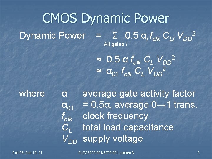
CMOS Dynamic Power = Σ 0. 5 αi fclk CLi VDD 2 All gates i ≈ 0. 5 α fclk CL VDD 2 ≈ α 01 fclk CL VDD 2 where Fall 06, Sep 19, 21 α α 01 fclk CL VDD average gate activity factor = 0. 5α, average 0→ 1 trans. clock frequency total load capacitance supply voltage ELEC 5270 -001/6270 -001 Lecture 6 2

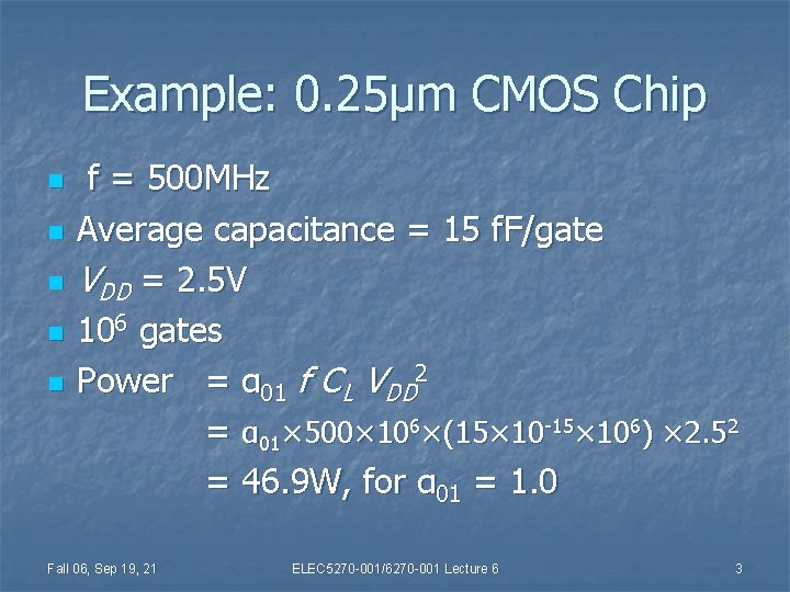
Example: 0. 25μm CMOS Chip n n n f = 500 MHz Average capacitance = 15 f. F/gate VDD = 2. 5 V 106 gates Power = α 01 f CL VDD 2 = α 01× 500× 106×(15× 10 -15× 106) × 2. 52 = 46. 9 W, for α 01 = 1. 0 Fall 06, Sep 19, 21 ELEC 5270 -001/6270 -001 Lecture 6 3

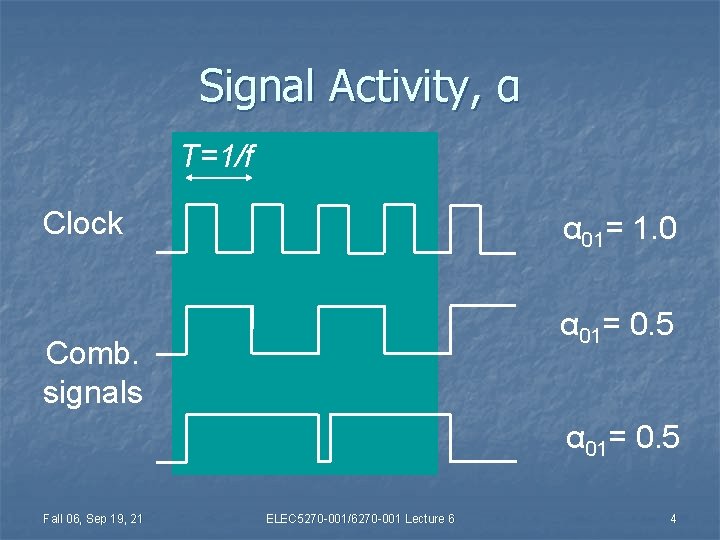
Signal Activity, α T=1/f Clock α 01= 1. 0 α 01= 0. 5 Comb. signals α 01= 0. 5 Fall 06, Sep 19, 21 ELEC 5270 -001/6270 -001 Lecture 6 4

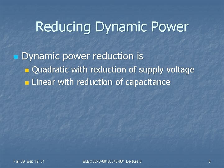
Reducing Dynamic Power n Dynamic power reduction is Quadratic with reduction of supply voltage n Linear with reduction of capacitance n Fall 06, Sep 19, 21 ELEC 5270 -001/6270 -001 Lecture 6 5

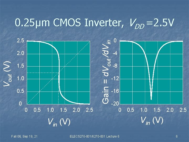
0. 25μm CMOS Inverter, VDD =2. 5 V Gain = d. Vout /d. Vin 2. 5 Vout (V) 2. 0 1. 5 1. 0 0 -4 -8 -12 0. 5 -16 0 0 0. 5 1. 0 1. 5 2. 0 2. 5 -20 0 Vin (V) Fall 06, Sep 19, 21 ELEC 5270 -001/6270 -001 Lecture 6 0. 5 1. 0 1. 5 2. 0 2. 5 Vin (V) 6

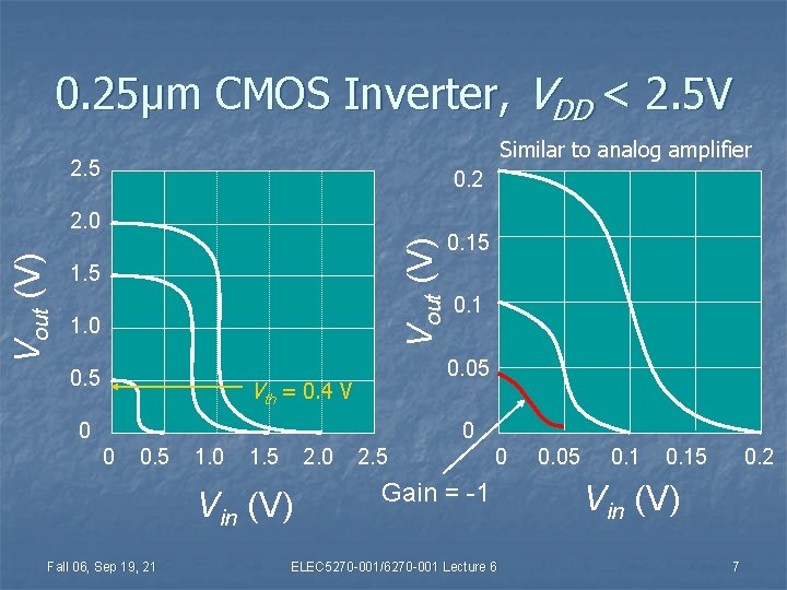
0. 25μm CMOS Inverter, VDD < 2. 5 V Similar to analog amplifier 2. 5 0. 2 Vout (V) 2. 0 1. 5 1. 0 0. 5 0. 1 0. 05 Vth = 0. 4 V 0 0. 5 1. 0 1. 5 2. 0 Vin (V) Fall 06, Sep 19, 21 2. 5 0 Gain = -1 ELEC 5270 -001/6270 -001 Lecture 6 0. 05 0. 15 0. 2 Vin (V) 7

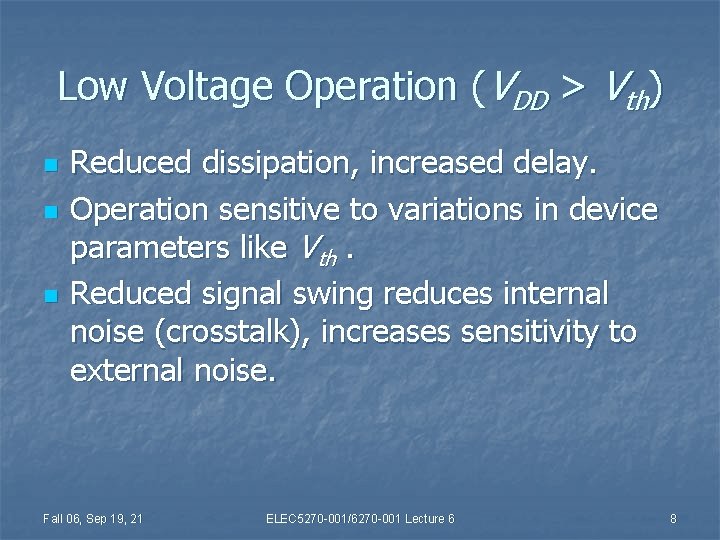
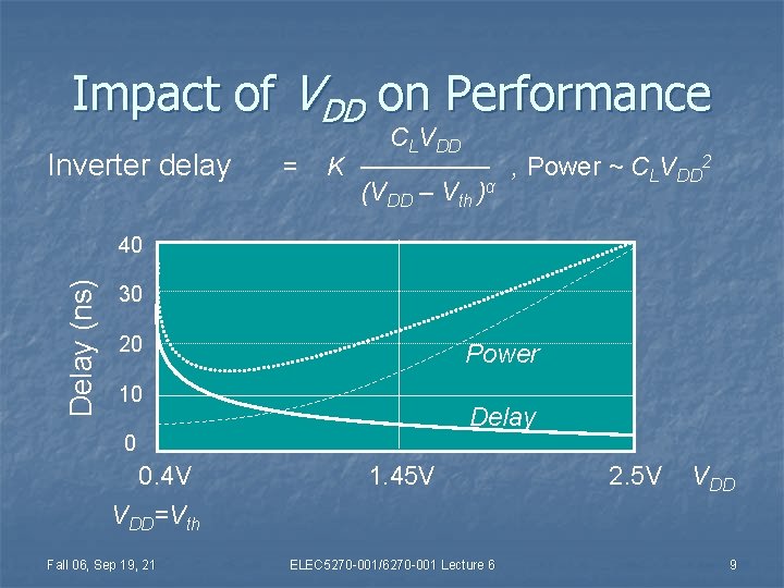
Low Voltage Operation (VDD > Vth) n n n Reduced dissipation, increased delay. Operation sensitive to variations in device parameters like Vth. Reduced signal swing reduces internal noise (crosstalk), increases sensitivity to external noise. Fall 06, Sep 19, 21 ELEC 5270 -001/6270 -001 Lecture 6 8

Impact of VDD on Performance Inverter delay = CLVDD K ─────── , Power ~ CLVDD 2 (VDD – Vth )α Delay (ns) 40 30 20 Power 10 Delay 0 0. 4 V VDD=Vth Fall 06, Sep 19, 21 1. 45 V ELEC 5270 -001/6270 -001 Lecture 6 2. 5 V VDD 9

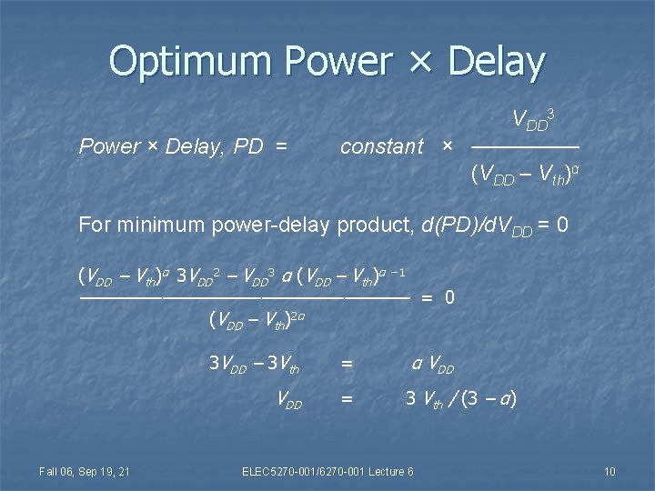
Optimum Power × Delay, PD = VDD 3 constant × ─────── (VDD – Vth)α For minimum power-delay product, d(PD)/d. VDD = 0 (VDD – Vth)α 3 VDD 2 – VDD 3 α (VDD – Vth)α – 1 —————————— = 0 (VDD – Vth)2α Fall 06, Sep 19, 21 3 VDD – 3 Vth = VDD = α VDD 3 Vth / (3 – α) ELEC 5270 -001/6270 -001 Lecture 6 10

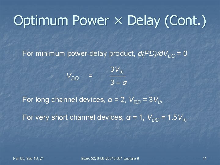
Optimum Power × Delay (Cont. ) For minimum power-delay product, d(PD)/d. VDD = 0 VDD = 3 Vth ─── 3–α For long channel devices, α = 2, VDD = 3 Vth For very short channel devices, α = 1, VDD = 1. 5 Vth Fall 06, Sep 19, 21 ELEC 5270 -001/6270 -001 Lecture 6 11

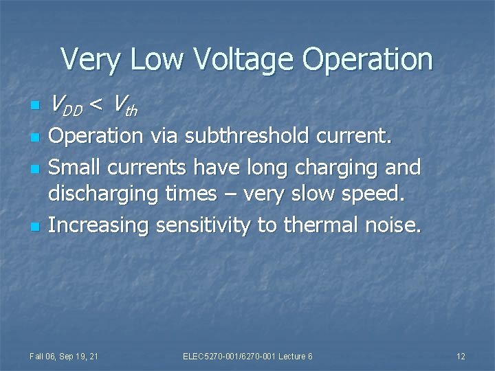
Very Low Voltage Operation n n VDD < Vth Operation via subthreshold current. Small currents have long charging and discharging times – very slow speed. Increasing sensitivity to thermal noise. Fall 06, Sep 19, 21 ELEC 5270 -001/6270 -001 Lecture 6 12

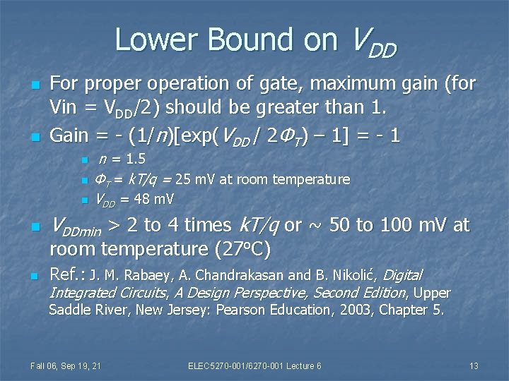
Lower Bound on VDD n n For properation of gate, maximum gain (for Vin = VDD/2) should be greater than 1. Gain = - (1/n)[exp(VDD / 2ΦT) – 1] = - 1 n n n = 1. 5 ΦT = k. T/q = 25 m. V at room temperature VDD = 48 m. V VDDmin > 2 to 4 times k. T/q or ~ 50 to 100 m. V at room temperature (27 o. C) n Ref. : J. M. Rabaey, A. Chandrakasan and B. Nikolić, Digital Integrated Circuits, A Design Perspective, Second Edition, Upper Saddle River, New Jersey: Pearson Education, 2003, Chapter 5. Fall 06, Sep 19, 21 ELEC 5270 -001/6270 -001 Lecture 6 13

Capacitance Reduction n Transistor sizing for Performance n Power n Fall 06, Sep 19, 21 ELEC 5270 -001/6270 -001 Lecture 6 14

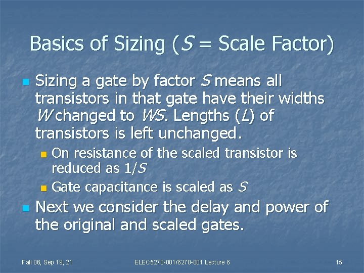
Basics of Sizing (S = Scale Factor) n Sizing a gate by factor S means all transistors in that gate have their widths W changed to WS. Lengths (L) of transistors is left unchanged. On resistance of the scaled transistor is reduced as 1/S n Gate capacitance is scaled as S n n Next we consider the delay and power of the original and scaled gates. Fall 06, Sep 19, 21 ELEC 5270 -001/6270 -001 Lecture 6 15

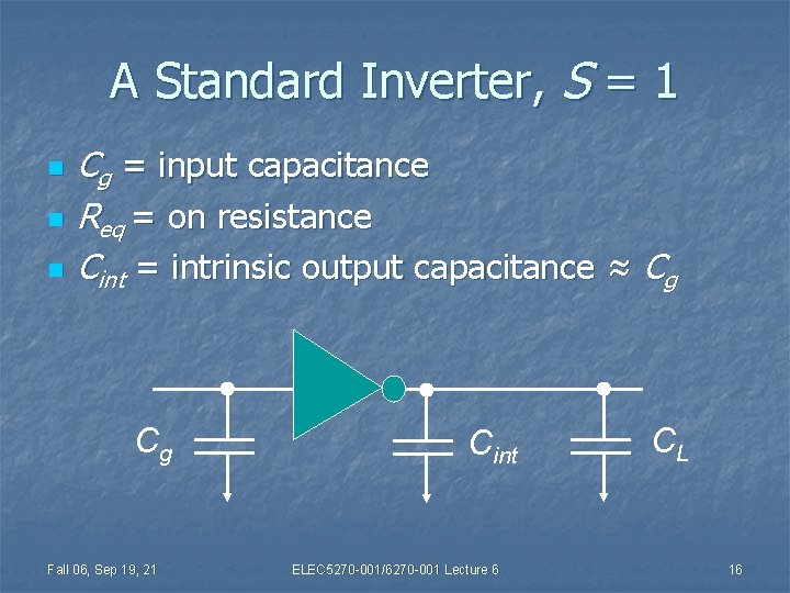
A Standard Inverter, S = 1 n n n Cg = input capacitance Req = on resistance Cint = intrinsic output capacitance ≈ Cg Cg Fall 06, Sep 19, 21 Cint ELEC 5270 -001/6270 -001 Lecture 6 CL 16

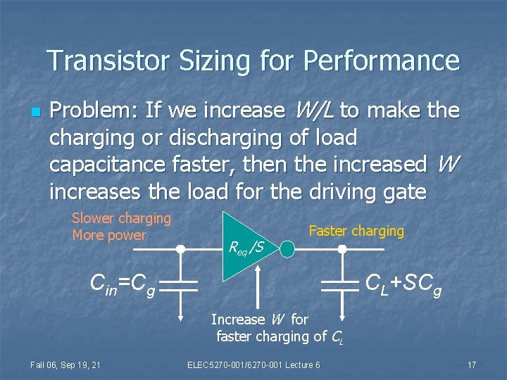
Transistor Sizing for Performance n Problem: If we increase W/L to make the charging or discharging of load capacitance faster, then the increased W increases the load for the driving gate Slower charging More power Req /S Faster charging CL+SCg Cin=Cg Increase W for faster charging of CL Fall 06, Sep 19, 21 ELEC 5270 -001/6270 -001 Lecture 6 17

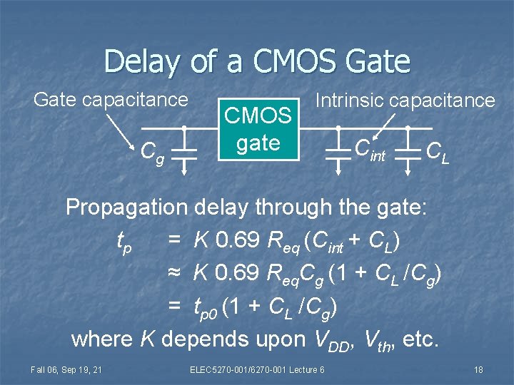
Delay of a CMOS Gate capacitance Cg CMOS gate Intrinsic capacitance Cint CL Propagation delay through the gate: tp = K 0. 69 Req (Cint + CL) ≈ K 0. 69 Req. Cg (1 + CL /Cg) = tp 0 (1 + CL /Cg) where K depends upon VDD, Vth, etc. Fall 06, Sep 19, 21 ELEC 5270 -001/6270 -001 Lecture 6 18

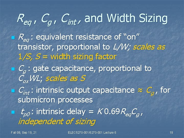
Req , Cg , Cint , and Width Sizing n n Req : equivalent resistance of “on” transistor, proportional to L/W; scales as 1/S, S = width sizing factor Cg : gate capacitance, proportional to Cox. WL; scales as S Cint : intrinsic output capacitance ≈ Cg , for submicron processes tp 0 : intrinsic delay = K 0. 69 Req. Cg , independent of sizing Fall 06, Sep 19, 21 ELEC 5270 -001/6270 -001 Lecture 6 19

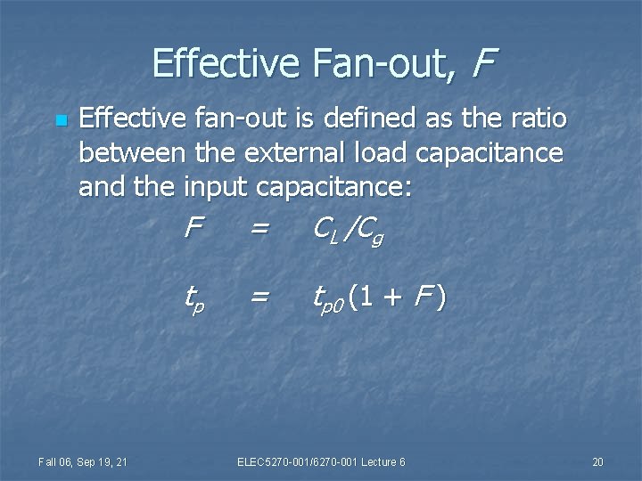
Effective Fan-out, F n Effective fan-out is defined as the ratio between the external load capacitance and the input capacitance: Fall 06, Sep 19, 21 F = CL /Cg tp = tp 0 (1 + F ) ELEC 5270 -001/6270 -001 Lecture 6 20

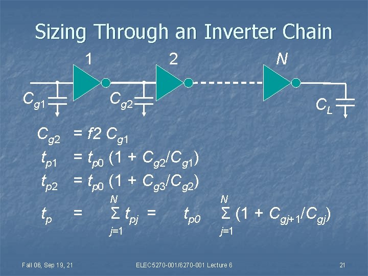
Sizing Through an Inverter Chain 1 Cg 1 2 N Cg 2 CL Cg 2 = f 2 Cg 1 tp 1 = tp 0 (1 + Cg 2/Cg 1) tp 2 = tp 0 (1 + Cg 3/Cg 2) tp = N Σ tpj = j=1 Fall 06, Sep 19, 21 tp 0 N Σ (1 + Cgj+1/Cgj) j=1 ELEC 5270 -001/6270 -001 Lecture 6 21

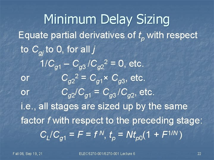
Minimum Delay Sizing Equate partial derivatives of tp with respect to Cgj to 0, for all j 1/Cg 1 – Cg 3 /Cg 22 = 0, etc. or Cg 22 = Cg 1× Cg 3, etc. or Cg 2/Cg 1 = Cg 3 /Cg 2, etc. i. e. , all stages are sized up by the same factor f with respect to the preceding stage: CL/Cg 1 = F = f N, tp = Ntp 0(1 + F 1/N ) Fall 06, Sep 19, 21 ELEC 5270 -001/6270 -001 Lecture 6 22

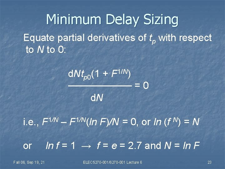
Minimum Delay Sizing Equate partial derivatives of tp with respect to N to 0: d. Ntp 0(1 + F 1/N) ───── = 0 d. N i. e. , F 1/N – F 1/N(ln F)/N = 0, or ln (f N) = N or Fall 06, Sep 19, 21 ln f = 1 → f = e = 2. 7 and N = ln F ELEC 5270 -001/6270 -001 Lecture 6 23

Further Reading B. S. Cherkauer and E. G. Friedman, “A Unified Design Methodology for CMOS Tapered Buffers, ” IEEE Trans. VLSI Systems, vol. 3, no. 1, pp. 99 -111, March 1995. Fall 06, Sep 19, 21 ELEC 5270 -001/6270 -001 Lecture 6 24

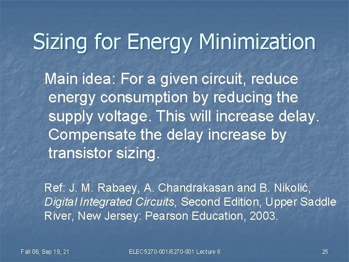
Sizing for Energy Minimization Main idea: For a given circuit, reduce energy consumption by reducing the supply voltage. This will increase delay. Compensate the delay increase by transistor sizing. Ref: J. M. Rabaey, A. Chandrakasan and B. Nikolić, Digital Integrated Circuits, Second Edition, Upper Saddle River, New Jersey: Pearson Education, 2003. Fall 06, Sep 19, 21 ELEC 5270 -001/6270 -001 Lecture 6 25

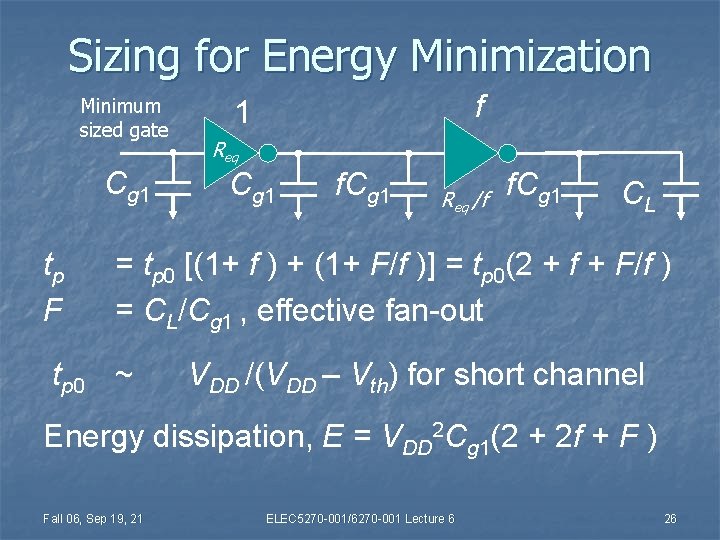
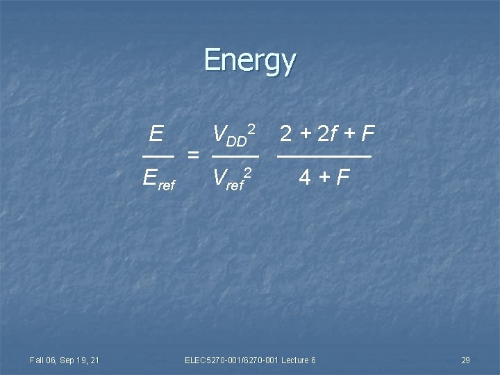
Sizing for Energy Minimization Minimum sized gate Cg 1 tp F f 1 Req Cg 1 f. Cg 1 Req /f f. Cg 1 CL = tp 0 [(1+ f ) + (1+ F/f )] = tp 0(2 + f + F/f ) = CL/Cg 1 , effective fan-out tp 0 ~ VDD /(VDD – Vth) for short channel Energy dissipation, E = VDD 2 Cg 1(2 + 2 f + F ) Fall 06, Sep 19, 21 ELEC 5270 -001/6270 -001 Lecture 6 26

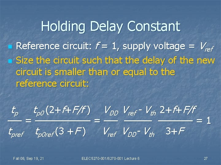
Holding Delay Constant n n Reference circuit: f = 1, supply voltage = Vref Size the circuit such that the delay of the new circuit is smaller than or equal to the reference circuit: tp tp 0 (2+f+F/f ) VDD Vref - Vth 2+f+F/f ── = ──── = ── ───── = 1 tpref tp 0 ref (3 +F ) Vref VDD- Vth 3+F Fall 06, Sep 19, 21 ELEC 5270 -001/6270 -001 Lecture 6 27

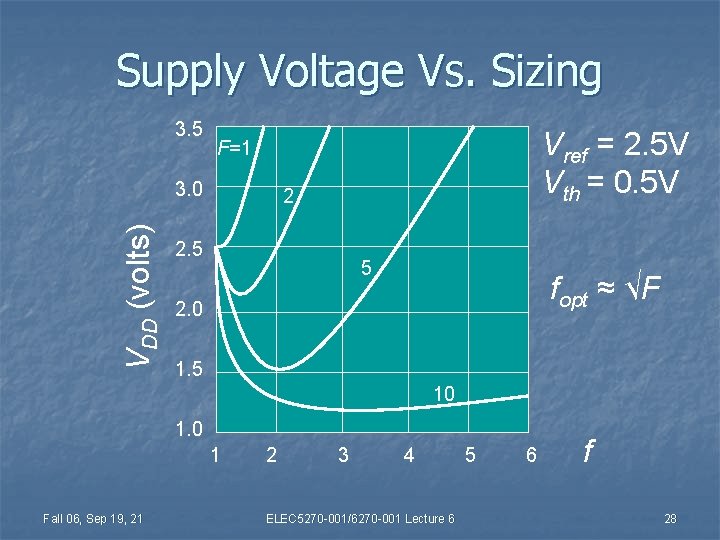
Supply Voltage Vs. Sizing 3. 5 3. 0 VDD (volts) Vref = 2. 5 V Vth = 0. 5 V F=1 2 2. 5 5 fopt ≈ √F 2. 0 1. 5 10 1. 0 1 Fall 06, Sep 19, 21 2 3 4 ELEC 5270 -001/6270 -001 Lecture 6 5 6 f 28

Energy E VDD 2 2 + 2 f + F ── = ────── Eref Vref 2 4+F Fall 06, Sep 19, 21 ELEC 5270 -001/6270 -001 Lecture 6 29

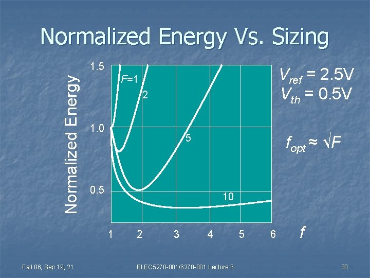
Normalized Energy Vs. Sizing Normalized Energy 1. 5 2 1. 0 5 fopt ≈ √F 0. 5 10 1 Fall 06, Sep 19, 21 Vref = 2. 5 V Vth = 0. 5 V F=1 2 3 4 ELEC 5270 -001/6270 -001 Lecture 6 5 6 f 30

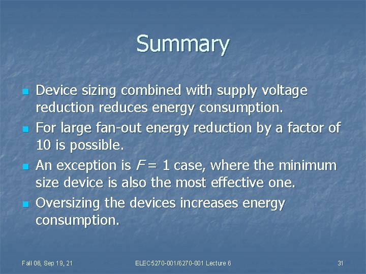
Summary n n Device sizing combined with supply voltage reduction reduces energy consumption. For large fan-out energy reduction by a factor of 10 is possible. An exception is F = 1 case, where the minimum size device is also the most effective one. Oversizing the devices increases energy consumption. Fall 06, Sep 19, 21 ELEC 5270 -001/6270 -001 Lecture 6 31