ELEC 5970 0016970 001Fall 2005 Special Topics in
- Slides: 18

ELEC 5970 -001/6970 -001(Fall 2005) Special Topics in Electrical Engineering Low-Power Design of Electronic Circuits Pseudo-n. MOS, Dynamic CMOS and Domino CMOS Logic Vishwani D. Agrawal James J. Danaher Professor Department of Electrical and Computer Engineering Auburn University http: //www. eng. auburn. edu/~vagrawal@eng. auburn. edu 10/25/05 ELEC 5970 -001/6970 -001 Lecture 15 1

Why Not Static CMOS? • Advantages: Static (robust) operation, low power, scalable with technology. • Disadvantages: – Large size: An N input gate requires 2 N transistors. – Large capacitance: Each fanout must drive two devices. • Alternatives: Pass-transistor logic (PTL), pseudon. MOS, dynamic CMOS, domino CMOS. 10/25/05 ELEC 5970 -001/6970 -001 Lecture 15 2

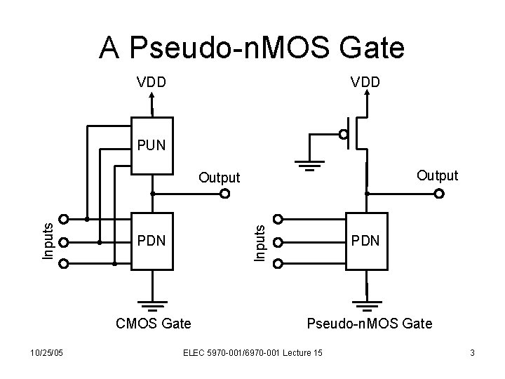
A Pseudo-n. MOS Gate VDD PUN Output Inputs Output PDN CMOS Gate 10/25/05 PDN Pseudo-n. MOS Gate ELEC 5970 -001/6970 -001 Lecture 15 3

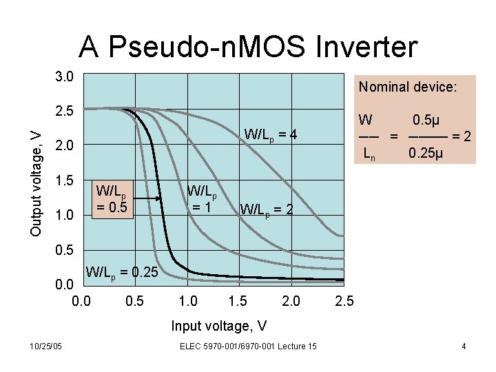
A Pseudo-n. MOS Inverter 3. 0 Nominal device: Output voltage, V 2. 5 W 0. 5μ ── = ──── = 2 Ln 0. 25μ W/Lp = 4 2. 0 1. 5 W/Lp = 0. 5 1. 0 W/Lp =1 W/Lp = 2 0. 5 W/Lp = 0. 25 0. 0 0. 5 1. 0 1. 5 2. 0 2. 5 Input voltage, V 10/25/05 ELEC 5970 -001/6970 -001 Lecture 15 4

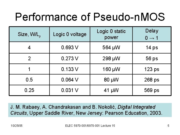
Performance of Pseudo-n. MOS Delay 0→ 1 Size, W/Lp Logic 0 voltage Logic 0 static power 4 0. 693 V 564 μW 14 ps 2 0. 273 V 298 μW 56 ps 1 0. 133 V 160 μW 123 ps 0. 5 0. 064 V 80 μW 268 ps 0. 25 0. 031 V 41 μW 569 ps J. M. Rabaey, A. Chandrakasan and B. Nokolić, Digital Integrated Circuits, Upper Saddle River, New Jersey: Pearson Education, 2003. 10/25/05 ELEC 5970 -001/6970 -001 Lecture 15 5

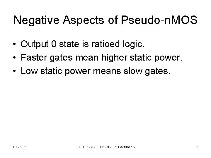
Negative Aspects of Pseudo-n. MOS • Output 0 state is ratioed logic. • Faster gates mean higher static power. • Low static power means slow gates. 10/25/05 ELEC 5970 -001/6970 -001 Lecture 15 6

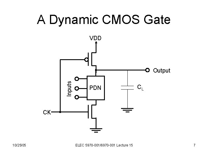
A Dynamic CMOS Gate VDD Inputs Output PDN CL CK 10/25/05 ELEC 5970 -001/6970 -001 Lecture 15 7

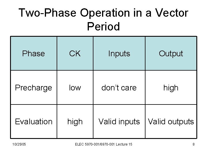
Two-Phase Operation in a Vector Period Phase CK Inputs Output Precharge low don’t care high Evaluation high 10/25/05 Valid inputs Valid outputs ELEC 5970 -001/6970 -001 Lecture 15 8

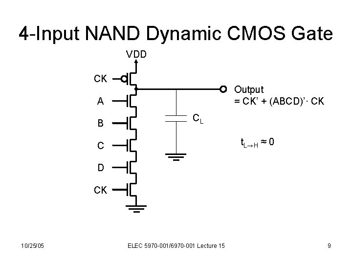
4 -Input NAND Dynamic CMOS Gate VDD CK Output = CK’ + (ABCD)’∙ CK A B CL t. L→H ≈ 0 C D CK 10/25/05 ELEC 5970 -001/6970 -001 Lecture 15 9

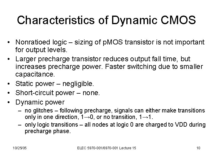
Characteristics of Dynamic CMOS • Nonratioed logic – sizing of p. MOS transistor is not important for output levels. • Larger precharge transistor reduces output fall time, but increases precharge power. Faster switching due to smaller capacitance. • Static power – negligible. • Short-circuit power – none. • Dynamic power – no glitches – following precharge, signals can either make transitions only in one direction, 1→ 0, or no transition, 1→ 1. – only logic transitions – all nodes at logic 0 are charged to VDD during precharge phase. 10/25/05 ELEC 5970 -001/6970 -001 Lecture 15 10

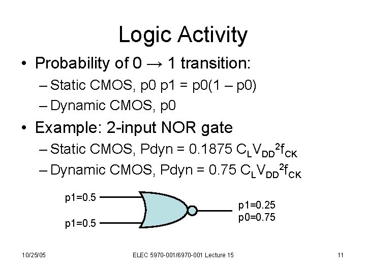
Logic Activity • Probability of 0 → 1 transition: – Static CMOS, p 0 p 1 = p 0(1 – p 0) – Dynamic CMOS, p 0 • Example: 2 -input NOR gate – Static CMOS, Pdyn = 0. 1875 CLVDD 2 f. CK – Dynamic CMOS, Pdyn = 0. 75 CLVDD 2 f. CK p 1=0. 5 p 1=0. 25 p 0=0. 75 p 1=0. 5 10/25/05 ELEC 5970 -001/6970 -001 Lecture 15 11

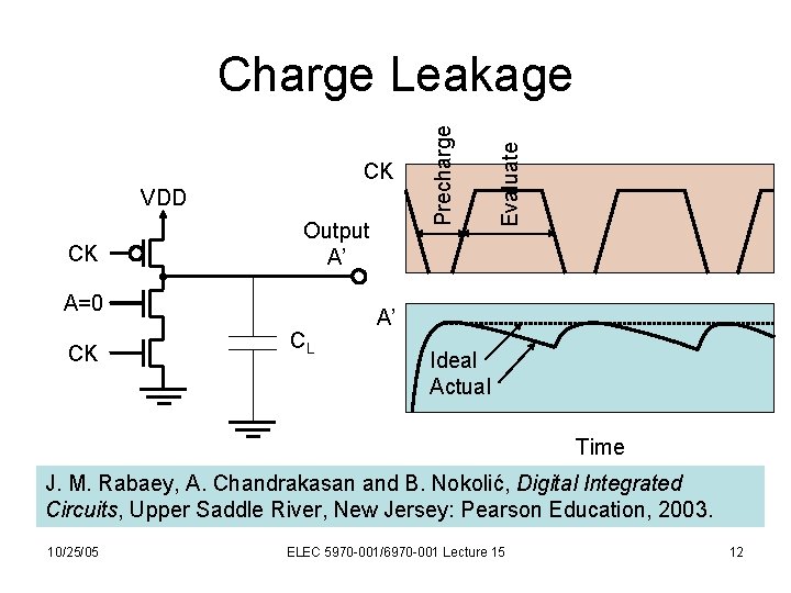
VDD CK Output A’ A=0 CK CL Evaluate CK Precharge Charge Leakage A’ Ideal Actual Time J. M. Rabaey, A. Chandrakasan and B. Nokolić, Digital Integrated Circuits, Upper Saddle River, New Jersey: Pearson Education, 2003. 10/25/05 ELEC 5970 -001/6970 -001 Lecture 15 12

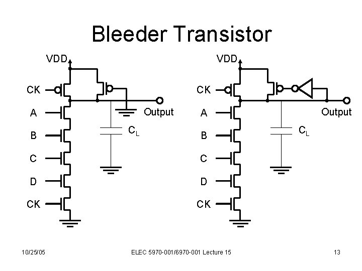
Bleeder Transistor VDD CK CK Output A B CL B C C D D CK CK 10/25/05 Output A ELEC 5970 -001/6970 -001 Lecture 15 CL 13

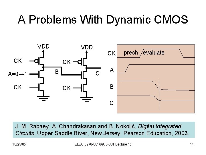
A Problems With Dynamic CMOS VDD CK A=0→ 1 CK CK prech. evaluate CK B C CK A B C J. M. Rabaey, A. Chandrakasan and B. Nokolić, Digital Integrated Circuits, Upper Saddle River, New Jersey: Pearson Education, 2003. 10/25/05 ELEC 5970 -001/6970 -001 Lecture 15 14

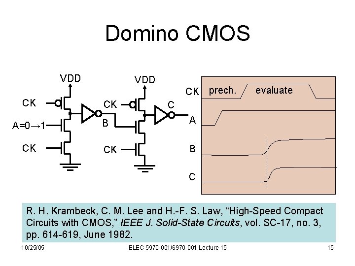
Domino CMOS VDD CK A=0→ 1 CK VDD CK CK prech. evaluate C B A CK B C R. H. Krambeck, C. M. Lee and H. -F. S. Law, “High-Speed Compact Circuits with CMOS, ” IEEE J. Solid-State Circuits, vol. SC-17, no. 3, pp. 614 -619, June 1982. 10/25/05 ELEC 5970 -001/6970 -001 Lecture 15 15

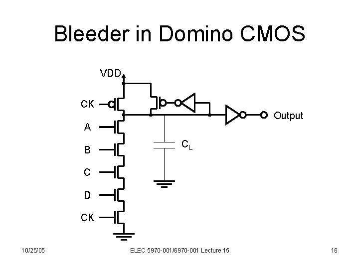
Bleeder in Domino CMOS VDD CK Output A B CL C D CK 10/25/05 ELEC 5970 -001/6970 -001 Lecture 15 16

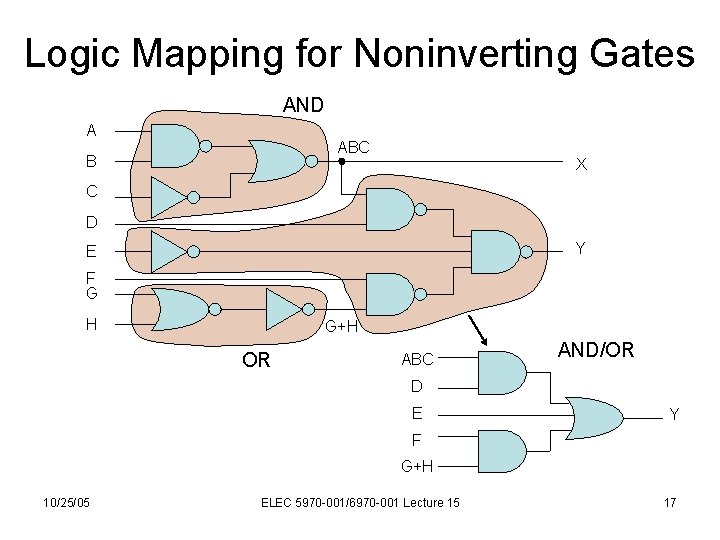
Logic Mapping for Noninverting Gates AND A ABC B X C D Y E F G H G+H OR ABC AND/OR D E Y F G+H 10/25/05 ELEC 5970 -001/6970 -001 Lecture 15 17

Selecting a Logic Style • Static CMOS: most reliable and predictable, reasonable in power and speed, voltage scaling and device sizing are well understood. • Pass-transistor logic: beneficial for multiplexer and XOR dominated circuits like adders, etc. • For large fanin gates, static CMOS is inefficient; a choice can be made between pseudo-n. MOS, dynamic CMOS and domino CMOS. 10/25/05 ELEC 5970 -001/6970 -001 Lecture 15 18